

LTC3220/LTC3220-1
360mA Universal
18-Channel LED Driver
FEATURES
n
Eighteen 20mA Universal Current Sources with
64-Step Linear Brightness Control
n
Independent On/Off, Brightness Level, Blinking and
Gradation Control for Each Current Source Using
2
2-Wire I
n
Low Noise Multi-Mode Charge Pump (1x, 1.5x, 2x)
C Interface
Provides Up to 91% Effi ciency
n
Slew Limited Switching Reduces Conducted and
Radiated Noise (EMI)
n
Up to 360mA Total Output Current
n
Internal Current Reference
n
Single Reset Pin for Asynchronous Shutdown and
Reset of All Data Registers
n
Two I2C Addresses Are Available (LTC3220: 0011100,
LTC3220-1: 0011101)
n
Automatic or Forced Mode Switching
n
Internal Soft-Start Limits Inrush Current
n
Short-Circuit/Thermal Protection
n
4mm × 4mm Ultrathin (0.55mm) 28-Lead QFN
Package
APPLICATIONS
n
Video Phones with QVGA+ Displays
n
Keypad Lighting
n
General/Miscellaneous Lighting
DESCRIPTION
The LTC3220/LTC3220-1 are highly integrated multi-display
LED drivers. These parts contain a high effi ciency, low noise
charge pump to provide power to up to eighteen universal
LED current sources. The LTC3220/LTC3220-1 require
only fi ve small ceramic capacitors to form a complete
LED power supply and current controller.
The LED currents are set by an internal precision current reference. Independent dimming, on/off, blinking
and gradation control for all universal current sources
is achieved via the I
are available to adjust brightness levels independently for
each universal LED current source.
The LTC3220/LTC3220-1 charge pump optimizes effi ciency
based on the voltage across the LED current sources. The
part powers up in 1x mode and will automatically switch
to boost mode whenever any enabled LED current source
begins to enter dropout. The fi rst dropout switches the
parts into 1.5x mode and a subsequent dropout switches
the LTC3220/LTC3220-1 into 2x mode. The parts reset to
1x mode whenever a data bit is updated via the I
L, LT, LTC and LTM are registered trademarks of Linear Technology Corporation.
All other trademarks are the property of their respective owners.
Protected by U.S. Patents including 6411531.
2
C serial interface. 6-bit linear DACs
2
C port.
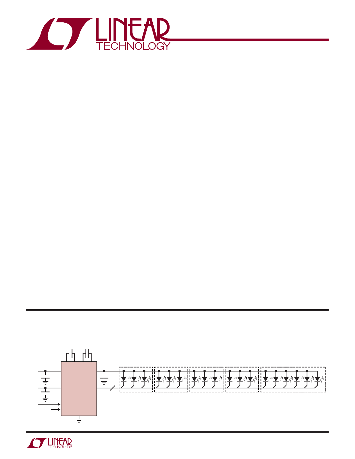
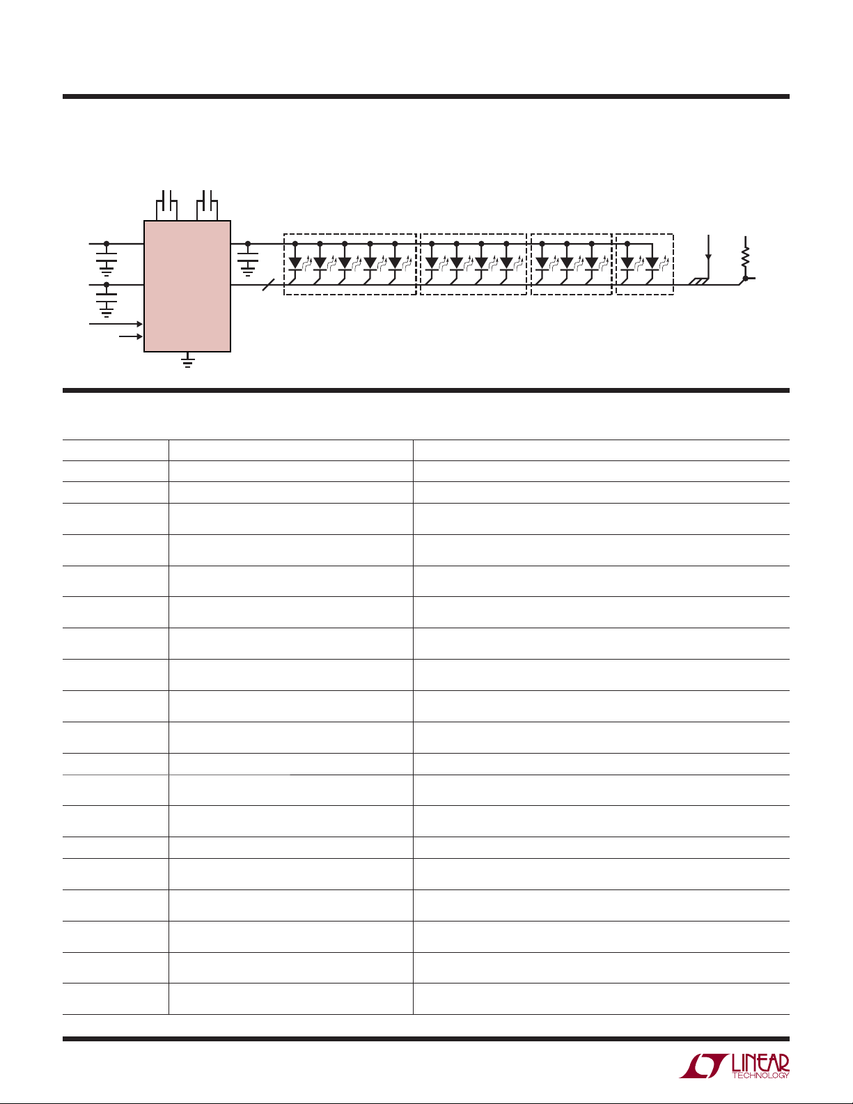
TYPICAL APPLICATION
C2
2.2μFC32.2μF
C1P
C1M
C2P
V
IN
DV
CC
I2C
RESET
C1
2.2μF
0.1μF
V
IN
LTC3220-1
DV
CC
SCL/SDA
RST
LTC3220
ULED1-18
GND
C2M
CPO
C4
4.7μF
18
RGB1
6-LED Main, 4 RGB LEDs
RGB2 RGB3 RGB4 MAIN
3220 TA01
32201fb
1
LTC3220/LTC3220-1
(Notes 1, 4)
VIN, DVCC, CPO to GND ................................ –0.3V to 6V
ULED1-ULED18 to GND ............................... –0.3V to 6V
SDA, SCL, RST............................–0.3V to (DV
(Continuous) (Note 2) ..................................360mA
I
CPO
I
ULED1-18
(Note 2) ..................................................25mA
CPO Short-Circuit Duration .............................. Indefi nite
Operating Temperature Range (Note 3)
LTC3220E/LTC3220E-1 ........................ –40°C to 85°C
LTC3220I/LTC3220I-1 ........................ –40°C to 125°C
Storage Temperature Range ...................–65°C to 150°C
+ 0.3V)
CC
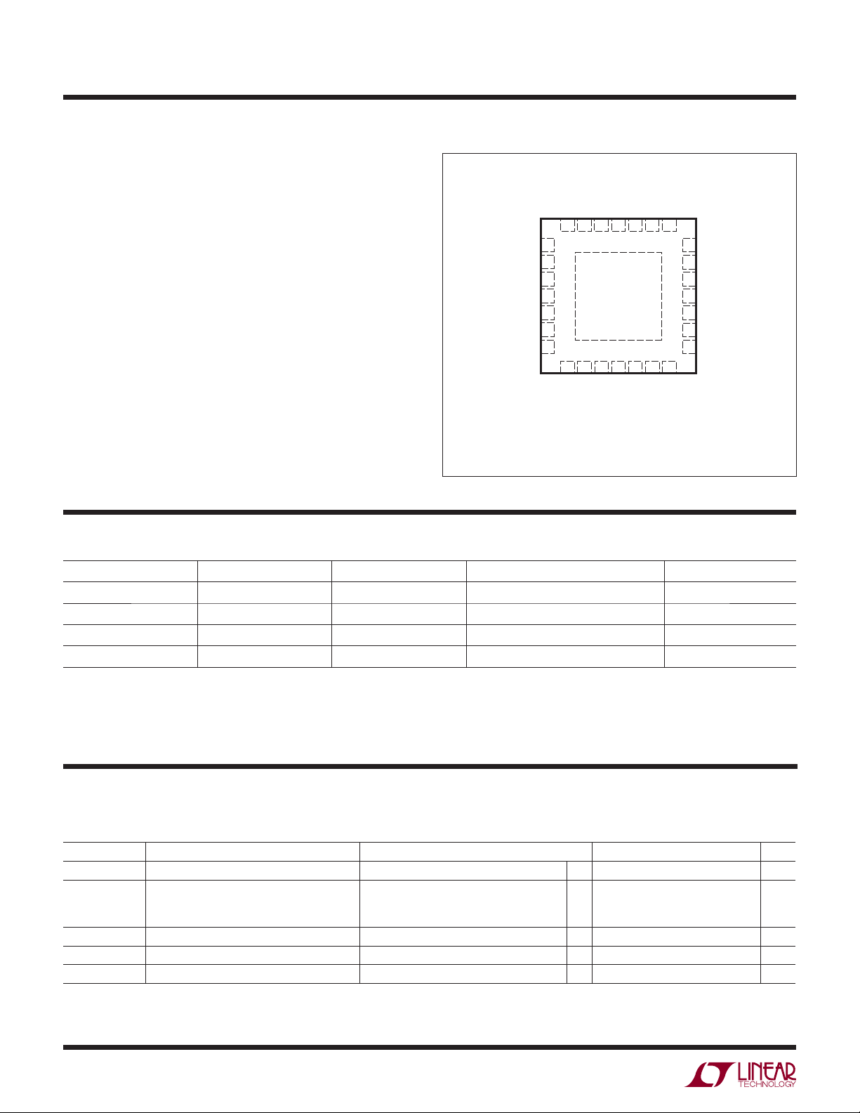
PIN CONFIGURATION ABSOLUTE MAXIMUM RATINGS
TOP VIEW
CPO
C1P
C2P
RST
VINC1M
C2M
28 27 26 25 24 23
1
ULED1
ULED2
2
ULED3
3
ULED4
4
ULED5
5
ULED6
6
ULED7
7
8 9
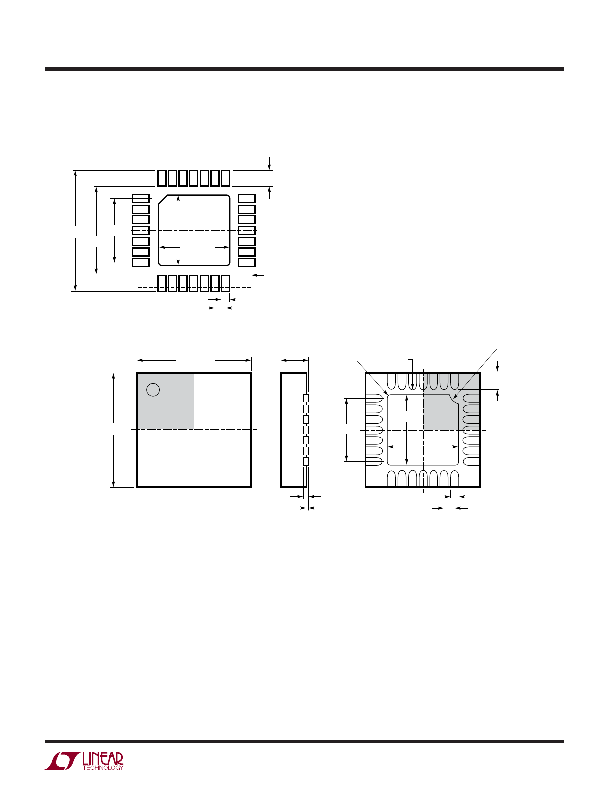
28-LEAD UTQFN (4mm s 4mm)
T
EXPOSED PAD (PIN 29) IS GND, MUST BE SOLDERED TO PCB
JMAX
29
11 12 13 14
10
CC
SCL
DV
ULED8
ULED9
PF PACKAGE
= 125°C, θJA = 37°C/W
SDA
22
ULED10
ULED11
21
20
19
18
17
16
15
ULED18
ULED17
ULED16
ULED15
ULED14
ULED13
ULED12
ORDER INFORMATION
LEAD FREE FINISH TAPE AND REEL PART MARKING* PACKAGE DESCRIPTION TEMPERATURE RANGE
LTC3220EPF#PBF LTC3220EPF#TRPBF 3220T 28-Lead UTQFN (4mm × 4mm) –40°C to 85°C
LTC3220EPF-1#PBF LTC3220EPF-1#TRPBF 2201T 28-Lead UTQFN (4mm × 4mm) –40°C to 85°C
LTC3220IPF#PBF LTC3220IPF#TRPBF 3220T 28-Lead UTQFN (4mm × 4mm) –40°C to 125°C
LTC3220IPF-1#PBF LTC3220IPF-1#TRPBF 2201T 28-Lead UTQFN (4mm × 4mm) –40°C to 125°C
Consult LTC Marketing for parts specifi ed with wider operating temperature ranges. *The temperature grade is identifi ed by a label on the shipping container.
Consult LTC Marketing for information on non-standard lead based fi nish parts.
For more information on lead free part marking, go to: http://www.linear.com/leadfree/
For more information on tape and reel specifi cations, go to: http://www.linear.com/tapeandreel/
ELECTRICAL CHARACTERISTICS
The l denotes the specifi cations which apply over the full operating
temperature range, otherwise specifi cations are at TA = 25°C. VIN = 3.6V, DVCC = 3V, RST = high, C1 = C2 = C3 = 2.2μF, C4 = 4.7μF,
unless otherwise noted.
SYMBOL PARAMETER CONDITIONS MIN TYP MAX UNITS
Operating Voltage
V
IN
Operating Current I
I
VIN
UVLO Threshold 1V
DV
CC
Operating Voltage
DV
CC
UVLO Threshold 1.5 V
V
IN
= 0, 1x Mode
CPO
I
= 0, 1.5x Mode
CPO
I
= 0, 2x Mode
CPO
l
2.9 5.5 V
580
2.4
3.2
l
1.5 5.5 V
μA
mA
mA
2
32201fb
LTC3220/LTC3220-1
ELECTRICAL CHARACTERISTICS
The l denotes the specifi cations which apply over the full operating
temperature range, otherwise specifi cations are at T
unless otherwise noted.
SYMBOL PARAMETER CONDITIONS MIN TYP MAX UNITS
Shutdown Current
V
IN
Shutdown Current
DV
CC
Universal LED Current, 6-Bit Linear DACs, ULED = 1V
Full-Scale LED Current
Minimum (I
Minimum Programmable Current ULED Data Register Programmed to
LED Current Matching Any Two Outputs, 50% of FS 1.5 %
LED Dropout Voltage I
Blink Rate Period REG19, D3 and D4 1.25
ULED Up/Down Gradation Ramp Times REG19, D1 and D2 0.24
Gradation Period REG19, D1 and D2 0.313
General Purpose Output Mode (GPO) I
V
OL
LED Turn-On Delay From Stop Bit, Part Enabled 4 μs
Charge Pump (CPO)
1x Mode Output Impedance 0.6 Ω
1.5x Mode Output Impedance V
2x Mode Output Impedance V
CPO Regulation Voltage 1.5x Mode, I
Clock Frequency
CPO Short-Circuit Detection
Threshold Voltage
Test Current CPO = 0V
SDA, SCL, RST
V
IL
V
IH
I
IH
I
IL
V
OL
Digital Output Low (SDA) I
RST Timing Reset Pulse Duration 10 ns
Serial Port Timing (Notes 6, 7)
f
t
SCL
BUF
Clock Operating Frequency 400 kHz
Bus Free Time Between Stop and Start
Condition
t
HD,STA
t
SU,STA
t
SU,STO
Hold Time After (Repeated) Start Condition 0.6 μs
Repeated Start Condition Setup Time 0.6 μs
Stop Condition Setup Time 0.6 μs
) LED Current Step 0.314 mA
LSB
= 25°C. VIN = 3.6V, DVCC = 3V, RST = high, C1 = C2 = C3 = 2.2μF, C4 = 4.7μF,
A
l
l
l
18 20 22 mA
3.2 7 μA
1μA
0.395 mA
0b00000001
= FS 120 mV
LED
2.5
0.48
0.96
0.410
0.625
1.25
= 1mA, Single Output Enabled 5 mV
OUT
= 3V, V
IN
= 3V, V
IN
2x Mode, I
SDA, SCL, RST = DV
SDA, SCL, RST = 0V
PULLUP
= 4.2V (Note 5) 3.6 Ω
CPO
= 4.8V (Note 5) 4.1 Ω
CPO
CPO
CPO
= 3mA
= 20mA
= 20mA
CC
l
0.65 0.85 1.05 MHz
l
0.4 1.3 V
l
10 30 mA
l
l
0.7 • DV
l
–1 1 μA
l
–1 1 μA
l
4.5
5.03
CC
0.12 0.4 V
0.820
1.640
0.3 • DV
CC
1.3 μs
Sec
Sec
Sec
Sec
Sec
Sec
Sec
Sec
V
V
V
V
32201fb
3
LTC3220/LTC3220-1
ELECTRICAL CHARACTERISTICS
The l denotes the specifi cations which apply over the full operating
temperature range, otherwise specifi cations are at T
unless otherwise noted.
SYMBOL PARAMETER CONDITIONS MIN TYP MAX UNITS
t
HD,DAT(OUT)
t
HD,DAT(IN)
t
SU,DAT
t
LOW
t
HIGH
t
f
t
r
t
SP
Data Hold Time 0 900 ns
Input Data Hold Time 0 ns
Data Setup Time 100 ns
Clock Low Period 1.3 μs
Clock High Period 0.6 μs
Clock Data Fall Time 20 300 ns
Clock Data Rise Time 20 300 ns
Spike Supression Time 50 ns
= 25°C. VIN = 3.6V, DVCC = 3V, RST = high, C1 = C2 = C3 = 2.2μF, C4 = 4.7μF,
A
Note 1: Stresses beyond those listed under Absolute Maximum Ratings
may cause permanent damage to the device. Exposure to any Absolute
Maximum Rating condition for extended periods may affect device
reliability and lifetime.
Note 2: Based on long term current density limitations.
Note 3: The LTC3220E/LTC3220E-1 are guaranteed to meet performance
specifi cations from 0°C to 85°C. Specifi cations over the –40°C to 85°C
operating temperature range are assured by design, characterization and
correlation with statistical process controls. The LTC3220I/LTC3220I-1
Note 4: These devices include overtemperature protection that is intended
to protect the devices during momentary overload conditions. Junction
temperatures will exceed 125°C when overtemperature protection is
active. Continuous operation above the specifi ed maximum operating
junction temperature may result in device degradation or failure.
Note 5: 1.5x mode output impedance is defi ned as (1.5V
2x mode output impedance is defi ned as (2V
Note 6: All values are referenced to V
and VIL levels.
IH
Note 7: Guaranteed by design.
are guaranteed to meet performance specifi cations over the full –40°C to
125°C operating temperature range.
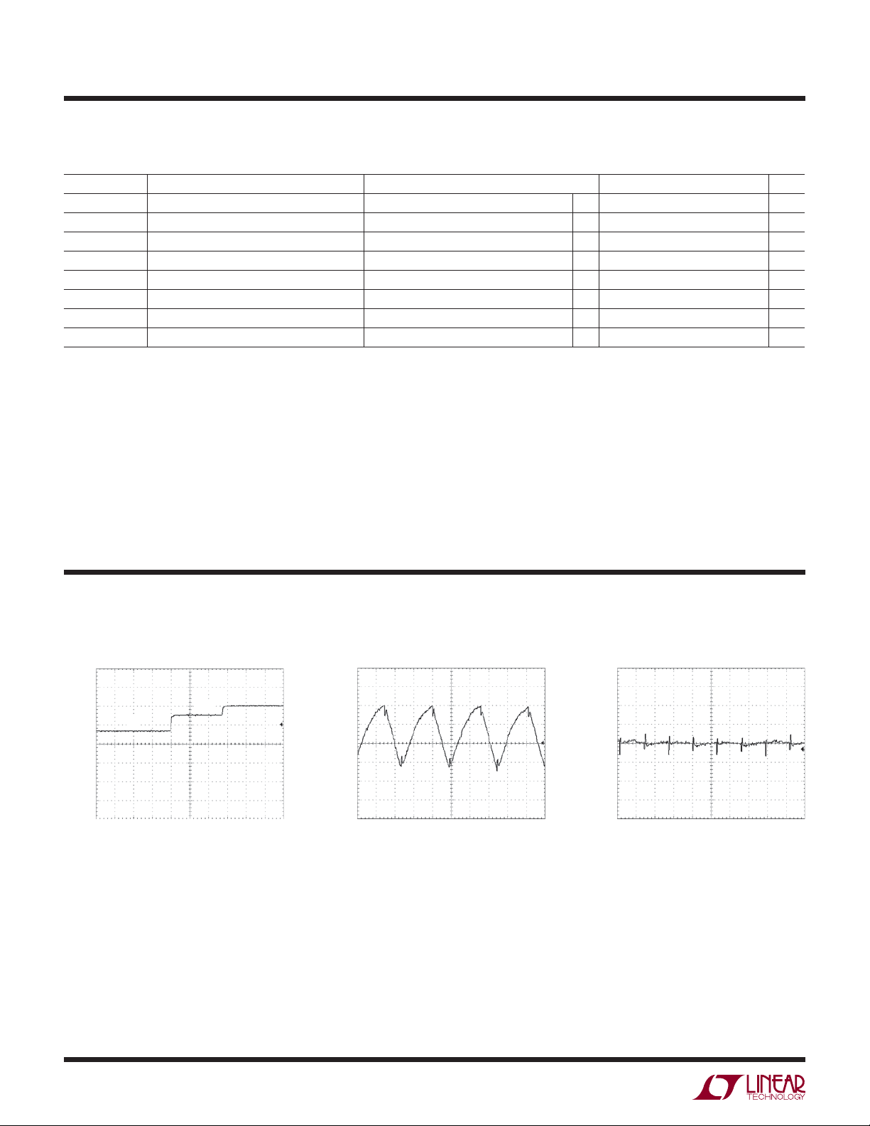
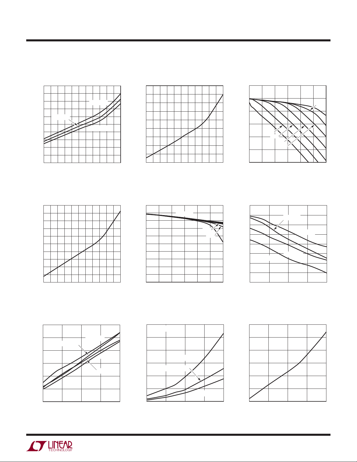
TYPICAL PERFORMANCE CHARACTERISTICS
TA = 25°C unless otherwise noted.
Mode Switch Dropout Times 1.5x Mode CPO Ripple 2x Mode CPO Ripple
2s
V
CPO
20mV/DIV
AC COUPLED
V
CPO
20mV/DIV
AC COUPLED
V
CPO
1V/DIV
1.5s
1s
– V
)/I
CPO
OUT
.
CPO
)/I
IN
OUT
.
– V
IN
4
= 3.6V 250μs/DIV
V
IN
3220 G01
V
I
C
IN
CPO
CPO
= 3.6V
= 200mA
= 4.7μF
500ns/DIV
3220 G02
V
I
C
IN
CPO
CPO
= 3.6V
= 200mA
= 4.7μF
500ns/DIV
3220 G03
32201fb
LTC3220/LTC3220-1
TYPICAL PERFORMANCE CHARACTERISTICS
1x Mode Switch Resistance
vs Temperature
0.80
0.75
0.70
0.65
0.60
0.55
0.50
0.45
SWITCH RESISTANCE (Ω)
0.40
0.35
0.30
VIN = 3.6V
–25 –10 20 35 50 65 80 95 110
–40
5
TEMPERATURE (°C)
VIN = 3.3V
VIN = 3.9V
2x Mode Charge Pump Open-Loop
Output Resistance vs Temperature
4.9
4.7
4.5
4.3
4.1
3.9
3.7
3.5
3.3
OPEN-LOOP OUTPUT RESISTANCE (Ω)
3.1
2.9
–25 –10 35205 50 65 80 110 125
–40
TEMPERATURE (°C)
125
3220 G04
95
3220 G07
1.5x Mode Charge Pump Open-Loop
Output Resistance vs Temperature
4.5
4.3
4.1
3.9
3.5
3.3
3.1
2.9
2.7
OPEN-LOOP OUTPUT RESISTANCE (Ω)
2.5
–40
–25 –10 5 6520 35 50 80 95 110
TEMPERATURE (°C)
2x Mode CPO Voltage vs I
5.2
5.1
5.0
4.9
4.8
4.7
4.6
CPO VOLTAGE (V)
4.5
4.4
4.3
4.2
60
0
120
3.3V-3.6V
180 240
I
(mA)
CPO
TA = 25°C unless otherwise noted.
1.5x Mode CPO Voltage vs I
4.8
4.6
4.4
3220 G05
125
4.2
CPO VOLTAGE (V)
4.0
3.8
3.6
3V
3.1V
0
60
Oscillator Frequency
CPO
3.2V
3.1V
300
3V
360
3220 G08
vs VIN Voltage
810
800
790
780
770
760
FREQUENCY (kHz)
750
740
730
TA = 85°C
2.9
3.55
3.2V
3.3V
3.4V
120 180 240
I
(mA)
CPO
TA = 25°C
TA = –45°C
TA = 125°C
4.2
VIN VOLTAGE (V)
3.6V
300 360
4.85
CPO
3.5V
3220 G06
5.5
3220 G09
VIN Shutdown Current
vs VIN Voltage
7.5
6.5
5.5
4.5
3.5
SHUTDOWN CURRENT (μA)
IN
V
2.5
1.5
2.9
TA = 85°C
3.55 4.2 4.85 5.5
VOLTAGE (V)
TA = 125°C
TA = –40°C
TA = 25°C
3220 G10
DVCC Current vs DVCC Voltage
3.0
RST = SDA = DV
2.5
2.0
1.5
CURRENT (μA)
CC
1.0
DV
0.5
0
1.5
CC
f
= 400kHz
SCL
f
= 100kHz
SCL
2.5 3.5 4.5 5.5
DVCC VOLTAGE (V)
f
SCL
= 10kHz
3220 G11
1x Mode No Load VIN Current
vs V
Voltage
2.9
IN
3.55 4.2 4.85 5.5
VIN VOLTAGE (V)
610
605
600
595
CURRENT (μA)
IN
590
V
585
580
3220 G12
32201fb
5
LTC3220/LTC3220-1
TYPICAL PERFORMANCE CHARACTERISTICS
1.5x Mode VIN Current vs I
(I
– 1.5I
VIN
16
14
12
10
8
CURRENT (mA)
6
IN
V
4
2
0
0
60 120 240
CPO
)
I
CPO
ULED Current vs Input Code
25
20
15
10
ULED CURRENT (mA)
5
0
009
180
(mA)
CPO
360
300
3220 G13
24
1B
12
INPUT CODE (HEX)
2D
2x Mode VIN Current vs I
(I
– 2I
VIN
14
12
10
8
6
CURRENT (mA)
IN
V
4
2
0
0
36
3220 G16
CPO
60 120
3F
)
180 300
I
(mA)
CPO
CPO
240 360
100
ULED EFFICIENCY (PLED/PIN) (%)
TA = 25°C unless otherwise noted.
ULED Pin Current
vs ULED Pin Voltage
25
20
15
10
ULED PIN CURRENT (mA)
5
0
3220 G14
0.05
0
18-LED ULED Display Effi ciency
Voltage
vs V
IN
90
80
70
60
50
40
30
20
10
0
2.9
VIN VOLTAGE (V)
4.5253.875 5.175
0.1
ULED PIN VOLTAGE (V)
5.54.23.55 4.853.225
3220 G17
0.15
0.2
3220 G15
PIN FUNCTIONS
ULED1-ULED18 (Pins 1-9,13-21): Current Source Outputs
for Driving LEDs. The LED current can be set from 0mA
to 20mA in 64 steps via software control and internal
6-bit linear DAC. Each output can be disabled by setting
the associated data register REG1 to REG18 low. ULED1
2
to ULED18 can also be used as I
C controlled open-drain
general purpose outputs. Connect unused outputs to
ground.
6
(Pin 10): Supply Voltage for All digital I/O lines. This
DV
CC
pin sets the logic reference level of the LTC3220/LTC3220-1.
will reset the data registers when set below the
DV
CC
undervoltage lockout threshold. A 0.1μF X5R or X7R
ceramic capacitor should be connected to ground.
2
SCL (Pin 11): I
referenced to DV
C Clock Input. The logic level for SCL is
.
CC
32201fb
PIN FUNCTIONS
LTC3220/LTC3220-1
SDA (Pin 12): Input Data for the Serial Port. Serial data is
shifted in one bit per clock cycle to control the LTC3220/
LTC3220-1. The logic level is referenced to DV
CC
.
C1P, C2P, C1M, C2M (Pins 27, 26, 23, 22): Charge Pump
Flying Capacitor Pins. A 2.2μF X7R or X5R ceramic capacitor should be connected from C1P to C1M and C2P
to C2M.
(Pin 24): Supply Voltage for the Entire Device. This pin
V
IN
must be bypassed with a single 2.2μF low ESR ceramic
capacitor.
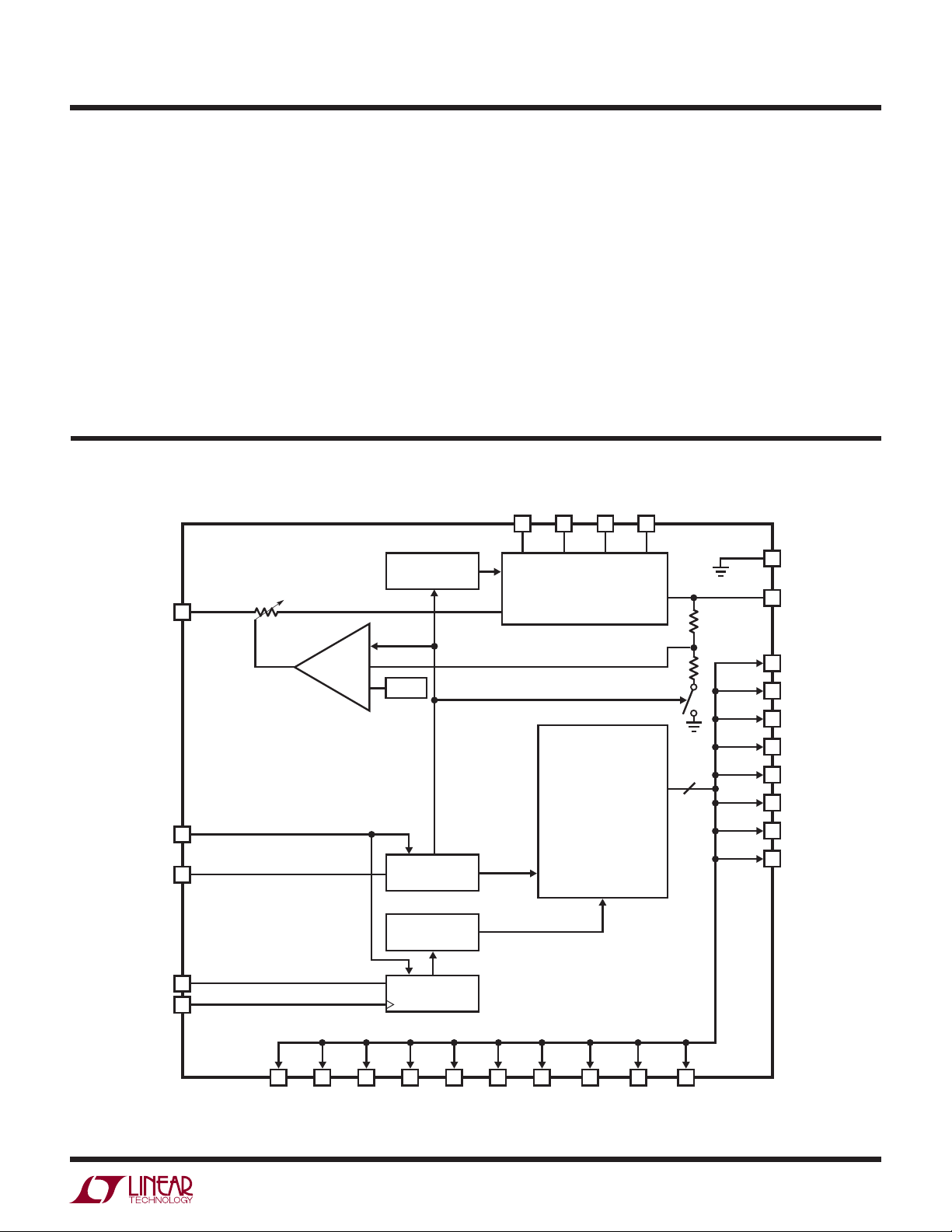
BLOCK DIAGRAM
850kHz
OSCILLATOR
V
IN
24
RST (Pin 25): Active Low Reset Input. RST Resets all
internal registers and forces LTC3220/LTC3220-1 into
shutdown mode.
CPO (Pin 28): Output of the Charge Pump. Used to power
all LEDs. A 4.7μF X5R or X7R ceramic capacitor should
be connected to ground.
Exposed Pad (Pin 29): Ground. The Exposed Pad must
be soldered to PCB ground.
2223 2627
C2MC1M C2PC1P
CHARGE PUMP
EXPOSED
PAD
CPO
29
28
ULED9
9
ULED1
ULED2
ULED3
ULED4
ULED5
ULED6
ULED7
ULED8
1
2
3
4
5
6
7
8
3220 BD
–
+
1.22V
18
18 UNIVERSAL
DV
CC
10
RST
25
SDA
12
SCL
11
ULED17
ULED18
19
20
21
MASTER/SLAVE
SHIFT REGISTER
ULED16
18
CONTROL
LOGIC
REG
ULED15
ULED14
17
ULED13
16
CURRENT SOURCES
AND DACS
ULED12
15
14
ULED11
ULED10
13
32201fb
7

LTC3220/LTC3220-1
OPERATION
Power Management
The LTC3220/LTC3220-1 use a switched capacitor charge
pump to boost CPO as much as 2 times the input voltage
up to 5.1V. The part starts up in 1x mode. In this mode,
is connected directly to CPO. This mode provides
V
IN
maximum effi ciency and minimum noise. The LTC3220/
LTC3220-1 will remain in 1x mode until an LED current
source drops out. Dropout occurs when a current source
voltage becomes too low for the programmed current
to be supplied. When dropout is detected, the LTC3220/
LTC3220-1 will switch into 1.5x mode. The CPO voltage
will then start to increase and will attempt to reach 1.5×
up to 4.6V. Any subsequent dropout will cause the
V
IN
part to enter the 2x mode. The CPO voltage will attempt
to reach 2× V
up to 5.1V.
IN
A 2-phase non-overlapping clock activates the charge
pump switches. In the 2x mode the fl ying capacitors are
charged on alternate clock phases from V
to minimize
IN
CPO voltage ripple. In 1.5x mode the fl ying capacitors are
charged in series during the fi rst clock phase and stacked
in parallel on V
during the second phase. This sequence
IN
of charging and discharging the fl ying capacitors continues
at a constant frequency of 850kHz.
The current delivered by each LED current source is controlled by an associated DAC. Each DAC is programmed
2
via the I
C port.
Soft-Start
Initially, when the part is in shutdown, a weak switch
connects V
to CPO. This allows VIN to slowly charge the
IN
CPO output capacitor and prevent large charging currents
from occurring.
The LTC3220/LTC3220-1 also employ a soft-start feature
on the charge pump to prevent excessive inrush current
and supply droop when switching into the step-up modes.
The current available to the CPO pin is increased linearly
over a typical period of 125μs. Soft-start occurs at the
start of both 1.5x and 2x mode changes.
Charge Pump Strength
When the LTC3220/LTC3220-1 operate in either 1.5x mode
or 2x mode, the charge pump can be modeled as a Thevenin-equivalent circuit to determine the amount of current
available from the effective input voltage and effective
open-loop output resistance, R
is dependent on a number of factors including the
R
OL
switching term, 1/(2f
OSC
• C
(Figure 1).
OL
), internal switch resis-
FLY
tances and the non-overlap period of the switching circuit.
However, for a given R
, the amount of current available
OL
will be directly proportional to the advantage voltage of
– CPO for 1.5x mode and 2VIN – CPO for 2x mode.
1.5V
IN
Consider the example of driving LEDs from a 3.1V supply.
8
R
OL
1.5VIN OR
+
–
2V
IN
Figure 1. Charge Pump Open-Loop Thevenin Equivalent Circuit
+
CPO
–
3220 F01
32201fb

OPERATION
LTC3220/LTC3220-1
If the LED forward voltage is 3.8V and the current sources
require 100mV, the advantage voltage for 1.5x mode is
3.1V • 1.5 – 3.8V – 0.1V or 750mV. Notice that if the input
voltage is raised to 3.2V, the advantage voltage jumps to
900mV, a 20% improvement in available strength.
From Figure 1, for 1.5x mode the available current is
given by:
I
1.5VIN− V
=
OUT
CPO
R
OL
(1)
For 2x mode, the available current is given by:
I
2VIN− V
=
OUT
CPO
R
OL
(2)
Notice that the advantage voltage in this case is 3.1V • 2
– 3.8V – 0.1V = 2.3V. R
is higher in 2x mode but a sig-
OL
nifi cant overall increase in available current is achieved.
Mode Switching
The LTC3220/LTC3220-1 will automatically switch from
1x mode to 1.5x mode and subsequently to 2x mode
whenever a dropout condition is detected at an LED pin.
Dropout occurs when a current source voltage becomes
too low for the programmed current to be supplied. The
mode change will not occur unless dropout exists for approximately 400μs.
The mode will automatically switch back to 1x whenever
2
a register is updated via the I
C port, when gradation
completes ramping down and after each blink period.
The parts can be forced to operate in 1x, 1.5x or 2x mode
by writing the appropriate bits into REG0. This feature may
be used for operating loads powered by CPO.
Non-programmed current sources do not affect dropout.
Universal Current Sources (ULED1 to ULED18)
There are eighteen universal 20mA current sources. Each
current source has a 6-bit linear DAC for current control.
The output current range is 0mA to 20mA in 64 steps.
Each current source is disabled when an all zero data word
is written. The supply current for that source is reduced to
zero. Unused outputs should be connected to GND.
GPO Mode
ULED1 to ULED18 can be used as general purpose outputs
(GPO). Current sources in the GPO mode can be used as
2
C controlled open-drain drivers. A ULED output can be
I
selected to operate in GPO mode by programming both
Bit 6 and Bit 7 of its data register (REG1 to REG18) to a
logic high. In the GPO mode, dropout detection is disabled and output swings to ground will not cause mode
switching.
The GPOs can be programmed to either act as a switch
(strong pull-down mode) in which the part will only consume approximately 3μA of quiescent current, or they can
be programmed to have a regulated current of up to 20mA
(current limit mode), which would require several hundred
microamps of additional quiescent current.
When a ULED output is used in GPO mode during shutdown, CPO should not be used as a power source since
the current available from the CPO pin would be limited
by the weak pull-up current source. This weak pull-up is
only meant to keep the output capacitor charged to V
IN
during shutdown and is unable to supply large amounts
of current. CPO can, however, be used as a power source
when the part is enabled.
Conversely, when a ULED output is used in GPO strong
pull-down mode, a current limiting resistor should be used
in series with the ULED output so that the current does
not exceed the Absolute Maximum rated current.
32201fb
9

LTC3220/LTC3220-1
OPERATION
Blinking
Each universal output (ULED1 to ULED18) can be set to
blink with an on time of 0.156 seconds, or 0.625 seconds
and a period of 1.25 seconds, or 2.5 seconds via the I
port. The blinking rate is selected via REG19 and ULED
outputs are selected via REG1 to REG18. Blinking and
gradation rates are independent. Please refer to Application Note 115 for detailed information and examples on
programming blinking.
Gradation
Universal LED outputs ULED1 to ULED18 can be set to
have the current ramp up and down at 0.24 seconds, 0.48
seconds and 0.96 seconds rates via the I
these outputs can have either blinking or gradation enabled.
The gradation time is set via REG19 and ULED outputs
are selected via REG1 to REG18. The ramp direction is
also controlled via REG19. Setting the up bit high causes
gradation to ramp up, setting this bit to a low causes
gradation to ramp down. Please refer to Application Note
115 for detailed information and examples on programming gradation.
When gradation is disabled the LED output current remains
at the programmed value.
The charge pump mode is reset to 1x mode after gradation
completes ramping down.
Chip Reset (RST)
The RST pin is used to turn off the chip, including the charge
pump and all ULED outputs, and clear all registers in the
2
C port. Each of
2
C
LTC3220/LTC3220-1. When RST is low, the part is in shutdown and cannot be programmed through the I
Shutdown Current
Shutdown occurs when all the current source data bits
have been written to zero, when the shutdown bit in REG0
is written with a logic 1, when RST is pulled low, or when
is set below the undervoltage lockout voltage.
DV
CC
Although the LTC3220/LTC3220-1 are designed to have
very low shutdown current, they will draw about 3μA
from V
the LTC3220/LTC3220-1 are in shutdown when DV
low. Note, however that all of the logic signals that are
referenced to DV
at DV
absolute maximum specifi cations on these pins.
EMI Reduction
The fl ying capacitor pins C1M, C1P, C2M and C2P have
controlled slew rates to reduce conducted and radiated
noise.
Serial Port
The microcontroller compatible I
all of the command and control inputs for the LTC3220/
LTC3220-1. Data on the SDA input is loaded on the rising
edge of SCL. D7 is loaded fi rst and D0 last. There are
20 data registers, one address register and one sub-address register. Once all address bits have been clocked
into the address register, an acknowledge occurs. The
when in shutdown. Internal logic ensures that
IN
(SCL, SDA and RST) will need to be
CC
or below (i.e., ground) to avoid violation of the
CC
2
C serial port provides
2
C port.
CC
is
10
32201fb

OPERATION
LTC3220/LTC3220-1
sub-address register is then written to, followed by the
data register. Each data register has a sub-address. After
the data register has been written a load pulse is created
after the stop bit. The load pulse transfers all of the data
held in the data registers to the DAC registers. The stop
bit can be delayed until all of the data master registers
have been written. At this point the LED current will be
changed to the new settings. The serial port uses static
logic registers so there is no minimum speed at which it
can be operated.
2
C Interface
I
The LTC3220/LTC3220-1 communicate with a host (master)
2
using the standard I
C 2-wire interface. The Timing Diagram
(Figure 3) shows the timing relationship of the signals on
the bus. The two bus lines, SDA and SCL, must be high
LTC3220 WR
00111000
LTC3220-1
00111010
ADDRESS
ADDRESS WR
S7 S6 S5 S4 S3 S2 S1 S0
SUB-ADDRESS
when the bus is not in use. External pull-up resistors or
current sources, such as the LTC1694 SMBus accelerator,
are required on these lines.
The LTC3220/LTC3220-1 are receive-only (slave) devices.
2
There are two I
address is 0011100 and the LTC3220-1 I
0011101. The I
C addresses available. The LTC3220 I2C
2
2
C address is the only difference between
C address is
the LTC3220 and LTC3220-1.
Write Word Protocol Used By the LTC3220/LTC3220-1
17118 1811
S Slave Address Wr A
*Sub-Address
S = Start Condition, Wr = Write Bit = 0, A = Acknowledge,
P = Stop Condition
*The sub-address uses only the fi rst 5 bits, D0, D1, D2, D3 and D4.
**Stop can be delayed until all of the data registers have been written.
DATA BYTE
76543210
A Data Byte A P**
SDA
SCL
00111 000
123
456789123456789123456789
SDA
t
SU, DAT
t
HIGH
t
r
SCL
t
HD, STA
START
CONDITION
t
LOW
ACK
S7 S6 S5 S4 S3 S2 S1 S0
Figure 2. Bit Assignments
t
HD, DAT
t
f
REPEATED START
CONDITION
Figure 3. Timing Parameters
t
SU, STA
t
HD, STA
STOPSTART
ACK
76543210
t
BUF
t
SU, STO
3220 F03
t
SP
STOP
CONDITION
START
CONDITION
ACK
3220 FO2
32201fb
11

LTC3220/LTC3220-1
OPERATION
Sub-Address Byte
MSB LSB
7 6 5 4 3 2 1 0 Register Function
0 0 0 0 0 0 0 0 REG0 COMMAND
00000001REG1 ULED1
00000010REG2 ULED2
00000011REG3 ULED3
00000100REG4 ULED4
00000101REG5 ULED5
00000110REG6 ULED6
00000111REG7 ULED7
00001000REG8 ULED8
00001001REG9 ULED9
0 0 0 0 1 0 1 0 REG10 ULED10
00001011REG11ULED11
00001100REG12ULED12
00001101REG13ULED13
00001110REG14ULED14
00001111REG15ULED15
00010000REG16ULED16
00010001REG17ULED17
00010010REG18ULED18
00010011REG19 GRAD/
BLINK
REG0, Command Byte.
Register Sub-Address = 0000
MSB LSB
D7 D6 D5 D4 D3 D2 D1 D0
Unused Unused Unused Unused Shutdown Force2x Force1p5x Quick write
Quick write 01Serial write to each register
Force1p5 10Forces charge pump into 1.5x mode
Force2x 10Forces charge pump into 2x mode
Force1x D2 (Force1p5x) = 1
Shutdown 10Shuts down part while preserving data in registers
Parallel write, REG1 data is written to all eighteen universal registers
Enables mode logic to control mode changes based on dropout signal
Enables mode logic to control mode changes based on dropout signal
D3 (Force2x) = 1
Normal operation
Forces Charge Pump into 1x Mode
32201fb
12

OPERATION
Data Bytes
REG1 to REG18, Universal LED 6-bit linear DAC data with
blink/gradation.
Sub-Address 00001 to 10010 per Sub-Address Table
Blink/Gradation/Dropout Enable LED Current Data
MSB LSB
Bit 7 Bit 6 Bit 5 Bit 4 Bit 3 Bit 2 Bit 1 Bit 0
Normal
Blink Enabled
Gradation Enabled
GPO Mode*
Strong Pull-Down Mode
Current Limited Mode
High Impedance/Off
*(Gradation/Blink/Dropout Off)
0
0
1
1
1
0
0
1
0
1
1
0
D5
D5
D5
0
D5
0
D4
D4
D4
D4
LTC3220/LTC3220-1
D3
D3
D3
0
0
0
D3
0
D2
D2
D2
0
D2
0
D1
D1
D1
0
D1
0
D0
D0
D0
0
D0
0
REG19, Gradation and Blinking
MSB LSB
D7 D6 D5 D4 D3 D2 D1 D0
Unused Unused Unused GB4 GB3 GB2 GB1 Up
Up 0
1
Blink Times and Period Gradation Ramp Times and Period
D4 (GB4) D3 (GB3) On Time Period D2 (GB2) D1 (GB1) Ramp Time Period
0
0
1
1
Gradation counts down
Gradation counts up
0
1
0
1
0.625s
0.156s
0.625s
0.156s
1.25s
1.25s
2.5s
2.5s
0
0
1
1
0
1
0
1
Disabled
0.24s
0.48s
0.96s
Disabled
0.313s
0.625s
1.25s
32201fb
13

LTC3220/LTC3220-1
OPERATION
Bus Speed
2
C port is designed to be operated at speeds up to
The I
400kHz. It has built-in timing delays to ensure correct
operation when addressed from an I
device. It also contains input fi lters designed to suppress
glitches should the bus become corrupted.
Start and Stop Conditions
A bus-master signals the beginning of a communication
to a slave device by transmitting a Start condition.
A Start condition is generated by transitioning SDA from
high to low while SCL is high. When the master has
fi nished communicating with the slave, it issues a Stop
condition by transitioning SDA from low to high while
SCL is high. The bus is then free for communication with
another I
Byte Format
Each byte sent to the LTC3220/LTC3220-1 must be 8 bits
long followed by an extra clock cycle for the Acknowledge
bit to be returned by the LTC3220/LTC3220-1. The data
should be sent to the LTC3220/LTC3220-1 most signifi cant
bit (MSB) fi rst.
2
C device.
2
C compliant master
Acknowledge
The Acknowledge signal is used for handshaking between
the master and the slave. An Acknowledge (active low)
generated by the slave (LTC3220/LTC3220-1) lets the master know that the latest byte of information was received.
The Acknowledge related clock pulse is generated by the
master. The master releases the SDA line (high) during
the Acknowledge clock cycle. The slave-receiver must pull
down the SDA line during the Acknowledge clock pulse
so that it remains a stable low during the high period of
this clock pulse.
Slave Address
Each version of LTC3220/LTC3220-1 responds to a unique
address which has been factory programmed (Table 1).
The eighth bit of the address byte (R/W) must be 0 for the
LTC3220/LTC3220-1 to recognize the address since it is a
write only device. This effectively forces the address to be
8 bits long where the least signifi cant bit of the address
is 0. If the correct seven bit address is given but the R/W
bit is 1, the LTC3220/LTC3220-1 will not respond.
Table 1. LTC3220/LTC3220-1 Factory Programmed Slave
Address
PART NUMBER SLAVE ADDRESS
LTC3220 0011100
LTC3220-1 0011101
14
32201fb

OPERATION
LTC3220/LTC3220-1
Bus Write Operation
The master initiates communication with the LTC3220/
LTC3220-1 with a Start condition and a 7-bit address followed by the Write Bit R/W = 0. If the address matches
that of the LTC3220/LTC3220-1, the LTC3220/LTC3220-1
return an Acknowledge. The master should then deliver the
most signifi cant sub-address byte for the data register to
be written. Again the LTC3220/LTC3220-1 acknowledge and
then the data is delivered starting with the most signifi cant
bit. This cycle is repeated until all of the required data registers have been written. Any number of data latches can be
written. Each data byte is transferred to an internal holding
latch upon the return of an Acknowledge. After all data
bytes have been transferred to the LTC3220/LTC3220-1,
the master may terminate the communication with a Stop
condition. Alternatively, a Repeat-Start condition can be
initiated by the master and another chip on theI
be addressed. This cycle can continue indefi nitely and the
LTC3220/LTC3220-1 will remember the last input of valid
data that it received. Once all chips on the bus have been
addressed and sent valid data, a global Stop condition
can be sent and the LTC3220/LTC3220-1 will update all
registers with the data that it had received.
2
C bus can
In certain circumstances the data on the I2C bus may become corrupted. In these cases the LTC3220/LTC3220-1
respond appropriately by preserving only the last set of
complete data that it has received. For example, assume
the LTC3220/LTC3220-1 has been successfully addressed
and is receiving data when a Stop condition mistakenly
occurs. The LTC3220/LTC3220-1 will ignore this Stop
condition and will not respond until a new Start condition,
correct address, sub-address and new set of data and Stop
condition are transmitted.
Likewise, if the LTC3220/LTC3220-1 were previously addressed and sent valid data but not updated with a Stop,
they will respond to any Stop that appears on the bus with
only one exception, independent of the number of RepeatStart’s that have occurred. If a Repeat-Start is given and
the LTC3220/LTC3220-1 successfully acknowledge their
addresses and fi rst byte, they will not respond to a Stop
until all bytes of the new data have been received and
acknowledged.
Quick Write
Registers REG1 to REG18 can be written in parallel by setting Bit 0 of REG 0 high. When this bit is set high the next
write sequence to REG1 will write the data to REG1 through
REG18, which are all of the universal LED registers.
32201fb
15
LTC3220/LTC3220-1
APPLICATIONS INFORMATION
VIN, CPO Capacitor Selection
The style and value of the capacitors used with the LTC3220/
LTC3220-1 determine several important parameters such
as regulator control loop stability, output ripple, charge
pump strength and minimum start-up time.
To reduce noise and ripple, it is recommended that low
equivalent series resistance (ESR) ceramic capacitors are
used for both C
VIN
and C
. Tantalum and aluminum
CPO
capacitors are not recommended due to high ESR.
The value of C
ripple for a given load current. Increasing the size of C
directly controls the amount of output
CPO
CPO
will reduce output ripple at the expense of higher start-up
current. The peak-to-peak output ripple of the 1.5x mode
is approximately given by the expression:
I
V
RIPPLEP-P
where f
=
is the LTC3220/LTC3220-1 oscillator fre-
OSC
OUT
3f
OSC•CCPO
quency or typically 850kHz and C
is the output storage
CPO
(3)
capacitor.
The output ripple in 2x mode is very small due to the fact
that load current is supplied on both cycles of the clock.
Both type and value of the output capacitor can signifi cantly
affect the stability of the LTC3220/LTC3220-1. As shown in
the Block Diagram, the LTC3220/LTC3220-1 use a control
loop to adjust the strength of the charge pump to match
the required output current. The error signal of the loop is
stored directly on the output capacitor. The output capacitor
also serves as the dominant pole for the control loop. To
prevent ringing or instability, it is important for the output
capacitor to maintain at least 3.2μF of capacitance over all
conditions and the ESR should be less than 80mΩ.
Multilayer ceramic chip capacitors typically have exceptional ESR performance. MLCCs combined with a tight
board layout will result in very good stability. As the value
of C
of C
pin (V
controls the amount of output ripple, the value
CPO
controls the amount of ripple present at the input
VIN
). The LTC3220/LTC3220-1 input current will be
IN
relatively constant while the charge pump is either in the
input charging phase or the output charging phase but will
drop to zero during the clock nonoverlap times. Since the
nonoverlap time is small (~25ns), these missing “notches”
will result in only a small perturbation on the input power
supply line. Note that a higher ESR capacitor such as tantalum will have higher input noise due to the higher ESR.
Therefore, ceramic capacitors are recommended for low
ESR. Input noise can be further reduced by powering the
LTC3220/LTC3220-1 through a very small series inductor
as shown in Figure 4. A 10nH inductor will reject the fast
current notches, thereby presenting a nearly constant
current load to the input power supply. For economy, the
10nH inductor can be fabricated on the PC board with
about 1cm (0.4") of PC board trace.
16
V
BAT
LTC3220
LTC3220-1
GND
3220 F04
Figure 4. 10nH Inductor Used for Input Noise Reduction
(Approximately 1cm of Board Space)
32201fb
APPLICATIONS INFORMATION
LTC3220/LTC3220-1
Flying Capacitor Selection
Warning: Polarized capacitors such as tantalum or
aluminum should never be used for the fl ying capacitors since their voltage can reverse upon start-up of the
LTC3220/LTC3220-1. Ceramic capacitors should always
be used for the fl ying capacitors.
The fl ying capacitors control the strength of the charge
pump. In order to achieve the rated output current it is
necessary to have at least 1.6μF of capacitance for each of
the fl ying capacitors. Capacitors of different materials lose
their capacitance with higher temperature and voltage at
different rates. For example, a ceramic capacitor made of
X7R material will retain most of its capacitance from –40°C
to 85°C, whereas a Z5U or Y5V style capacitor will lose
considerable capacitance over that range. Z5U and Y5V
capacitors may also have a very poor voltage coeffi cient
causing them to lose 60% or more of their capacitance when
the rated voltage is applied. Therefore, when comparing
different capacitors, it is often more appropriate to compare
the amount of achievable capacitance for a given case size
rather than comparing the specifi ed capacitance value. For
example, over rated voltage and temperature conditions,
a 1μF, 10V, Y5V ceramic capacitor in a 0603 case may not
provide any more capacitance than a 0.22μF, 10V, X7R
available in the same case. The capacitor manufacturer’s
data sheet should be consulted to determine what value
of capacitor is needed to ensure minimum capacitances
at all temperatures and voltages.
Table 2 shows a list of ceramic capacitor manufacturers
and how to contact them:
Table 2. Recommended Capacitor Vendors
AVX www.avxcorp.com
Kemet www.kemet.com
Murata www.murata.com
Taiyo Yuden www.t-yuden.com
Vishay www.vishay.com
Layout Considerations and Noise
The LTC3220/LTC3220-1 have been designed to minimize
EMI. However due to their high switching frequency and the
transient currents produced by the LTC3220/LTC3220-1,
careful board layout is necessary. A true ground plane
and short connections to all capacitors will improve
performance and ensure proper regulation under all
conditions.
The fl ying capacitor pins C1P, C2P, C1M and C2M have
controlled edge rate waveforms. The large dv/dt on these
pins can couple energy capacitively to adjacent PCB runs.
Magnetic fi elds can also be generated if the fl ying capacitors are not close to the LTC3220/LTC3220-1 (i.e., the loop
area is large). To decouple capacitive energy transfer, a
Faraday shield may be used. This is a grounded PCB trace
between the sensitive node and the LTC3220/LTC3220-1
pins. For a high quality AC ground, it should be returned
to a solid ground plane that extends all the way to the
LTC3220/LTC3220-1.
32201fb
17

LTC3220/LTC3220-1
APPLICATIONS INFORMATION
Power Effi ciency
To calculate the power effi ciency (η) of an LED driver chip,
the LED power should be compared to the input power.
The difference between these two numbers represents
lost power whether it is in the charge pump or the current sources. Stated mathematically, the power effi ciency
is given by:
P
LED
η=
P
IN
(4)
The effi ciency of the LTC3220/LTC3220-1 depends upon
the mode in which it is operating. Recall that the LTC3220/
LTC3220-1 operate as pass switches, connecting VIN to
CPO, until dropout is detected at the I
pin. This feature
LED
provides the optimum effi ciency available for a given input
voltage and LED forward voltage. When it is operating as
a switch, the effi ciency is approximated by:
P
η=
P
LED
IN
V
LED•ILED
=
VIN•I
V
LED
=
IN
V
IN
(5)
since the input current will be very close to the sum of
the LED currents.
At moderate to high output power, the quiescent current
of the LTC3220/LTC3220-1 is negligible and the expression above is valid.
Once dropout is detected at any LED pin, the LTC3220/
LTC3220-1 enable the charge pump in 1.5x mode.
In 1.5x boost mode, the effi ciency is similar to that of a
linear regulator with an effective input voltage of 1.5 times
the actual input voltage. This is because the input current
for a 1.5x charge pump is approximately 1.5 times the
load current. In an ideal 1.5x charge pump, the power
effi ciency would be given by:
P
η
IDEAL
LED
=
P
IN
V
LED•ILED
=
VIN• 1.5 •I
LED
=
1.5 • V
V
LED
IN
Similarly, in 2x boost mode, the effi ciency is similar to
that of a linear regulator with an effective input voltage
of 2 times the actual input voltage. In an ideal 2x charge
pump, the power effi ciency would be given by:
P
η
IDEAL
LED
=
P
IN
V
LED•ILED
=
VIN•2•I
LED
=
V
LED
2•V
IN
Thermal Management
For higher input voltages and maximum output current,
there can be substantial power dissipation in the LTC3220/
LTC3220-1. If the junction temperature increases above
approximately 150°C, the thermal shutdown circuitry will
automatically deactivate the output current sources and
charge pump. To reduce maximum junction temperature,
a good thermal connection to the PC board is recommended. Connecting the Exposed Pad to a ground plane
and maintaining a solid ground plane under the device
will reduce the thermal resistance of the package and PC
board considerably.
18
32201fb
PACKAGE DESCRIPTION
2.64 ± 0.05
4.50 ± 0.05
2.40 REF
3.10 ± 0.05
RECOMMENDED SOLDER PAD PITCH AND DIMENSIONS
APPLY SOLDER MASK TO AREAS THAT ARE NOT SOLDERED
4.00 ± 0.10
2.64 ± 0.05
4.00 ± 0.10
PIN 1
TOP MARK
(NOTE 6)
PF Package
28-Lead UTQFN (4mm × 4mm)
(Reference LTC DWG # 05-08-1759 Rev Ø)
0.70 ±0.05
PACKAGE OUTLINE
0.20 ±0.05
0.40 BSC
0.55 ± 0.05
R = 0.05
TYP
2.40 REF
LTC3220/LTC3220-1
BOTTOM VIEW—EXPOSED PAD
R = 0.10
TYP
2.64 ± 0.10
2827
PIN 1 NOTCH
R = 0.20 TYP
OR 0.25 × 45°
CHAMFER
0.40 ± 0.5
1
2
2.64 ± 0.10
NOTE:
1. DRAWING IS NOT A JEDEC PACKAGE OUTLINE
2. DRAWING NOT TO SCALE
3. ALL DIMENSIONS ARE IN MILLIMETERS
4. DIMENSIONS OF EXPOSED PAD ON BOTTOM OF PACKAGE DO NOT INCLUDE
MOLD FLASH. MOLD FLASH, IF PRESENT, SHALL NOT EXCEED 0.15mm ON ANY SIDE, IF PRESENT
5. EXPOSED PAD SHALL BE SOLDER PLATED
6. SHADED AREA IS ONLY A REFERENCE FOR PIN 1 LOCATION
ON THE TOP AND BOTTOM OF PACKAGE
0.127 REF
0.00 – 0.05
(PF28) UTQFN 0907
0.20 ± 0.05
0.40 BSC
32201fb
Information furnished by Linear Technology Corporation is believed to be accurate and reliable.
However, no responsibility is assumed for its use. Linear Technology Corporation makes no representation that the interconnection of its circuits as described herein will not infringe on existing patent rights.
19
LTC3220/LTC3220-1
TYPICAL APPLICATION
Cellular Phone Multi-Display LED Controller with Auxiliary Current Source Output
2.2μF 2.2μF
C1M
LTC3220
C2M
C2P
CPO
ULED1-18
4.7μF
18
V
IN
DV
CC
2.2μF
0.1μF
C1P
V
DV
IN
CC
LTC3220-1
CAM
MAIN RGB
BLINKING
STATUS
INDICATORS
GPO 1, 2, 3 V
60mA
3220 TA02
IN
100k
GPO4
I2C
SCL/SDA
RST
GND
RELATED PARTS
PART NUMBER DESCRIPTION COMMENTS
LTC3205 250mA, 1MHz, Multi-Display LED Controller V
LTC3206 400mA, 800kHz, Multi-Display LED Controller V
LTC3207 600mA Universal Multi-Output LED/CAM Driver V
: 2.8V to 4.5V, V
IN
: 2.8V to 4.5V, V
IN
: 2.9V to 5.5V, 12 Universal Individually Controlled LED Drivers, One
BAT
Camera Driver, 4mm × 4mm QFN Package
LTC3208 High Current Software Confi gurable Multi-Display
LED Controller
LTC3209-1/
600mA MAIN/Camera/AUX LED Controller V
LTC3209-2
LTC3210 MAIN/CAM LED Controller in 3mm × 3mm QFN V
: 2.9V to 4.5V, V
V
IN
(MAIN, SUB, RGB, CAM, AUX), 5mm × 5mm QFN Package
: 2.9V to 4.5V, IQ = 400mA, Up to 94% Effi ciency, 4mm × 4mm
IN
QFN-20 Package
: 2.9V to 4.5V, IQ = 400μA, 3-Bit DAC Brightness Control for MAIN and CAM
IN
LEDs, 3mm × 3mm QFN Package
LTC3210-1 MAIN/CAM LED Controller with 64-Step
Brightness Control
LTC3210-2 MAIN/CAM LED Controller with 32-Step
6-Bit DAC Brightness Control for MAIN and 3-Bit Brightness Control for CAM,
3mm × 3mm QFN Package
Drives 4 MAIN LEDs, 3mm × 3mm QFN Package
Brightness Control
LTC3210-3 MAIN/CAM LED Controller with 32-Step
Drives 3 MAIN LEDs, 3mm × 3mm QFN Package
Brightness Control
LTC3212 RGB LED Driver and Charge Pump Drives RGB LEDs, 25mA/LED × 3, V
Package
LTC3214 500mA Camera LED Charge Pump V
LTC3215 700mA Low Noise High Current LED
: 2.9V to 4.5V, Single Output, 3mm × 3mm DFN Package
IN
: 2.9V to 4.4V, V
V
IN
Charge Pump
LTC3216 1A Low Noise High Current LED Charge Pump
: 2.9V to 4.4V, V
V
IN
with Independent Flash/Torch Current Control
LTC3217 600mA Low Noise Multi-LED Camera Light V
: 2.9V to 4.4V, IQ = 400μA, Four 100mA Outputs, QFN Package
IN
LTC3218 400mA Single-Wire Camera LED Charge Pump 91% Effi ciency, VIN Range: 2.9V to 4.5V, 2mm × 3mm DFN Package,
High Side Current Sense
LTC3219 250mA Universal Multi-Output LED Driver V
2.9V to 5.5V, Nine Universal Individually Controlled LED Drivers,
BAT
3mm × 3mm QFN Package
LTC3440/LTC3441 600mA/1.2A I
Buck-Boost DC/DC Converter
LTC3443 600mA/1.2A I
, 2MHz/1MHz, Synchronous
OUT
, 600kHz, Synchronous
OUT
VIN: 2.4V to 5.5V, V
MS/DFN Packages
VIN: 2.4V to 5.5V, V
Buck-Boost DC/DC Converter
LTC3453 1MHz, 800mA Synchronous Buck-Boost High
Power LED Driver
: 2.7V to 5.5V, V
V
IN(MIN)
QFN Package
Linear Technology Corporation
20
1630 McCarthy Blvd., Milpitas, CA 95035-7417
(408) 432-1900 ● FAX: (408) 434-0507 ● www.linear.com
= 5.5V, IQ = 50μA, ISD < 1μA, QFN Package
OUT(MAX)
= 5.5V, IQ = 50μA, ISD < 1μA, QFN Package
OUT(MAX)
= 5.5V, IQ = 250μA, ISD < 3μA, 17 Current Sources
OUT(MAX)
Range: 2.9V to 4.5V, 2mm × 3mm DFN
IN
= 5.5V, IQ = 300μA, ISD < 2.5μA, DFN Package
OUT(MAX)
= 5.5V, IQ = 300μA, ISD < 2.5μA, DFN Package
OUT(MAX)
= 5.25V, IQ = 25μA/50μA, ISD <1μA,
OUT(MAX)
= 5.25V, IQ = 28μA, ISD <1μA, DFN Package
OUT(MAX)
: 2.7V to 4.5V, IQ = 2.5mA, ISD < 6μA,
IN(MAX)
LT 0908 REV B • PRINTED IN USA
© LINEAR TECHNOLOGY CORPORATION 2007
32201fb
 Loading...