

LTC3210-2/LTC3210-3
MAIN/CAM LED Controllers
with 32-Step Brightness Control
in 3mm × 3mm QFN
FEATURES DESCRIPTION
■
Low Noise Charge Pump Provides High Effi ciency
with Automatic Mode Switching
■
Multimode Operation: 1x, 1.5x, 2x
■
Individual Full-Scale Current Set Resistors
■
Up to 500mA Total Output Current
■
Single Wire EN/Brightness Control for MAIN and
CAM LEDs
■
32:1 Linear Brightness Control Range for
MAIN Display
■
Three or Four 25mA Low Dropout MAIN LED Outputs
■
One 400mA Low Dropout CAM LED Output
■
Low Noise Constant Frequency Operation*
■
Low Shutdown Current: 3µA
■
Internal Soft-Start Limits Inrush Current During
Startup and Mode Switching
■
Open/Short LED Protection
■
No Inductors
■
3mm × 3mm 16-Lead Plastic QFN Package
APPLICATIONS
■
Multi-LED Light Supply for Cellphones/DSCs/PDAs
, LT, LTC and LTM are registered trademarks of Linear Technology Corporation.
All other trademarks are the property of their respective owners.
*Protected by US Patents including 6411531.
The LTC®3210-2/LTC3210-3 are low noise charge pump
DC/DC converters designed to drive three or four MAIN
LEDs and one high current CAM LED for camera lighting.
The LTC3210-2/LTC3210-3 require only four small ceramic
capacitors and two current set resistors to form a complete
LED power supply and current controller.
Built-in soft-start circuitry prevents excessive inrush current during start-up and mode changes. High switching
frequency enables the use of small external capacitors.
Independent MAIN and CAM full-scale current settings
are programmed by two external resistors.
Shutdown mode and current output levels are selected
via two logic inputs. ENM and ENC are toggled to adjust
the LED currents via internal counters and DACs. A 5-bit
linear DAC (32 steps) provides high resolution brightness
control for the MAIN display.
The charge pump optimizes effi ciency based on the voltage across the LED current sources. The part powers up
in 1x mode and will automatically switch to boost mode
whenever any enabled LED current source begins to enter
dropout. The LTC3210-2/LTC3210-3 are available in a
3mm × 3mm 16-lead QFN package.
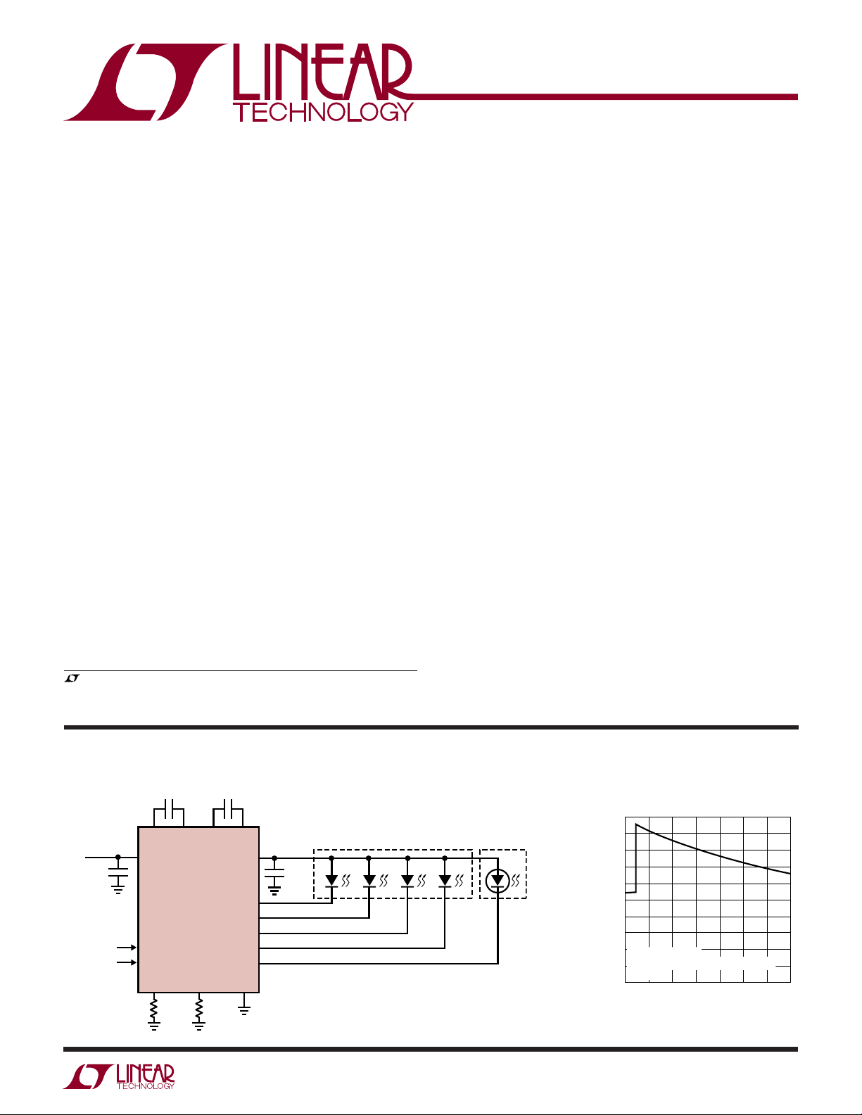
TYPICAL APPLICATION
C2
2.2µF
C1P C1M C2P
V
BAT
C1
2.2µF
ENM
ENC
V
BAT
LTC3210-2
ENM
ENC
RM RC GND
30.1k1%24.3k
1%
C3
2.2µF
C2M
CPO
MLED1
MLED2
MLED3
MLED4
CLED
C4
2.2µF
MAIN CAM
321023 TA01
Effi ciency vs V
100
90
80
) (%)
70
IN
/P
60
LED
50
40
30
EFFICIENCY (P
20
4 LEDs AT 9mA/LED
(TYP V
10
= 25°C
T
A
0
3.0
4-LED MAIN Display
Voltage
BAT
AT 9mA = 3V, NICHIA NSCW100)
F
3.2
3.6
3.4
3.8
BAT
4.0
(V)
V
4.44.2
321023 TA01b
321023f
1
LTC3210-2/LTC3210-3
ABSOLUTE MAXIMUM RATINGS
V
, CPO to GND ........................................–0.3V to 6V
BAT
ENM, ENC ................................... – 0.3V to (V
(Note 2) ........................................................600mA
I
CPO
I
MLED1-4
.................................................................35mA
BAT
(Note 1)
+ 0.3V)
PACKAGE/ORDER INFORMATION
TOP VIEW
BAT
C2P
V
C1M
C2M
16 15 14 13
RM
MLED4
12
GND
CLED
11
ENC
10
RC
9
1C1P
CPO
2
ENM
MLED1
16-LEAD (3mm × 3mm) PLASTIC QFN
T
EXPOSED PAD (PIN 17) IS GND, MUST BE SOLDERED TO PCB
JMAX
17
3
4
5 6 7 8
MLED2
MLED3
UD PACKAGE
= 125°C, θJA = 68°C/W
(Note 2) ......................................................500mA
I
CLED
CPO Short-Circuit Duration .............................. Indefi nite
Operating Temperature Range (Note 3) ...–40°C to 85°C
Storage Temperature Range ...................–65°C to 125°C
TOP VIEW
BAT
C2P
V
C1M
C2M
16 15 14 13
NC
RM
12
GND
CLED
11
ENC
10
RC
9
1C1P
CPO
2
ENM
MLED1
16-LEAD (3mm × 3mm) PLASTIC QFN
T
EXPOSED PAD (PIN 17) IS GND, MUST BE SOLDERED TO PCB
JMAX
17
3
4
5 6 7 8
MLED2
MLED3
UD PACKAGE
= 125°C, θJA = 68°C/W
ORDER PART NUMBER UD PART MARKING ORDER PART NUMBER UD PART MARKING
LTC3210EUD-2 LCHX LTC3210EUD-3 LCHY
Order Options Tape and Reel: Add #TR
Lead Free: Add #PBF Lead Free Tape and Reel: Add #TRPBF
Lead Free Part Marking: http://www.linear.com/leadfree/
Consult LTC Marketing for parts specifi ed with wider operating temperature ranges.
ELECTRICAL CHARACTERISTICS
The
temperature range, otherwise specifi cations are at T
= 25°C.V
A
ENM = high, unless otherwise noted.
PARAMETER CONDITIONS MIN TYP MAX UNITS
Operating Voltage
V
BAT
Operating Current I
I
VBAT
Shutdown Current ENM = ENC = Low
V
BAT
MLED1, MLED2, MLED3 and MLED4 (LTC3210-2 Only) Current
LED Current Ratio (I
MLED/IRM
)I
LED Dropout Voltage
LED Current Matching
MLED Current, 5-Bit Linear DAC 1 ENM Strobe (FS)
= 0, 1x Mode, LSB Setting
CPO
I
= 0, 1.5x Mode
CPO
I
= 0, 2x Mode
CPO
MLED
Mode Switch Threshold, I
Any Two Outputs 0.5 %
31 ENM Strobes (FS/31)
●
denotes the specifi cations which apply over the full operating
BAT
= Full Scale
= 3.6V, C1 = C2 = C3 = C4 = 2.2µF, RM = 30.1k, RC = 24.3k,
●
2.9 4.5 V
0.4
2.5
4.5
= Full Scale
MLED
●
●
481 525 589 A/A
36 µA
75 mV
20
0.640
mA
mA
mA
mA
mA
2
321023f
LTC3210-2/LTC3210-3
The
ELECTRICAL CHARACTERISTICS
temperature range, otherwise specifi cations are at T
= 25°C.V
A
●
denotes the specifi cations which apply over the full operating
= 3.6V, C1 = C2 = C3 = C4 = 2.2µF, RM = 30.1k, RC = 24.3k,
BAT
ENM = high, unless otherwise noted.
PARAMETER CONDITIONS MIN TYP MAX UNITS
CLED Current
LED Current Ratio (I
)I
CLED/IRC
LED Dropout Voltage Mode Switch Threshold, I
= Full Scale
CLED
= Full Scale 500 mV
CLED
CLED Current, 3-Bit Linear DAC 1 ENC Strobe (FS)
7 ENC Strobes (FS/7)
Charge Pump (CPO)
1x Mode Output Voltage I
1.5x Mode Output Voltage I
2x Mode Output Voltage I
= 0mA V
CPO
= 0mA 4.55 V
CPO
= 0mA 5.05 V
CPO
1x Mode Output Impedance 0.55
1.5x Mode Output Impedance V
2x Mode Output Impedance V
= 3.4V, V
BAT
= 3.2V, V
BAT
= 4.6V (Note 4) 3.15
CPO
= 5.1V (Note 4) 3.95
CPO
CLOCK Frequency
Mode Switching Delay 0.4 ms
ENC, ENM
V
IL
V
IH
I
IH
I
IL
ENM = ENC = 3.6V
ENM = ENC = 0V
ENC, ENM Timing
t
PW
t
SD
t
EN
Minimum Pulse Width
Low Time to Shutdown (ENC, ENM = Low)
Current Source Enable Time
(ENC, ENM = High) (Note 5)
RM, RC
V
, V
RM
RC
, I
I
RM
RC
●
6930 7700 8470 A/A
380
54
BAT
0.8 MHz
●
●
1.4 V
●
10 15 20 µA
●
–1 1 µA
●
200 ns
●
50 150 250 µs
50 150 250 µs
●
●
1.16 1.20 1.24 V
●
0.4 V
80 µA
mA
mA
V
Ω
Ω
Ω
Note 1: Stresses beyond those listed under Absolute Maximum Ratings
may cause permanent damage to the device. Exposure to any Absolute
Maximum Rating condition for extended periods may affect device
reliability and lifetime.
Note 2: Based on long-term current density limitations. Assumes an
operating duty cycle of ≤10% under absolute maximum conditions
for durations less than 10 seconds. Maximum current for continuous
operation is 300mA.
Note 3: The LTC3210-2/LTC3210-3 are guaranteed to meet performance
specifi cations from 0°C to 70°C. Specifi cations over the – 40°C to
85°C ambient operating temperature range are assured by design,
characterization and correlation with statistical process controls.
Note 4: 1.5x mode output impedance is defi ned as (1.5V
2x mode output impedance is defi ned as (2V
BAT
– V
CPO
)/I
BAT
OUT
– V
.
CPO
)/I
OUT
.
Note 5: If the part has been shut down then the initial enable time is about
100µs longer due to the bandgap enable time.
321023f
3
LTC3210-2/LTC3210-3
= 25°C unless otherwise stated.
1.5X
T
A
V
BAT
I
2X
50mV/DIV
COUPLED
CPO
C
CPO
V
CPO
AC
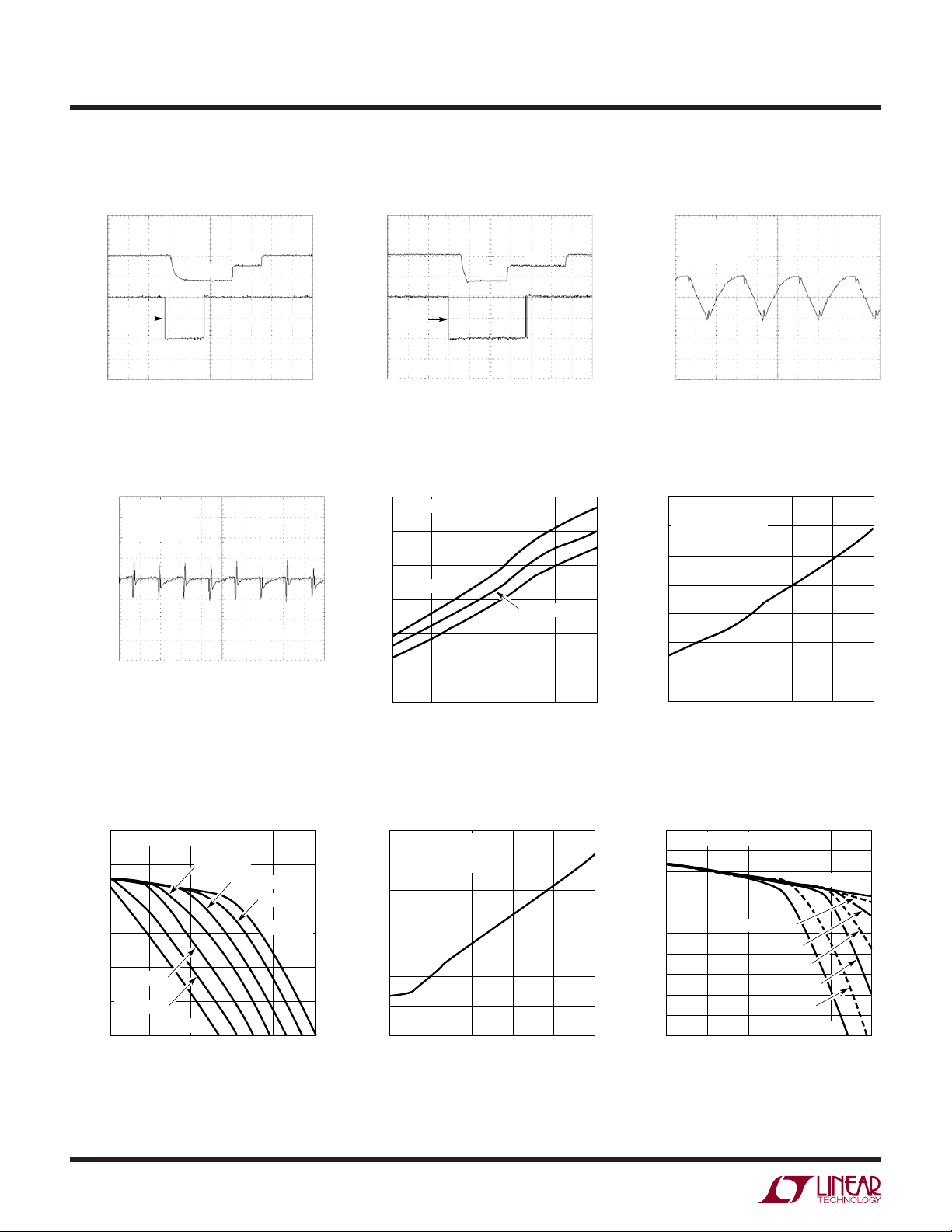
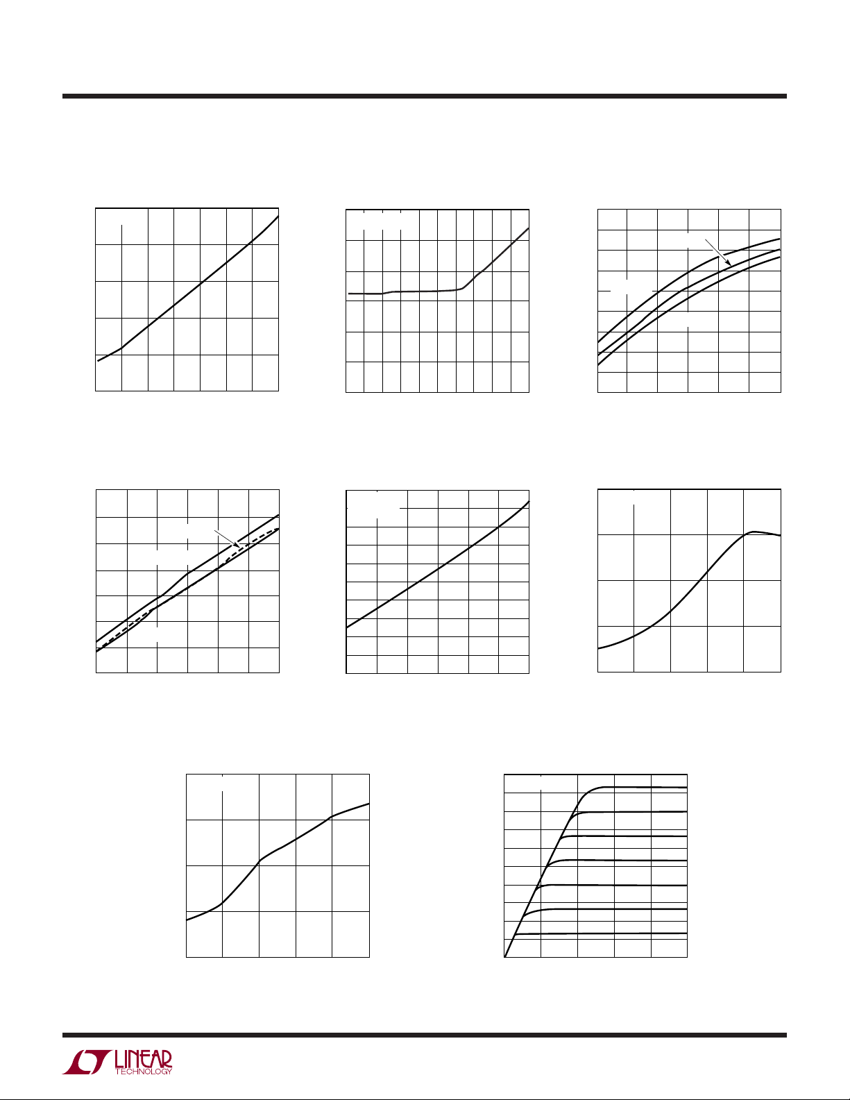
TYPICAL PERFORMANCE CHARACTERISTICS
Dropout Time from Shutdown Dropout Time When Enabled 1.5x CPO Ripple
MODE
RESET
5.1V
1X
CPO
1V/DIV
2V/DIV
5.1V
1X
EN
MODE
RESET
1.5X
2X
CPO
1V/DIV
ENC
2V/DIV
= 3.6V
= 200mA
= 2.2µF
2x CPO Ripple
V
= 3.6V
BAT
= 200mA
I
CPO
= 2.2µF
C
CPO
V
CPO
20mV/DIV
AC
COUPLED
1.5x Mode CPO Voltage
vs Load Current
4.8
C2 = C3 = C4 = 2.2µF
4.6
4.4
4.2
4.0
CPO VOLTAGE (V)
V
= 3.2V
BAT
3.8
V
= 3.1V
BAT
3.6
0
V
100 200 300 400
500µs/DIV
500ns/DIV
V
= 3.3V
BAT
V
BAT
= 3V
BAT
LOAD CURRENT (mA)
= 3.4V
V
BAT
V
BAT
321023 G01
321023 G04
= 3.5V
= 3.6V
321023 G07
500
ENM = HIGH
250µs/DIV
1x Mode Switch Resistance
vs Temperature
0.70
I
= 200mA
CPO
0.65
0.60
V
= 3.3V
0.55
0.50
SWITCH RESISTANCE (Ω)
0.45
0.40
BAT
V
= 3.9V
BAT
–40
–15 10 35 60
TEMPERATURE (°C)
V
BAT
2x Mode Charge Pump Open-Loop
Output Resistance vs Temperature
– V
(2V
4.6
V
BAT
V
CPO
4.4
C2 = C3 = C4 = 2.2µF
4.2
4.0
3.8
3.6
3.4
OPEN-LOOP OUTPUT RESISTANCE (Ω)
3.2
–40
BAT
= 3V
= 4.8V
–15 10 35 85
)/I
CPO
CPO
TEMPERATURE (°C)
= 3.6V
60
321023 G02
321023 G05
321023 G08
85
500ns/DIV
1.5x Mode Charge Pump Open-Loop
Output Resistance vs Temperature
– V
(1.5V
3.8
V
BAT
V
CPO
3.6
C2 = C3 = C4 = 2.2µF
3.4
3.2
3.0
2.8
2.6
OPEN-LOOP OUTPUT RESISTANCE (Ω)
2.4
–40
BAT
= 3V
= 4.2V
–15 10 35 85
)/I
CPO
CPO
TEMPERATURE (°C)
2x Mode CPO Voltage
vs Load Current
5.2
C2 = C3 = C4 = 2.2µF
5.1
5.0
4.9
4.8
4.7
4.6
CPO VOLTAGE (V)
4.5
4.4
4.3
4.2
0
V
BAT
V
BAT
V
100
200
LOAD CURRENT (mA)
= 3.5V
= 3.4V
BAT
V
BAT
V
BAT
= 3.3V
= 3.2V
= 3.1V
V
300
BAT
V
BAT
= 3V
400
321023 G03
60
321023 G06
= 3.6V
500
321023 G09
4
321023f
TYPICAL PERFORMANCE CHARACTERISTICS
LTC3210-2/LTC3210-3
= 25°C unless otherwise stated.
T
A
CLED Pin Dropout Voltage
vs CLED Pin Current
500
V
= 3.6V
BAT
400
300
200
100
CLED PIN DROPOUT VOLTAGE (mV)
SHUTDOWN CURRENT (µA)
V
BAT
0
50 100
V
Shutdown Current
BAT
vs V
BAT
5.0
4.5
4.0
3.5
3.0
2.5
2.0
1.5
2.7
3.0 3.3
150
CLED PIN CURRENT (mA)
Voltage
TA = 85°C
200
TA = 25°C
TA = –40°C
3.6 4.2
V
VOLTAGE (V)
BAT
250
350
321023 G10
321023 G13
400
300
3.9 4.5
MLED Pin Dropout Voltage
vs MLED Pin Current
120
V
= 3.6V
BAT
100
80
60
40
20
MLED PIN DROPOUT VOLTAGE (mV)
CURRENT (µA)
V
BAT
0
800
780
760
740
720
700
680
660
640
620
600
42
0
86
10
MLED PIN CURRENT (mA)
1x Mode No Load V
Voltage
vs V
BAT
RM = 33.2k
RC = 24.3k
2.7
3.0
3.3
V
VOLTAGE (V)
BAT
3.6 3.9
12 14 18
BAT
16
Current
4.2
321023 G11
321023 G14
20
4.5
Oscillator Frequency
Voltage
vs V
BAT
850
840
830
820
TA = 85°C
810
800
790
FREQUENCY (kHz)
780
770
760
2.7
3.0
TA = 25°C
TA = –40°C
3.6 4.5
3.3
V
VOLTAGE (V)
BAT
1.5x Mode Supply Current
vs I
(IV
CPO
20
V
= 3.6V
BAT
15
10
SUPPLY CURRENT (mA)
5
0
100
0
– 1.5I
BAT
200
LOAD CURRENT (mA)
CPO
300
3.9
4.2
321023 G12
)
400
500
321023 G15
2x Mode Supply Current
(IV
vs I
CPO
20
V
= 3.6V
BAT
15
10
SUPPLY CURRENT (mA)
5
0
0
– 2I
BAT
100
200
LOAD CURRENT (mA)
CPO
300
CLED Pin Current
)
400
500
321023 G16
vs CLED Pin Voltage
400
V
= 3.6V
BAT
360
320
280
240
200
160
120
CLED PIN CURRENT (mA)
80
40
0
0.2
0
CLED PIN VOLTAGE (V)
0.4
0.6
0.8
1
321023 G17
321023f
5

LTC3210-2/LTC3210-3
TYPICAL PERFORMANCE CHARACTERISTICS
= 25°C unless otherwise stated.
T
A
MLED Pin Current
vs MLED Pin Voltage
22
V
= 3.6V
BAT
20
18
16
14
12
10
8
6
MLED PIN CURRENT (mA)
4
2
0
0.00
0.02
0.08
0.06
0.04
MLED PIN VOLTAGE (V)
MLED Current
vs ENM Strobe Pulses
21
V
= 3.6V
BAT
RM = 30.1k
18
15
12
9
6
MAIN LED CURRENT (mA)
3
0
0
24 2028 16 12
NUMBER OF ENM STROBE PULSES
0.10
0.12
0.16
0.14
841
0.18
321023 G18
321023 G20
0.20
CLED Current
vs ENC Strobe Pulses
400
V
= 3.6V
BAT
RC = 24.3k
350
300
250
200
150
CLED CURRENT (mA)
100
50
0
0643
7
NUMBER OF ENC STROBE PULSES
5
Effi ciency vs V
90
80
70
) (%)
60
IN
/P
50
LED
40
30
20
EFFICIENCY (P
300mA LED CURRENT
10
0
AT 300mA = 3.1V, AOT-2015HPW
(TYP V
F
3.05 3.2 3.35 3.5 3.65 4.4
2.9
BAT
V
BAT
Voltage
(V)
2
321023 G19
3.8 3.95 4.1 4.25
321023 G21
1
6
321023f

PIN FUNCTIONS
LTC3210-2/LTC3210-3
C1P, C2P, C1M, C2M (Pins 1, 16, 14, 13): Charge Pump
Flying Capacitor Pins. A 2.2µF X7R or X5R ceramic capacitor should be connected from C1P to C1M and C2P
to C2M.
CPO (Pin 2): Output of the Charge Pump Used to Power
All LEDs. This pin is enabled or disabled using the ENM
and ENC inputs. A 2.2µF X5R or X7R ceramic capacitor
should be connected to ground.
ENM, ENC (Pins 3, 10): Inputs. The ENM and ENC pins
are used to program the LED output currents. The ENC
pin is strobed up to 7 times to decrement the internal 3-bit
DAC’s from full-scale to 1LSB. The ENM pin is strobed 31
times to decrement the 5-bit DAC from full-scale to 1LSB.
The counters will stop at 1LSB if the strobing continues.
The pin must be held high after the fi nal desired positive
strobe edge and the data is transferred after a 150µs (typ)
delay. Holding the ENM or ENC pin low will clear the counter
for the selected display and reset the LED current to 0.
If both inputs are held low for longer than 150µs (typ)
the part will go into shutdown. The charge pump mode
is reset to 1x whenever ENC goes low or when the part
is shut down.
MLED1, MLED2, MLED3 (Pins 4, 5, 6): Outputs. MLED1
to MLED3 are the MAIN current source outputs. The LEDs
are connected between CPO (anodes) and MLED1-3
(cathodes). The current to each LED output is set via
the ENM input, and the programming resistor connected
between RM and GND.
MLED4 (Pin 7, LTC3210-2 Only): Output. MLED4 is the
fourth main current source output available only on the
LTC3210-2 product. The LED is connected between CPO
(anode) and MLED4 (cathode). The current to MLED4
is set via the ENM input and the programming resistor
connected between RM and GND. MLED4 tracks the LED
currents of MLED1-3.
NC (Pin 7, LTC3210-3 Only): This pin is not connected
and can be left fl oating or connected to ground.
RM, RC (Pins 8,9): LED Current Programming Resistor
Pins. The RM and RC pins will servo to 1.22V. Resistors
connected between each of these pins and GND are used
to set the high and low LED current levels. Connecting a
resistor 15k or less will cause the LTC3210-2/LTC3210-3
to enter overcurrent shutdown.
CLED (Pin 11): Output. CLED is the CAM current source
output. The LED is connected between CPO (anode) and
CLED (cathode). The current to the LED output is set via
the ENC input, and the programming resistor connected
between RC and GND.
GND (Pin 12): Ground. This pin should be connected to
a low impedance ground plane.
(Pin 15): Supply voltage. This pin should be bypassed
V
BAT
with a 2.2µF, or greater low ESR ceramic capacitor.
Exposed Pad (Pin 17): This pad should be connected
directly to a low impedance ground plane for optimal
thermal and electrical performance.
321023f
7

LTC3210-2/LTC3210-3
BLOCK DIAGRAM
V
BAT
RM
ENM
C1P
1
800kHz
OSCILLATOR
15
CHARGE PUMP
14 16 13
C2MC1M C2P
GND
12
CPO
2
–
+
+
1.215V
–
500Ω
8
3
250k
50ns FILTER
+
1.215V
TIMER
5-BIT
DOWN
COUNTER
TIMER
ENABLE MAIN
5-BIT
LINEAR
DAC
SHUTDOWN
ENABLE CP
MLED
CURRENT
SOURCES
4
MLED1
MLED2
4
5
6
MLED3
MLED4
7
(LTC3210-2 ONLY)
RC
ENC
–
500Ω
9
10
250k
50ns FILTER
TIMER
3-BIT
DOWN
COUNTER
ENABLE CAM
3-BIT
LINEAR
DAC
CLED
CURRENT
SOURCE
321023 BD
CLED
11
8
321023f

OPERATION
LTC3210-2/LTC3210-3
Power Management
The LTC3210-2/LTC3210-3 uses a switched capacitor
charge pump to boost CPO to as much as 2 times the
input voltage up to 5.1V. The part starts up in 1x mode. In
this mode, V
is connected directly to CPO. This mode
BAT
provides maximum effi ciency and minimum noise. The
LTC3210-2/LTC3210-3 will remain in 1x mode until an LED
current source drops out. Dropout occurs when a current
source voltage becomes too low for the programmed
current to be supplied. When dropout is detected, the
LTC3210-2/LTC3210-3 will switch into 1.5x mode. The
CPO voltage will then start to increase and will attempt
to reach 1.5x V
up to 4.6V. Any subsequent dropout
BAT
will cause the part to enter the 2x mode. The CPO voltage
will attempt to reach 2x V
up to 5.1V. The part will be
BAT
reset to 1x mode whenever the part is shut down or when
ENC goes low.
A two phase nonoverlapping clock activates the charge
pump switches. In the 2x mode the fl ying capacitors are
charged on alternate clock phases from V
to minimize
BAT
input current ripple and CPO voltage ripple. In 1.5x mode the
fl ying capacitors are charged in series during the fi rst clock
phase and stacked in parallel on V
during the second
BAT
phase. This sequence of charging and discharging the fl ying
capacitors continues at a constant frequency of 800kHz.
LED Current Control
counter which controls a 5-bit linear DAC. When the
desired current is achieved ENM is stopped high. The
output current then changes to the programmed value
after 150µs (typ). The counter will stop when the LSB
is reached. The output current is set to 0 when ENM is
toggled low after the output has been enabled. If strobing
is started within 150µs (typ), after ENM has been set low,
the counter will continue to count down. After 150µs (typ)
the counter is reset.
The CLED current is delivered by a programmable current
source. Eight linear current settings (0mA to 380mA, RC
= 24.3k) are available by strobing the ENC pin. Each positive strobe edge decrements a 3-bit down counter which
controls a 3-bit linear DAC. When the desired current is
reached, ENC is stopped high. The output current then
changes to the programmed value after 150µs (typ). The
counter will stop when the LSB is reached. The output
current is set to 0 when ENC is toggled low after the output
has been enabled. If strobing is started within 150µs (typ)
after ENC has been set low, the counter will continue to
count down. After 150µs (typ) the counter is reset.
The full-scale output current is calculated as follows:
MLED full-scale output current
=
(1.215V/(RM + 500)) • 525
CLED full-scale output current
=
(1.215V/(RC + 500)) • 7700
The MLED currents are delivered by the four programmable current sources. 32 linear current settings (0mA
to 20mA, RM = 30.1k) are available by strobing the ENM
pin. Each positive strobe edge decrements a 5-bit down
ENM
OR ENC
LED
CURRENT
SHUTDOWN
t
PW ³ 200ns
Figure 1. Current Programming Timing Diagram
t
EN 150ms (TYP)
When both ENM and ENC are held low for more than
150µs (typ) the part will go into shutdown. See Figure 1
for timing information.
t
SD 150ms (TYP)
PROGRAMMED
CURRENT
ENM = ENC = LOW
321023 F01
321023f
9

LTC3210-2/LTC3210-3
OPERATION
ENC resets the mode to 1x on a falling edge.
Soft-Start
Initially, when the part is in shutdown, a weak switch connects V
to CPO. This allows V
BAT
to slowly charge the
BAT
CPO output capacitor to prevent large charging currents.
The LTC3210-2/LTC3210-3 also employ a soft-start feature
on its charge pump to prevent excessive inrush current
and supply droop when switching into the step-up modes.
The current available to the CPO pin is increased linearly
over a typical period of 150µs. Soft-start occurs at the
start of both 1.5x and 2x mode changes.
Charge Pump Strength and Regulation
Regulation is achieved by sensing the voltage at the CPO
pin and modulating the charge pump strength based
on the error signal. The CPO regulation voltages are set
internally, and are dependent on the charge pump modes
as shown in Table 1.
Table 1. Charge Pump Output Regulation Voltages
Charge Pump Mode Regulated V
1.5x 4.55V
2x 5.05V
CPO
When the LTC3210-2/LTC3210-3 operate in either 1.5x
mode or 2x mode, the charge pump can be modeled as
a Thevenin-equivalent circuit to determine the amount of
current available from the effective input voltage and ef-
R
OL
+
–
Figure 2. Charge Pump Thevenin Equivalent Open-Loop Circuit
1.5V
BAT
OR 2V
BAT
+
CPO
–
321023 F02
fective open-loop output resistance, ROL (Figure 2).
is dependent on a number of factors including the
R
OL
switching term, 1/(2f
OSC
• C
), internal switch resis-
FLY
tances and the nonoverlap period of the switching circuit.
However, for a given R
, the amount of current available
OL
will be directly proportional to the advantage voltage of
1.5V
– CPO for 1.5x mode and 2V
BAT
– CPO for 2x
BAT
mode. Consider the example of driving white LEDs from
a 3.1V supply. If the LED forward voltage is 3.8V and the
current sources require 100mV, the advantage voltage for
1.5x mode is 3.1V • 1.5 – 3.8V – 0.1V or 750mV. Notice
that if the input voltage is raised to 3.2V, the advantage
voltage jumps to 900mV—a 20% improvement in avail-
10
321023f

OPERATION
LTC3210-2/LTC3210-3
able strength.
From Figure 2, for 1.5x mode the available current is
given by:
I
OUT
VV
(. – )15
=
BAT CPO
R
OL
For 2x mode, the available current is given by:
I
OUT
VV
(–)2
BAT CPO
=
R
OL
Notice that the advantage voltage in this case is 3.1V • 2
– 3.8V – 0.1V = 2.3V. R
is higher in 2x mode but a sig-
OL
nifi cant overall increase in available current is achieved.
Typical values of R
as a function of temperature are
OL
shown in Figure 3 and Figure 4.
Shutdown Current
In shutdown mode all the circuitry is turned off and the
LTC3210-2/LTC3210-3 draw a very low current from the
supply. Furthermore, CPO is weakly connected to V
V
BAT
BAT
.
The LTC3210-2/LTC3210-3 enter shutdown mode when
both the ENM and ENC pins are brought low at 150µs (typ).
ENM and ENC have 250k internal pull down resistors to de-
fi ne the shutdown state when the drivers are in a high impedance state.
Thermal Protection
The LTC3210-2/LTC3210-3 have built-in overtemperature
protection. At internal die temperatures of around 150°C
thermal shut down will occur. This will disable all of the
current sources and charge pump until the die has cooled
by about 15°C. This thermal cycling will continue until the
fault has been corrected.
Mode Switching
The LTC3210-2/LTC3210-3 will automatically switch from
1x mode to 1.5x mode and subsequently to 2x mode
whenever a dropout condition is detected at an LED pin.
Dropout occurs when a current source voltage becomes
too low for the programmed current to be supplied. The
time from drop-out detection to mode switching is typically 0.4ms.
The part is reset back to 1x mode when the part is shut
down (ENM = ENC = Low) or on the falling edge of ENC.
An internal comparator will not allow the main switches to
connect V
and CPO in 1x mode until the voltage at the
BAT
3.8
V
= 3V
BAT
= 4.2V
V
CPO
3.6
C2 = C3 = C4 = 2.2µF
3.4
3.2
3.0
2.8
2.6
OPEN-LOOP OUTPUT RESISTANCE (Ω)
2.4
Figure 3. Typical 1.5x ROL vs Temperature Figure 4. Typical 2x ROL vs Temperature
–15 10 35 85
–40
TEMPERATURE (°C)
60
321023 F03
4.6
V
BAT
V
CPO
4.4
C2 = C3 = C4 = 2.2µF
4.2
4.0
3.8
3.6
3.4
OPEN-LOOP OUTPUT RESISTANCE (Ω)
3.2
–40
= 3V
= 4.8V
–15 10 35 85
TEMPERATURE (°C)
60
321023 F04
321023f
11

LTC3210-2/LTC3210-3
APPLICATIONS INFORMATION
V
, CPO Capacitor Selection
BAT
The style and value of the capacitors used with the
LTC3210-2/LTC3210-3 determine several important parameters such as regulator control loop stability, output
ripple, charge pump strength and minimum start-up
time.
To reduce noise and ripple, it is recommended that low
equivalent series resistance (ESR) ceramic capacitors are
used for both CV
BAT
and C
capacitors are not recommended due to high ESR.
The value of C
directly controls the amount of output
CPO
ripple for a given load current. Increasing the size of C
will reduce output ripple at the expense of higher start-up
current. The peak-to-peak output ripple of the 1.5x mode
is approximately given by the expression:
V
RIPPLE P P
where f
=
()
−
is the LTC3210-2/LTC3210-3 oscillator fre-
OSC
I
OUT
fC
(•)
3
quency or typically 800kHz and C
capacitor.
The output ripple in 2x mode is very small due to the fact
that load current is supplied on both cycles of the clock.
Both style and value of the output capacitor can signifi cantly
affect the stability of the LTC3210-2/LTC3210-3. As shown
in the Block Diagram, the LTC3210-2/LTC3210-3 use a
control loop to adjust the strength of the charge pump to
match the required output current. The error signal of the
. Tantalum and aluminum
CPO
is the output storage
CPO
CPO
(3)
loop is stored directly on the output capacitor. The output
capacitor also serves as the dominant pole for the control
loop. To prevent ringing or instability, it is important for the
output capacitor to maintain at least 1.3µF of capacitance
over all conditions.
In addition, excessive output capacitor ESR >100mΩ will
tend to degrade the loop stability. Multilayer ceramic chip
capacitors typically have exceptional ESR performance and
when combined with a tight board layout will result in very
good stability. As the value of C
of output ripple, the value of CV
of ripple present at the input pin(V
controls the amount
CPO
controls the amount
BAT
). The LTC3210-2/
BAT
LTC3210-3’s input current will be relatively constant while
the charge pump is either in the input charging phase or
the output charging phase but will drop to zero during
the clock nonoverlap times. Since the nonoverlap time
is small (~35ns), these missing “notches” will result in
only a small perturbation on the input power supply line.
Note that a higher ESR capacitor such as tantalum will
have higher input noise due to the higher ESR. Therefore,
ceramic capacitors are recommended for low ESR. Input
noise can be further reduced by powering the LTC3210-2/
LTC3210-3 through a very small series inductor as shown
in Figure 5. A 10nH inductor will reject the fast current
notches, thereby presenting a nearly constant current
load to the input power supply. For economy, the 10nH
inductor can be fabricated on the PC board with about
1cm (0.4") of PC board trace.
12
V
BAT
LTC3210-2
LTC3210-3
GND
321023 F05
Figure 5. 10nH Inductor Used for Input Noise
Reduction (Approximately 1cm of Board Trace)
321023f

APPLICATIONS INFORMATION
LTC3210-2/LTC3210-3
Flying Capacitor Selection
Warning: Polarized capacitors such as tantalum or
aluminum should never be used for the fl ying capacitors since their voltage can reverse upon start-up of
the LTC3210-2/LTC3210-3. Ceramic capacitors should
always be used for the fl ying capacitors.
The fl ying capacitors control the strength of the charge
pump. In order to achieve the rated output current it is
necessary to have at least 1.6µF of capacitance for each
of the fl ying capacitors. Capacitors of different materials
lose their capacitance with higher temperature and voltage
at different rates. For example, a ceramic capacitor made
of X7R material will retain most of its capacitance from
–40°C to 85°C whereas a Z5U or Y5V style capacitor will
lose considerable capacitance over that range. Capacitors
may also have a very poor voltage coeffi cient causing them
to lose 60% or more of their capacitance when the rated
voltage is applied. Therefore, when comparing different
capacitors, it is often more appropriate to compare the
amount of achievable capacitance for a given case size
rather than comparing the specifi ed capacitance value. For
example, over rated voltage and temperature conditions,
a 1µF, 10V, Y5V ceramic capacitor in a 0603 case may not
provide any more capacitance than a 0.22µF, 10V, X7R
available in the same case. The capacitor manufacturer’s
data sheet should be consulted to determine what value
of capacitor is needed to ensure minimum capacitances
at all temperatures and voltages.
Table 2 shows a list of ceramic capacitor manufacturers
and how to contact them:
Table 2. Recommended Capacitor Vendors
AVX www.avxcorp.com
Kemet www.kemet.com
Murata www.murata.com
Taiyo Yuden www.t-yuden.com
Vishay www.vishay.com
CPO pin has decayed to less than or equal to the voltage
Layout Considerations and Noise
at the V
Due to the high switching frequency and the transient
currents produced by the LTC3210-2/LTC3210-3, careful
board layout is necessary. A true ground plane and short
connections to all capacitors will improve performance
and ensure proper regulation under all conditions.
The fl ying capacitor pins C1P, C2P, C1M and C2M will
have high edge rate waveforms. The large dv/dt on these
pins can couple energy capacitively to adjacent PCB runs.
Magnetic fi elds can also be generated if the fl ying capacitors
are not close to the LTC3210-2/LTC3210-3 (i.e., the loop
area is large). To decouple capacitive energy transfer, a
Faraday shield may be used. This is a grounded PCB trace
between the sensitive node and the LTC3210-2/LTC3210-3
pins. For a high quality AC ground, it should be returned
to a solid ground plane that extends all the way to the
LTC3210-2/LTC3210-3.
The following guidelines should be followed when designing a PCB layout for the LTC3210-2/LTC3210-3:
• The Exposed Pad should be soldered to a large copper plane that is connected to a solid, low impedance
ground plane using plated through-hole vias for proper
heat sinking and noise protection.
• Input and output capacitors must be placed close to the
part.
• The fl ying capacitors must be placed close to the part.
The traces from the pins to the capacitor pad should
be as wide as possible.
• V
BAT
and handle high currents.
• LED pads must be large and connected to other layers
of metal to ensure proper heat sinking.
• RM and RC pins are sensitive to noise and capacitance.
The resistors should be placed near the part with minimum line width.
pin.
BAT
, CPO traces must be wide to minimize inductance
321023f
13

LTC3210-2/LTC3210-3
APPLICATIONS INFORMATION
Power Effi ciency
To calculate the power effi ciency (η) of a white LED
driver chip, the LED power should be compared to the
input power. The difference between these two numbers
represents lost power whether it is in the charge pump
or the current sources. Stated mathematically, the power
effi ciency is given by:
η=
P
LED
P
IN
The effi ciency of the LTC3210-2/LTC3210-3 depends upon
the mode in which it is operating. Recall that the LTC3210-2/
LTC3210-3 operates as a pass switch, connecting V
BAT
to
CPO, until dropout is detected at the LED pin. This feature
provides the optimum effi ciency available for a given input
voltage and LED forward voltage. When it is operating as
a switch, the effi ciency is approximated by:
P
LED
η= = =
P
(•)
VI
LED LED
(•)
VIVV
IN
BAT BAT
LED
BAT
since the input current will be very close to the sum of
the LED currents.
At moderate to high output power, the quiescent current
of the LTC3210-2/LTC3210-3 is negligible and the expression above is valid.
Once dropout is detected at any LED pin, the LTC3210-2/
LTC3210-3 enable the charge pump in 1.5x mode.
In 1.5x boost mode, the effi ciency is similar to that of a
linear regulator with an effective input voltage of 1.5 times
the actual input voltage. This is because the input current
for a 1.5x charge pump is approximately 1.5 times the
load current. In an ideal 1.5x charge pump, the power
effi ciency would be given by:
P
η
IDEAL
LED
== =
P
IN
VI
(•)
LED LED
VIVV
(•(.)•)(.•)15 15
BAT LED
LED
BAT
Similarly, in 2x boost mode, the effi ciency is similar to
that of a linear regulator with an effective input voltage
of 2 times the actual input voltage. In an ideal 2x charge
pump, the power effi ciency would be given by:
η
IDEAL
P
LED
== =
P
IN
VI
(•)
LED LED
VIVV
(•()•)(•)22
BAT LED
LED
BAT
Thermal Management
For higher input voltages and maximum output current, there can be substantial power dissipation in the
LTC3210-2/LTC3210-3. If the junction temperature
increases above approximately 150°C the thermal shut
down circuitry will automatically deactivate the output
current sources and charge pump. To reduce maximum
junction temperature, a good thermal connection to the
PC board is recommended. Connecting the Exposed Pad
to a ground plane and maintaining a solid ground plane
under the device will reduce the thermal resistance of the
package and PC board considerably.
14
321023f

PACKAGE DESCRIPTION
LTC3210-2/LTC3210-3
UD Package
16-Lead Plastic QFN (3mm × 3mm)
(Reference LTC DWG # 05-08-1691)
0.70 ±0.05
3.50 ± 0.05
2.10 ± 0.05
1.45 ± 0.05
(4 SIDES)
PACKAGE OUTLINE
0.25 ±0.05
0.50 BSC
RECOMMENDED SOLDER PAD PITCH AND DIMENSIONS
3.00 ± 0.10
(4 SIDES)
PIN 1
TOP MARK
(NOTE 6)
NOTE:
1. DRAWING CONFORMS TO JEDEC PACKAGE OUTLINE MO-220 VARIATION (WEED-2)
2. DRAWING NOT TO SCALE
3. ALL DIMENSIONS ARE IN MILLIMETERS
4. DIMENSIONS OF EXPOSED PAD ON BOTTOM OF PACKAGE DO NOT INCLUDE
MOLD FLASH. MOLD FLASH, IF PRESENT, SHALL NOT EXCEED 0.15mm ON ANY SIDE
5. EXPOSED PAD SHALL BE SOLDER PLATED
6. SHADED AREA IS ONLY A REFERENCE FOR PIN 1 LOCATION
ON THE TOP AND BOTTOM OF PACKAGE
0.75 ± 0.05
1.45 ± 0.10
(4-SIDES)
0.200 REF
0.00 – 0.05
BOTTOM VIEW—EXPOSED PAD
R = 0.115
TYP
15 16
0.25 ± 0.05
0.50 BSC
PIN 1 NOTCH R = 0.20 TYP
OR 0.25 × 45° CHAMFER
0.40 ± 0.10
1
2
(UD16) QFN 0904
Information furnished by Linear Technology Corporation is believed to be accurate and reliable.
However, no responsibility is assumed for its use. Linear Technology Corporation makes no representation that the interconnection of its circuits as described herein will not infringe on existing patent rights.
321023f
15

LTC3210-2/LTC3210-3
TYPICAL APPLICATION
C2
2.2µF
3-LED MAIN, One LED Camera
C3
2.2µF
C1P C1M C2P
V
BAT
C1
2.2µF
ENM
ENC
V
BAT
LTC3210-3
ENM
ENC
RM RC GND
30.1k
1%
24.3k
1%
C2M
CPO
MLED1
MLED2
MLED3
CLED
C4
2.2µF
MAIN CAM
321023 TA02
RELATED PARTS
PART NUMBER DESCRIPTION COMMENTS
LT1618 Constant Current, 1.4MHz, 1.5A Boost Converter V
LTC3205 250mA, 1MHz, Multi-Display LED Controller V
LTC3206 400mA, 800kHz, Multi-Display LED Controller V
LTC3208 High Current Software Confi gurable Multi-Display
LED Controller
LTC3209-1/
600mA MAIN/Camera/AUX LED Controller V
LTC3209-2
: 1.6V to 18V, V
IN
: 2.8V to 4.5V, V
IN
: 2.8V to 4.5V, V
IN
: 2.9V to 4.5V, V
V
IN
(MAIN, SUB, RGB, CAM, AUX), 5mm × 5mm QFN Package
: 2.9V to 4.5V, IQ = 400mA, Up to 94% Effi ciency, 4mm × 4mm
IN
QFN-20 Package
LTC3210 MAIN/CAM LED Controller in 3mm × 3mm QFN VIN: 2.9V to 4.5V, IQ = 400µA, 3-Bit DAC Brightness Control for MAIN and
CAM LEDs, 3mm × 3mm QFN Package
LTC3210-1 MAIN/CAM LED Controller with 64-Step
Brightness Control
LTC3214 500mA Camera LED Charge Pump V
LTC3215 700mA Low Noise High Current LED
6-Bit DAC Brightness Control for MAIN and 3-Bit Brightness Control for CAM,
3mm × 3mm QFN Package
: 2.9V to 4.5V, Single Output, 3mm × 3mm DFN Package
IN
: 2.9V to 4.4V, V
V
IN
Charge Pump
LTC3216 1A Low Noise High Current LED Charge Pump
VIN: 2.9V to 4.4V, V
with Independent Flash/Torch Current Control
LTC3217 600mA Low Noise Multi-LED Camera Light V
LTC3440/LTC3441 600mA/1.2A I
, 2MHz/1MHz, Synchronous
OUT
Buck-Boost DC/DC Converter
LTC3443 600mA/1.2A I
, 600kHz, Synchronous
OUT
: 2.9V to 4.4V, IQ = 400µA, Four 100mA Outputs, QFN Package
IN
VIN: 2.4V to 5.5V, V
MS/DFN Packages
VIN: 2.4V to 5.5V, V
Buck-Boost DC/DC Converter
LTC3453 1MHz, 800mA Synchronous Buck-Boost High
Power LED Driver
LT3467/LT3467A 1.1A (I
), 1.3/2.1MHz, High Effi ciency Step-Up
SW
: 2.7V to 5.5V, V
V
IN(MIN)
QFN Package
VIN: 2.4V to 16V, V
DC/DC Converters with Integrated Soft-Start
LT3479 3A, 42V, 3.5MHz Boost Converter V
: 2.5V to 24V, V
IN
Linear Technology Corporation
16
1630 McCarthy Blvd., Milpitas, CA 95035-7417
(408) 432-1900 ● FAX: (408) 434-0507 ● www.linear.com
= 36V, IQ = 1.8mA, ISD < 1µA, MS Package
OUT(MAX)
= 5.5V, IQ = 50µA, ISD < 1µA, QFN Package
OUT(MAX)
= 5.5V, IQ = 50µA, ISD < 1µA, QFN Package
OUT(MAX)
= 5.5V, IQ = 250µA, ISD < 3µA, 17 Current Sources
OUT(MAX)
= 5.5V, IQ = 300µA, ISD < 2.5µA, DFN Package
OUT(MAX)
= 5.5V, IQ = 300µA, ISD < 2.5µA, DFN Package
OUT(MAX)
= 5.25V, IQ = 25µA/50µA, ISD <1µA,
OUT(MAX)
= 5.25V, IQ = 28µA, ISD <1µA, DFN Package
OUT(MAX)
: 2.7V to 4.5V, IQ = 2.5mA, ISD < 6µA,
IN(MAX)
= 40V, IQ = 1.2mA, ISD < 1µA, ThinSOT Package
OUT(MAX)
= 40V, IQ = 2µA, ISD < 1µA DFN, TSSOP Packages
OUT(MAX)
LT 0506 • PRINTED IN USA
© LINEAR TECHNOLOGY CORPORATION 2006
321023f
 Loading...