

LTC3207/LTC3207-1 User’s Guide
by Marty Merchant
Application Note 108
July 2007
INTRODUCTION
®
The LTC
3207/LTC3207-1 is a 600mA LED/Camera driver
which illuminates 12 Universal LEDs (ULEDs) and one
camera fl ash LED. The ULEDs are considered universal
because they may be individually turned on or off, set
in general purpose output (GPO) mode, set to blink at a
selected on-time and period, or gradate on and off at a
selected gradation rate. This device also has an external
enable (ENU) pin that may be used to blink, gradate, or
2
turn on/off the LEDs without using the I
C bus. This may be
useful if the microprocessor is in sleep or standby mode. If
used properly, these features may save valuable memory
2
space, programming time, and reduce the I
2
C Control
I
C traffi c.
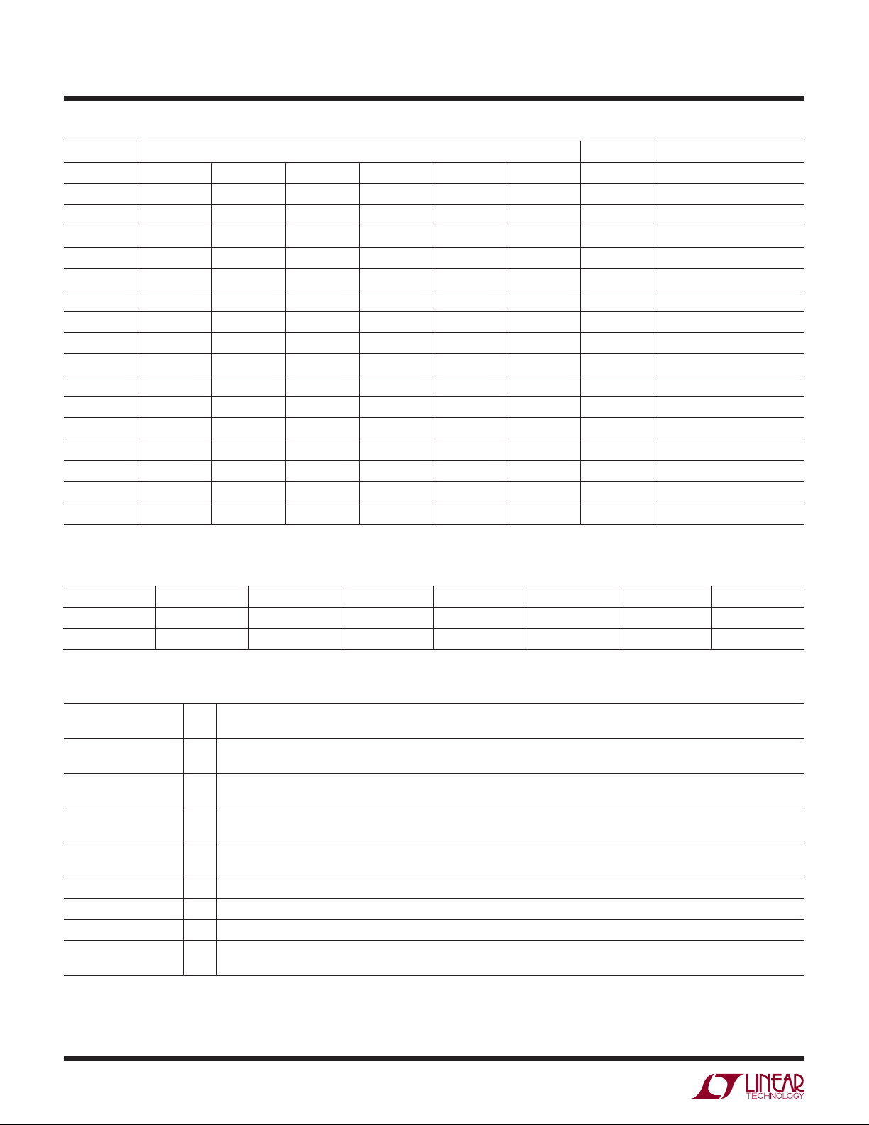
The LTC3207/LTC3207-1 has 16 data registers, each
with its own sub-address as shown in Table 2. The data
is loaded into the registers when the device receives a
2
Stop bit. This device is written using the standard I
C
protocol. A 7-bit slave address and write bit is followed
by the 8-bit sub-address byte and an 8-bit data byte. The
only difference between the LTC3207 and LTC3207-1 is
2
C address.
the I
The LTC3207/LTC3207-1 is a slave I2C device that only
can receive data.
DATA BYTES
REG0 (Tables 3 and 4) is used to fl ash the CAM LED with
the CAMHL bit and set the charge pump to Auto, force 1x,
force 1.5x, or force 2x modes. It is also used to prepare for
a Quick write, or set the gradation UP bit. REG1 through
REG12 set the intensity and mode for the twelve individual
ULEDs (Table 5). REG13 is divided into two sub-registers
as illustrated in Table 6. The lower four bits, D3 to D0, are
the CAML register which sets the CAM LED in torch mode.
The upper four bits, D7 to D4, are the CAMH register, which
sets the CAM LED when in fl ash mode. REG14 is used to
select ULED1 to ULED8 for ENU control, as shown in Table
7. REG15 is separated into three portions as illustrated
in Tables 8 and 9. D3 to D0 are used to select ULED9 to
ULED12 for ENU control. D5 and D4 are used to control
the gradation time, while D7 and D6 are used to select the
blinking on-time and period.
, LT, LTC and LTM are registered trademarks of Linear Technology Corporation.
All other trademarks are the property of their respective owners.
Table 1. Features of LTC3207/LTC3207-1
FEATURE BENEFITS
12 Separate 27.5mA Current Sources 12 Individually Controlled LEDs
Camera LED High Current Torch Mode
Blink Mode Blinks One of Four Blinking Patterns
GPO Mode I
Gradation Gradually Turns On and Off LEDs
External Enable (ENU) Controls LEDs with Single Input
Auto Switching Charge Pump Automatically Switches to 1x, 1.5x, or 2x Modes for Better Effi ciency
Forced Charge Pump Mode Can Be Programmed to Remain in 1x, 1.5x or 2x Mode
High Current Flash
2
C Controlled Open Drain Drivers
an108f
AN108-1
Application Note 108
Table 2. Sub-Address Byte
MSB LSB
76543210 Register
XXXX0000 REG0
XXXX0001 REG1
XXXX0010 REG2
XXXX0011 REG3
XXXX0100 REG4
XXXX0101 REG5
XXXX0110 REG6
XXXX0111 REG7
XXXX1000 REG8
XXXX1001 REG9
XXXX1010 REG10
XXXX1011 REG11
XXXX1100 REG12
XXXX1101 REG13
XXXX1110 REG14
XXXX1111 REG15
X = Don’t Care
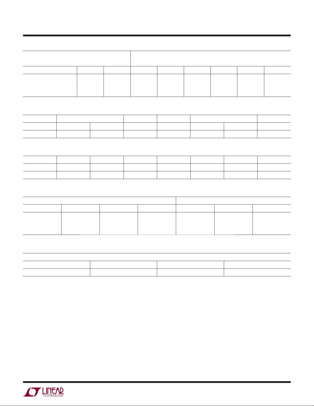
Table 3. REG0, Command Byte
MSB LSB
D7 D6 D5 D4 D3 D2 D1 D0
CAMHL Reserved Reserved Reserved Force2x Force1p5 Quickwrite UP
Table 4. Command Byte Bit Functions
UP 01Gradation Counts Down
Quickwrite 01Normal Write to Each Register
Force1p5 10Forces Charge Pump Into 1.5x Mode
Force2x 10Forces Charge Pump Into 2x Mode
Force1x
Reserved X
Reserved X
Reserved X
Camhilo 01External Control of CAM
Gradation Counts Up
Quick Write, REG1 Data is Written to All 12 Universal Registers
Enables Mode Logic to Control Mode Changes Based On Dropout Signal
Enables Mode Logic to Control Mode Changes Based On Dropout Signal
D2 (Force1p5x) = 1
D3 (Force2x) = 1
2
C Control of CAM
I
Forces Charge Pump Into 1x Mode
}
AN108-2
an108f
Application Note 108
Table 5. REG1 to REG12, Universal LED
BLINK/GRADATION/DROPOUT ENABLED LED CURRENT DATA
MSB LSB
Bits 76543210
Normal
Blink Enabled
Gradation Enabled
GPO Mode
Table 6. REG13, CAMH and CAML Registers
MSB HIGH BITS LSB MSB LOW BITS LSB
76543210
D3 D2 D1 D0 D3 D2 D1 D0
Table 7. REG14, Lower ENU Control Bits
MSB LSB
76543210
ULED8 ULED7 ULED6 ULED5 ULED4 ULED3 ULED2 ULED1
0
0
1
1
0
1
0
1
D5
D5
D5
D5
D4
D4
D4
D4
D3
D3
D3
D3
D2
D2
D2
D2
D1
D1
D1
D1
D0
D0
D0
D0
Table 8. REG15 MSB Nibble, Gradation and Blink Times
BLINK TIMES GRADATION TIMES
7 6 Blink Period 5 4 Gradation
0
0
1
1
0
1
0
1
0.625s
0.156s
0.625s
0.156s
Table 9. REG15 LSB Nibble, Upper ENU Control Bits
3210
ULED12 ULED11 ULED10 ULED9
1.25s
1.25s
2.5s
2.5s
ENU OUTPUT SELECTION
0
0
1
1
0
1
0
1
Disabled
0.24s
0.48s
0.96s
an108f
AN108-3

Application Note 108
DEVICE SET UP AND OPERATION
Although the power-on reset clears all the data registers,
it is good practice to write zeros to all the data registers
to make sure all data registers are reset after V
ers up. DV
holding DV
may also be used to reset the registers by
CC
low until V
CC
completes power up. The
BAT
BAT
pow-
Quick Write feature may also be used to clear the ULED
2
registers simultaneously with fewer I
To set one or more ULED(s) using the I
C writes.
2
C bus, write the
intensity setting to the desired ULED registers followed
by a Stop bit. The following example illustrates how to set
ULED1 and ULED2 to 5mA. Since the full-scale current
is 27.5mA, use the following formula to determine the
number of steps needed to acquire 5mA.
Steps = I
• StepsFullScale/IFullScale
LED
5mA • 63Steps/27.5mA = 11.45 Steps
The number of steps is rounded to 11 and converted to
the hexadecimal value 0BH. Setting the ULED register to
0BH will set the ULED to approximately 5mA.
Example 1: Setting ULED1 and ULED2 to 5mA
S 36H 01H 0BH ‘Set ULED1 to 5mA, No Stop bit’
charge pump to change modes (drop-out). For low speed
applications, the GPO current setting should be set greater
than the maximum current needed, however setting the
current greater than 10 times the maximum current may
increase the quiescent current by more than 10%.
Example 2: Set ULED1 and ULED2 to 1mA in
GPO mode
S 36H 01H C2H ‘Set ULED1 to 1mA in GPO mode’
S 36H 02H C2H P ‘Set ULED2 to GPO mode, Stop
bit loads data’
Blinking LEDs may be used to indicate voicemail messages, missed calls, low battery, or other messages. The
LTC3207/LTC3207-1 has a blinking feature that allows
the user to choose between one of four different blinking
2
rates. This feature reduces processor time and I
C traffi c.
To set a ULED to blink:
1) Set the blinking rate in REG15.
2) Set the ULED register with the desired intensity and the
blinking bit set, followed by a Stop bit.
The blink rate may be changed at any time by changing
the blink bits in register 15.
S 36H 02H 0BH P ‘Set ULED2 to 5mA, Stop bit
loads data’
In Example 1, the “S” designates the Start bit and 36H
designates the 7-bit slave address plus the Write bit to
form the 8-bit hexadecimal byte of 36 for the LTC3207.
For the LTC3207-1, substitute 34H in place of 36H for
the 7-bit slave address and Write bit. The second hexadecimal bytes, 01 and 02, are the sub-address bytes. The
third hexadecimal byte is the register data byte. The “P”
designates the Stop bit. The Stop bit was set after the last
write to load the ULED1 and ULED2 registers and set the
LEDs simultaneously. A Stop bit may be used after each
2
C write except where specifi ed when gradating. All of
I
the following examples will use the same format used in
Example 1.
The GPO mode may be used as an open drain output to
drive some other device. This is accomplished by allowing the ULED pin to be driven to 0V without causing the
Example 3: Setting ULED1 and ULED2 to blink at 5mA
with a 2.5s period and a 0.625s on-time:
S 36H 0FH 80H ‘Set blinking time to 0.625s on,
2.5s period’
S 36H 01H 4BH ‘Set ULED1 to blink at 5mA’
S 36H 02H 4BH P ‘Set ULED2 to blink, Stop bit
loads all data’
It is sometimes desirable to gradually turn on and off
2
LEDs or displays. Normally it uses a lot of I
C bus time to
gradually turn on and off LEDs smoothly. The LTC3207/
LTC3207-1 has a gradation feature that allows the user
2
to smoothly turn on and off LEDs with little I
tion. Gradation may be controlled with the I
2
the ENU pin only when the I
C bus is not controlling the
C interac-
2
C bus or by
device. To gradate a ULED from the off to on state via the
AN108-4
an108f

Application Note 108
I2C bus, the following procedure must be followed in order
to achieve the proper results.
1) Clear the Up bit in REG0 followed by a Stop bit.
2) Set the gradation time in REG15, without a Stop bit.
3) Set the ULED register with the gradation bit set and
without a Stop bit.
4) Set the Up bit in REG0 followed by a Stop bit.
The Stop bit loads the registers and starts the gradation
process. Never have the ULED gradation bit set without
the gradation timer enabled. This is an invalid state and
may cause undesirable results.
Example 4: Start gradating ULED1 and ULED2 from
0mA to 5mA at 0.48s ramp time:
S 36H 00H 00H P ‘Clear Up bit to prepare
gradation ramp’
S 36H 0FH 20H ‘Set Gradation time, No Stop bit’
S 36H 01H 8BH ‘Set ULED1 to gradate to 5mA,
No Stop bit’
The ULEDs may be set to gradate off from an on state.
To do this:
1) Clear the Up bit in REG0.
2) Set the ULED with the current intensity and the
gradation bit set without a Stop bit.
3) Enable the gradation timer followed by a Stop bit.
4) Set the ULED intensity to 0 with the gradation bit set.
Step 4 must be completed before the gradation ramp
completes or the ULEDs will fl icker at a low intensity. If
all ULEDs, charge pump, and camera LED are off, then
the part will go into shutdown.
Example 6: Start gradating ULED1 and ULED2 from
5mA to 0mA
NOTE: These steps must be completed within the gradation time.
S 36H 00H 00H P ‘Clear Up bit’
S 36H 01H 8BH ‘Set ULED1 with gradation bits,
No Stop bit’
S 36H 02H 8BH ‘Set ULED2 to gradate to 5mA
No Stop bit’
S 36H 00H 01H P ‘Set Up bit, Stop bit starts
gradation’
Prior to disabling the gradation timer in register 15 or
gradating up any other ULEDs, the gradation bits in the
ULED register must be cleared. This is accomplished by
writing an intensity value with the gradation bit cleared.
Example 5: Disabling gradation timer with ULED1 and
ULED2 at 5mA.
S 36H 01H 0BH ‘Set ULED1 to 5mA with
gradation bit low’
S 36H 02H 0BH ‘Set ULED2 to 5mA with
gradation bit low’
S 36H 0FH 00H P ‘Disable gradation timer, Stop bit
loads all data’
S 36H 02H 8BH ‘Set ULED2 with gradation bits,
No Stop bit’
S 36H 0FH 20H P ‘Set gradation timer, Stop bit
starts gradation’
S 36H 01H 80H ‘Set ULED1 & ULED2 registers
to 0 with gradation bit set’
S 36H 02H 80H P ‘Stop bit loads data’
The ULED gradation bit must be cleared before the
gradation timer in register 15 is disabled.
It may be desirable to continuously gradate a ULED up
and down. This may be achieved by fi rst initiating the
gradation as in Example 4 or Example 6. Once gradation
is initiated, set the ULED intensity and toggle the Up bit
followed by a Stop bit. To gradate down after gradating
up as illustrated in example 4:
1) Clear the Up bit followed by a Stop bit. This starts the
ULEDs gradating down.
2) Clear the ULED registers with the gradation bit set.
an108f
AN108-5

Application Note 108
Example 7: Continue gradating down after gradating
up as illustrated in Example 4
S 36H 00H 00H P ‘Clear Up bit, Stop bit starts
gradation ramp down’
S 36H 01H 80H ‘Set ULED1 register to 0 with
gradation bit set’
S 36H 02H 80H P ‘Set ULED2 to 0, Stop bit
loads data’
To gradate back up again:
1) Set the ULED intensity with the gradation bit set and
without a Stop bit.
2) Set the Up bit in REG0 followed by a Stop bit.
This starts the ULEDs gradating up.
Example 8: Continue gradating ULED1 and ULED2
back up to 5mA after gradating down
S 36H 01H 8BH ‘Set ULED1 to gradate to 5mA,
No Stop bit’
S 36H 02H 8BH ‘Set ULED2 to gradate to 5mA,
No Stop bit’
S 36H 00H 01H P ‘Set Up bit, Stop bit starts
gradation’
There may be times when all the ULEDs need to be changed
to the same value simultaneously. The LTC3207/LTC3207-1
has a “Quick Write” feature that allows all the ULED registers to be loaded at the same time. This is done by setting
the Quick Write bit in REG0 and then writing the desired
value in REG1. This feature may also be used to start all
the ULEDs blinking or gradating.
Example 9: Clearing all ULED registers using the
Quick Write feature
S 36H 00H 02H ‘Set the Quick Write bit’
S 36H 01H 00H P ‘Clear all ULEDs with Stop bit’
S 36H 00H 00H P ‘Clear Quick Write bit’
The Quick Write feature may also be used to start all the
ULEDs blinking or gradating. To gradate all ULEDs up
using the Quick Write feature:
1) Set the Quick Write bit and clear the Up bit in REG0
followed by a Stop bit.
2) Set REG1 gradation bit with the desired intensity without
a Stop bit.
3) Set the gradation time in REG15 without a Stop bit.
4) Clear the Quick Write bit and set the Up bit in REG0
followed by a Stop bit.
The Stop bit starts the gradation ramp.
Example 10: Start gradating all ULEDs up from 0mA to
5mA using the Quick Write feature
S 36H 00H 02H P ‘Set the Quick Write bit, Clear
the Up bit’
S 36H 01H 8BH ‘Set ULEDs to gradate to 5mA,
No Stop bit’
S 36H 0FH 20H ‘Set the gradation time,
No Stop bit’
S 36H 00H 01H P ‘Clear Quick Write bit, Set Up bit,
Gradation starts’
The Quick Write feature is especially useful when gradating down all ULEDs simultaneously. This feature may
reduce the number of I
to fi ve times. To gradate all ULEDs down using the Quick
Write feature:
1) Set the Quick Write bit and clear the Up bit in REG0.
2) Set REG1 gradation bit with the present intensity
setting without a Stop bit. This sets up all ULEDs to
gradate down.
3) Set the gradation time in REG15 followed by a Stop bit.
This starts all ULEDs gradating down.
4) Set REG1 gradation bit with 0mA intensity. This allows
the part to go into shutdown when gradation is
completed.
2
C writes from twenty six times
AN108-6
5) Clear the Quick Write bit in REG0.
This prepares the part for other operations.
an108f

Application Note 108
Example 11: Start gradating all ULEDs down from
5mA to 0mA using Quick Write
S 36H 00H 02H ‘Set Quick Write, Clear Up bit’
S 36H 01H 8BH ‘Set all ULEDs for gradation,
No Stop bit’
S 36H 0FH 20H P ‘Set gradation time, Stop bit
starts gradation’
S 36H 01H 80H P ‘Set all ULED registers to 0 with
gradation bit set’
S 36H 00H 00H ‘Clear Quick Write bit’
ENU Control
Many battery devices go into a standby or sleep mode when
not in use. It may be necessary to alert the user of events
while keeping the microprocessor in standby mode. The
ENU pin on the LTC3207/LTC3207-1 allows the user to
set ULEDs in normal, GPO, blinking, or gradation modes
2
without the use of the I
to be used when I
2
C may be used to drive other ULEDs as long as the
the I
C bus. The ENU pin is intended
2
C control is not preferred, however
gradation timer remains disabled. To control a ULED via
the ENU pin in normal, GPO, or blinking modes:
1) Set the ENU pin to the desired state, high if LEDs are
on or low if LEDs are off.
2) Set the ENU control bits and set the blinking time, if
required, in REG14 and/or REG15.
S 36H 01H 4BH ‘Set ULED1 to blink at 5mA’
S 36H 02H 4BH P ‘Set ULED2 to blink, Stop bit
loads data’
Set ENU pin to DV
to initiate ULED1 and ULED2
CC
blinking.
The ENU pin may also be used to control gradation, however it is important that all other ULEDs and the camera
LED remain off, and that the charge pump remains in
auto mode (not forced to any mode) to allow the part to
go into shutdown and to operate properly. This mode may
be initiated with the ULEDs in the on or off states, but care
must be taken not to turn on any other LEDs or change the
charge pump from auto mode once gradation with ENU
control is set. To gradate on with the ENU pin:
1) Make sure all ULEDs are off, the camera register is 0,
the charge pump is in auto mode, and the ENU pin is
set to 0V. The Quick Write feature may be used to clear
all ULEDs quickly.
2) Select the desired ULEDs for ENU control in REG14
and/or REG15.
3) Set the gradation time followed by a Stop bit.
4) Set the ULEDs intensity with the gradation bit set,
followed by a Stop bit.
The ULEDs are now set to gradate using ENU control. Set
the ENU pin to DV
to gradate up, and to 0V to gradate
CC
down.
3) Set the ULED intensity with the desired control bits
followed by a Stop bit.
Example 12: Setting ULED1 and ULED2 to blink at
0.625s on for a period of 2.5s with ENU control
Set ENU pin to 0V ‘Starting with ULEDs off’
S 36H 0EH 03H ‘Set ULED1 & ULED2 for ENU
control’
S 36H 0FH 80H ‘Set blinking time to 0.625s on,
2.5s period’
Information furnished by Linear Technology Corporation is believed to be accurate and reliable.
However, no responsibility is assumed for its use. Linear Technology Corporation makes no representation that the interconnection of its circuits as described herein will not infringe on existing patent rights.
Example 13: Gradate ULED1 and ULED2 to 5mA using
ENU control at 0.48s
Set ENU pin to 0V ‘Start with ULEDs off’
S 36H 00H 02H P ‘Set the Quick Write bit’
S 36H 01H 00H P ‘Clear all ULEDs’
S 36H 00H 00H ‘Clear command reg., charge
pump=Auto’
S 36H 0DH 00H ‘Clear CAM register’
an108f
AN108-7

Application Note 108
S 36H 0EH 03H ‘Set ULED1 and ULED2 for ENU
control’
S 36H 0FH 20H P ‘Set gradation time for 0.48s’
S 36H 01H 8BH ‘Set ULED1 to gradate to 5mA’
S 36H 02H 8BH P ‘Set ULED2 to gradate to 5mA’
Set ENU pin to DV
to gradate up, and to OV to
CC
gradate down.
Before any other ULEDs or camera LED are turned on, the
ENU with gradation must be disabled. To do this:
1) Set the ENU pin in the desired state to have ULEDs
on or off.
2) Clear the ENU control bits without a Stop bit.
3) Clear the gradation timer bits without a Stop bit.
4) Set the ULED registers to the desired intensity with
the gradation bit low followed by a Stop bit after the
last write.
Example 14: Disabling ENU and gradation control
while ULED1 and ULED2 are set to 5mA
Set ENU pin High ‘Gradate ULEDs to on state’
S 36H 0EH 00H ‘Relinquish ENU control’
S 36H 0FH 00H ‘Disable gradation timer,
No Stop bit’
high. To set ULEDs to gradate with ENU control from the
on state:
1) Make sure all ULEDs that are not going to be ENU
controlled are off, the camera LED is off, and the charge
pump is in auto mode.
2) Set the ULEDs to be controlled to the desired value
with the gradation bit clear.
3) Set the ENU pin to DV
CC
.
4) Set the gradation timer and the ENU control bits in
REG14 and/or REG15 followed by a Stop bit.
5) Wait for the gradation ramp to fi nish.
6) Set the ULED registers to the desired intensity with the
gradation bit set.
The ULEDs will now gradate down and up under ENU
control.
Example 15: Gradating ULED1 and ULED2 from 5mA
with ENU control
S 36H 01H 0BH ‘Set ULED1 and ULED2 to 5mA’
S 36H 02H 0BH P
Set ENU pin High
S 36H 0EH 03H ‘Set ENU control’
S 36H 0FH 20H P ‘Set gradation ramp up at 0.48s’
S 36H 01H 0BH ‘Clear ULED1 gradation bit, set
to 5mA, No Stop bit’
S 36H 02H 0BH P ‘Stop bit loads data
simultaneously’
Gradation with ENU may also be initiated with the ULEDs
to be controlled in the on state. To do this the gradation
ramp must fi rst be ramped up and the ENU pin must be
Linear Technology Corporation
AN108-8
1630 McCarthy Blvd., Milpitas, CA 95035-7417
(408) 432-1900 ● FAX: (408) 434-0507
●
www.linear.com
’Wait for gradation ramp to fi nish before setting ULED
gradation bits
S 36H 01H 8BH ‘Set ULED gradation bit and
intensity’
S 36H 02H 8BH P ‘Stop bit enables gradation with
ENU control’
an108f
LT 0707 • PRINTED IN USA
© LINEAR TECHNOLOGY CORPORATION 2007
 Loading...