

FEATURES
LTC3200/LTC3200-5
Low Noise, Regulated
Charge Pump DC/DC Converters
U
DESCRIPTIO
■
Low Noise Constant Frequency Operation
■
Output Current: 100mA
■
Available in 8-Pin MSOP (LTC3200) and Low
Profile (1mm) 6-Pin ThinSOTTM (LTC3200-5)
Packages
■
2MHz Switching Frequency
■
Fixed 5V ± 4% Output (LTC3200-5) or ADJ
■
VIN Range: 2.7V to 4.5V
■
Automatic Soft-Start Reduces Inrush Current
■
No Inductors
■
ICC <1µA in Shutdown
U
APPLICATIO S
■
White LED Backlighting
■
Li-Ion Battery Backup Supplies
■
Local 3V to 5V Conversion
■
Smart Card Readers
■
PCMCIA Local 5V Supplies
The LTC®3200/LTC3200-5 are low noise, constant frequency switched capacitor voltage doublers. They produce a regulated output voltage from a 2.7V to 4.5V input
with up to 100mA of output current. Low external parts
count (one flying capacitor and two small bypass capacitors at VIN and V
) make the LTC3200/LTC3200-5
OUT
ideally suited for small, battery-powered applications.
A new charge-pump architecture maintains constant
switching frequency to zero load and reduces both output
and input ripple. The LTC3200/LTC3200-5 have thermal
shutdown capability and can survive a continuous shortcircuit from V
to GND. Built-in soft-start circuitry
OUT
prevents excessive inrush current during start-up.
High switching frequency enables the use of small ceramic
capacitors. A low current shutdown feature disconnects
the load from VIN and reduces quiescent current to <1µA.
The LTC3200 is available in an 8-pin MSOP package and
the LTC3200-5 is available in a 6-pin ThinSOT.
, LTC and LT are registered trademarks of Linear Technology Corporation.
ThinSOT is a trademark of Linear Technology Corporation.
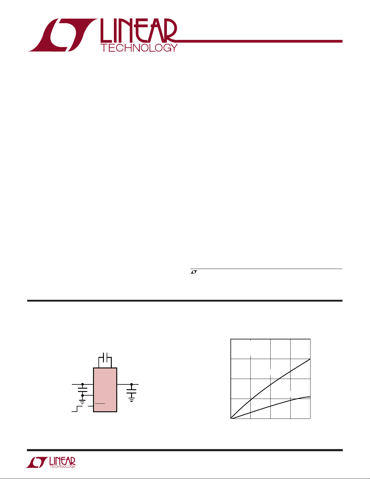
TYPICAL APPLICATIO
Regulated 5V Output from a 2.7V to 4.5V Input
1µF
4
+
–
C
C
ON
LTC3200-5
5
V
2
GND
3
SHDN
V
OUT
IN
V
2.7V TO 4.5V
IN
1µF
OFF
ALL CAPACITORS = MURATA GRM 39X5R105K6.3AJ
OR TAIYO YUDEN JMK107BJ105MA
U
Output Ripple Voltage vs Load Current
40
VIN = 3V
C
= 1µF
FLY
T
= 25°C
A
)
30
6
1
1µF
5V ±4%
V
OUT =
UP TO 40mA, VIN ≥ 2.7V
I
OUT
UP TO 100mA, VIN ≥ 3.1V
I
OUT
3200-5 TA01
P-P
20
OUTPUT RIPPLE (mV
10
0
0
25
OUTPUT CURRENT (mA)
C
= 1µF
OUT
C
= 2.2µF
OUT
50
75
100
3200 TA02
1
LTC3200/LTC3200-5
WW
W
ABSOLUTE AXI U RATI GS
U
(Note 1)
VIN to GND...................................................–0.3V to 6V
V
to GND .............................................– 0.3V to 5.5V
OUT
VFB, SHDN to GND........................ – 0.3V to (VIN + 0.3V)
I
(Note 2)....................................................... 150mA
OUT
UUW
PACKAGE/ORDER I FOR ATIO
ORDER PART
TOP VIEW
+
C
1
2
V
IN
–
3
C
4
PGND
MS8 PACKAGE
8-LEAD PLASTIC MSOP
T
= 150°C, θJA = 200°C/W
JMAX
Consult factory for parts specified with wider operating temperature ranges.
8
7
6
5
V
OUT
FB
SHDN
SGND
NUMBER
LTC3200EMS8
MS8 PART MARKING
LTNV
V
Short-Circuit Duration ............................. Indefinite
OUT
Operating Temperature Range (Note 3) .. –40°C to 85°C
Storage Temperature Range ................. –65°C to 150°C
Lead Temperature (Soldering, 10 sec).................. 300°C
ORDER PART
TOP VIEW
V
1
OUT
GND 2
SHDN 3
S6 PACKAGE
6-LEAD PLASTIC SOT-23
T
= 150°C, θJA = 230°C/W
JMAX
6 C
5 V
4 C
+
IN
–
NUMBER
LTC3200ES6-5
S6 PART MARKING
LTSH
ELECTRICAL CHARACTERISTICS
temperature range. Specifications are at TA = 25°C, VIN = 3.6V, C
SYMBOL PARAMETER CONDITIONS MIN TYP MAX UNITS
V
IN
V
OUT
I
CC
I
SHDN
V
FB
I
FB
V
R
η Efficiency (LTC3200-5) VIN = 3V, I
F
OSC
V
IH
V
IL
I
IH
I
IL
t
ON
R
OL
Note 1: Absolute Maximum Ratings are those values beyond which the life
of a device may be impaired.
Note 2: Based on long term current density limitations.
Input Voltage ● 2.7 4.5 V
Output Voltage 2.7V ≤ VIN ≤ 4.5V, I
Operating Supply Current I
Shutdown Current SHDN = 0V, V
FB Voltage (LTC3200) ● 1.217 1.268 1.319 V
FB Input Current (LTC3200) VFB = 1.4V ● –50 50 nA
Output Ripple (LTC3200-5) VIN = 3V, I
Switching Frequency 1 2 MHz
SHDN Input Threshold ● 1.3 V
SHDN Input Threshold ● 0.4 V
SHDN Input Current SHDN = V
SHDN Input Current SHDN = 0V ● –1 1 µA
V
Turn-On Time VIN = 3V, I
OUT
Open-Loop Output Resistance VIN = 3V, I
The ● denotes specifications which apply over the full operating
FLY
3.1V ≤ V
OUT
≤ 4.5V, I
IN
= 0mA, SHDN = V
OUT
OUT
IN
OUT
OUT
= 1µF, CIN = 1µF, C
≤ 40mA ● 4.8 5 5.2 V
OUT
≤ 100mA ● 4.8 5 5.2 V
OUT
IN
= 0V ● 1 µA
OUT
= 100mA 30 mV
= 50mA 80 %
= 0mA, 10% to 90% 0.8 ms
= 100mA, VFB = 0V (Note 4) 9.2 Ω
Note 3: The LTC3200E/LTC3200E-5 are guaranteed to meet performance
specifications from 0°C to 70°C. Specifications over the –40°C to 85°C
operating temperature range are assured by design, characterization and
correlation with statistical process controls.
Note 4: R
≡ (2 VIN – V
OL
= 1µF unless otherwise noted.
OUT
● 3.5 8 mA
● –1 1 µA
)/I
OUT
OUT
P-P
2
UW
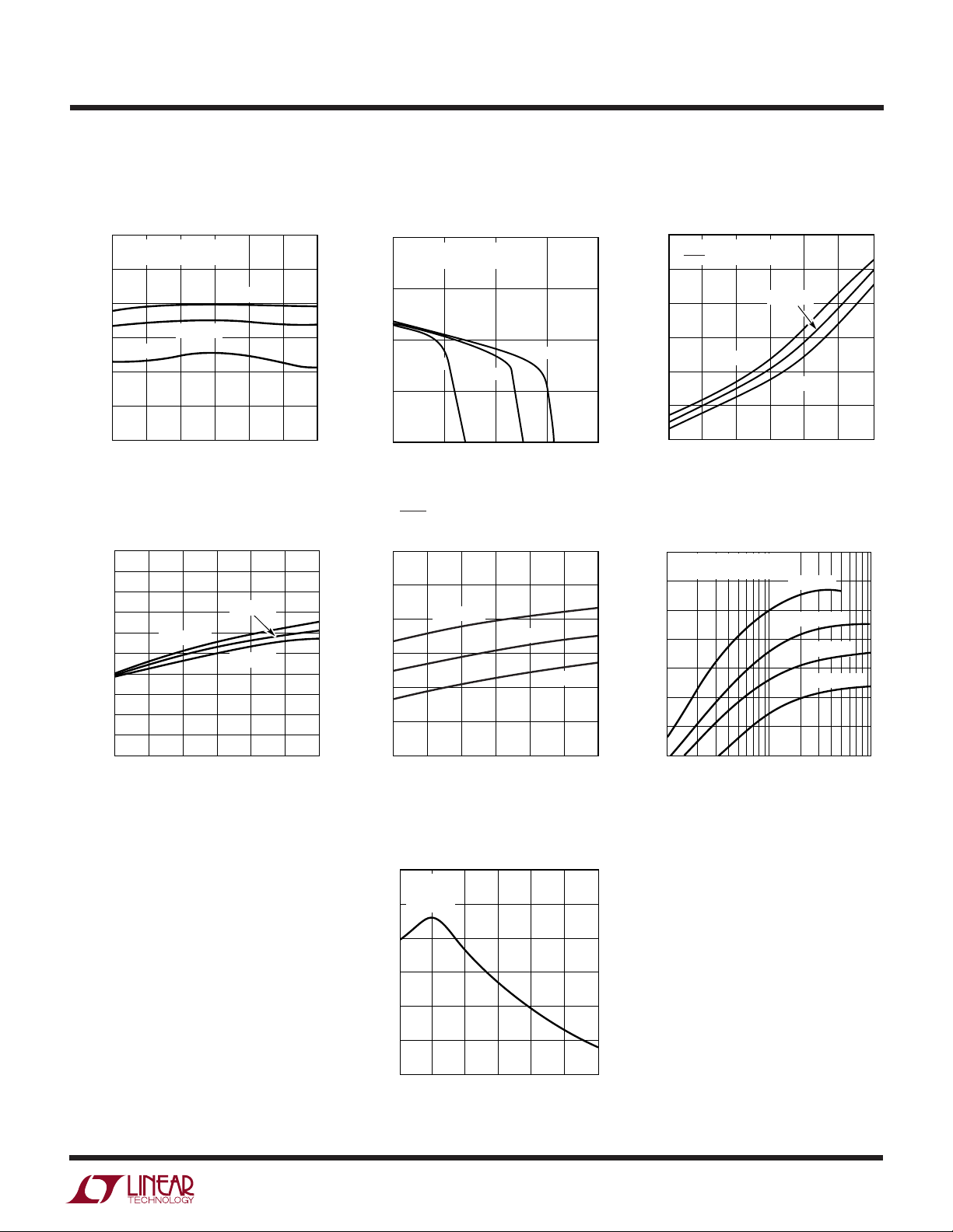
TYPICAL PERFOR A CE CHARACTERISTICS
Output Voltage vs Supply Voltage Output Voltage vs Load Current
5.15
CIN = C
I
5.10
5.05
5.00
4.95
OUTPUT VOLTAGE (V)
4.90
OUT
= 20mA
OUT
TA = –40°C
= C
= 1µF
FLY
TA = 25°C
TA = 85°C
5.2
CIN = C
T
5.1
5.0
VIN = 2.7V
OUTPUT VOLTAGE (V)
4.9
= 25°C
A
OUT
= C
= 1µF
FLY
VIN = 3V
VIN = 3.2V
LTC3200/LTC3200-5
(LTC3200-5)
No Load Supply Current vs Supply
Voltage
6
CIN = C
V
5
4
SUPPLY CURRENT (mA)
SHDN
OUT
= V
= C
FLY
IN
TA = 85°C
= 1µF
TA = 25°C
TA = –40°C
4.85
2.7
3.3 3.6 3.9
3.0
SUPPLY VOLTAGE (V)
Oscillator Frequency vs Supply
Voltage
3.0
2.8
2.6
2.4
2.2
2.0
1.8
1.6
1.4
OSCILLATOR FREQUENCY (MHz)
1.2
1.0
2.7 3.0 3.3 3.6 3.9
TA = –40°C
SUPPLY VOLTAGE (V)
TA = 25°C
TA = 85°C
4.2 4.5
3200 F01
3200 G04
4.8
0
V
50
Threshold Voltage vs
SHDN
100
LOAD CURRENT (mA)
150
200
3200 G02
Supply Voltage
1.1
1.0
0.9
0.8
0.7
THRESHOLD VOLTAGE (V)
0.6
4.54.2
0.5
TA = –40°C
TA = 25°C
2.7 3.0 3.3 3.6 3.9
SUPPLY VOLTAGE (V)
TA = 85°C
4.54.2
3200 G05
3
3.0 3.3 3.6 3.9
2.7
SUPPLY VOLTAGE (V)
Efficiency vs Load Current
100
CIN = C
T
90
80
70
60
EFFICIENCY (%)
50
40
30
1 10 100
= 25°C
A
OUT
= C
= 1µF
FLY
VIN = 2.7V
LOAD CURRENT (mA)
VIN = 3.2V
VIN = 3.7V
4.54.2
3200 G03
VIN = 4.5V
3200 G06
Short Circuit Current vs Supply
Voltage
250
C
= 1µF
FLY
= 25°C
T
A
= 0V
V
OUT
200
150
OUTPUT CURRENT (mA)
100
2.7
3.0 3.3 3.6 3.9
SUPPLY VOLTAGE (V)
4.54.2
3200 G07
3
LTC3200/LTC3200-5
I
L
10mA TO
90mA
50mA/DIV
V
OUT
(AC
COUPLED)
50mV/DIV
10µs/DIVV
IN
= 3.3V
C
OUT
= 1µF
32005 G10
UW
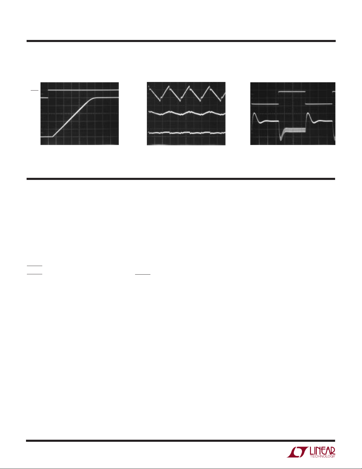
TYPICAL PERFOR A CE CHARACTERISTICS
(LTC3200-5) TA = 25°C
V
Soft-Start Ramp Output Ripple
OUT
V
(AC
OUT
V
SHDN
2V/DIV
V
OUT
1V/DIV
IN
= 3V
200µs/DIVV
32005 G08
COUPLED)
20mV/DIV
C
OUT
C
= 3.3µF
OUT
C
OUT
= 1µF
= 10µF
= 3.3V
IN
= 100mA
I
L
UUU
PIN FUNCTIONS
C+ (Pins 1/6): Flying Capacitor Positive Terminal.
VIN (Pins 2/5): Input Supply Voltage. VIN should be
bypassed with a 1µF to 4.7µF low ESR ceramic capacitor.
C– (Pins 3/4): Flying Capacitor Negative Terminal.
GND (Pins 4,5/2): Ground. Should be tied to a ground
plane for best performance.
LTC3200/LTC3200-5
Load Transient Response
200ns/DIVV
32005 G09
FB (Pin 7): (LTC3200 Only) Feedback Input Pin. An output
divider should be connected from V
to FB to program
OUT
the output voltage.
V
(Pins 8/1): Regulated Output Voltage. V
OUT
OUT
should
be bypassed with a 1µF to 4.7µF low ESR ceramic capaci-
tor as close as possible to the pin for best performance.
SHDN (Pins 6/3): Active Low Shutdown Input. A low on
SHDN disables the LTC3200/LTC3200-5. SHDN must not
be allowed to float.
4

W
SI PLIFIEDWBLOCK DIAGRA S
LTC3200/LTC3200-5
LTC3200
SOFT-START
AND
SWITCH CONTROL
V
8
OUT
FB
7
2MHz
OSCILLATOR
6
SHDN
–
+
CHARGE
PUMP
+
C
1
V
2
IN
4
5
PGND
SGND
–
C
3
3200 BD
LTC3200-5
SOFT-START
AND
SWITCH CONTROL
V
1
OUT
2MHz
–
OSCILLATOR
3
SHDN
+
CHARGE
PUMP
+
C
6
V
5
IN
–
C
4
2
GND
3200-5 BD
5

LTC3200/LTC3200-5
IC
V
ms
STARTUP OUT
OUT
= 2
1
U
OPERATIO
Operation (Refer to Simplified Block Diagrams)
The LTC3200/LTC3200-5 use a switched capacitor charge
pump to boost VIN to a regulated output voltage. Regulation is achieved by sensing the output voltage through an
internal resistor divider (LTC3200-5) and modulating the
charge pump output current based on the error signal. A
2-phase nonoverlapping clock activates the charge pump
switches. The flying capacitor is charged from VIN on the
first phase of the clock. On the second phase of the clock
it is stacked in series with VIN and connected to V
OUT
. This
sequence of charging and discharging the flying capacitor
continues at a free running frequency of 2MHz (typ).
In shutdown mode all circuitry is turned off and the
LTC3200/LTC3200-5 draw only leakage current from the
VIN supply. Furthermore, V
is disconnected from VIN.
OUT
The SHDN pin is a CMOS input with a threshold voltage of
approximately 0.8V. The LTC3200/LTC3200-5 is in shutdown when a logic low is applied to the SHDN pin. Since
the SHDN pin is a high impedance CMOS input it should
never be allowed to float. To ensure that its state is defined
it must always be driven with a valid logic level.
Short-Circuit/Thermal Protection
The LTC3200/LTC3200-5 have built-in short-circuit current
limiting as well as overtemperature protection. During
short-circuit conditions, they will automatically limit their
output current to approximately 225mA. At higher temperatures, or if the input voltage is high enough to cause excessive self heating on chip, thermal shutdown circuitry will
shut down the charge pump once the junction temperature
exceeds approximately 160°C. It will reenable the charge
pump once the junction temperature drops back to approximately 155°C. The LTC3200/LTC3200-5 will cycle in and
out of thermal shutdown indefinitely without latch-up or
damage until the short-circuit on V
is removed.
OUT
Shutdown Current
Since the output voltage can go above the input voltage,
special circuitry is required to control internal logic.
Detection logic will draw an input current of 5µA when the
LTC3200 is in shutdown. However, this current will be
eliminated when the output voltage (V
) is at 0V. To
OUT
ensure that V
LTC3200 a bleed resistor may be needed from V
is at 0V in shutdown on the adjustable
OUT
to GND.
OUT
Typically 10k to 100k is acceptable.
Soft-Start
The LTC3200/LTC3200-5 have built-in soft-start circuitry
to prevent excessive current flow at VIN during start-up.
The soft-start time is preprogrammed to approximately
1ms, so the start-up current will be primarily dependent
upon the output capacitor. The start-up input current can
be calculated with the expression:
For example, with a 2.2µF output capacitor the start-up
input current of an LTC3200-5 will be approximately
22mA. If the output capacitor is 10µF then the start-up
input current will be about 100mA.
Programming the LTC3200 Output Voltage (FB Pin)
While the LTC3200-5 version has an internal resistive
divider to program the output voltage, the programmable
LTC3200 may be set to an arbitrary voltage via an external
resistive divider. Since it employs a voltage doubling
charge pump, it is not possible to achieve output voltages
greater than twice the available input voltage. Figure 1
shows the required voltage divider connection.
The voltage divider ratio is given by the expression:
R
R
V
1
OUT
2 1 268
.
1=
–
V
Typical values for total voltage divider resistance can
range from several kΩs up to 1MΩ.
8
V
OUT
FB
PGND
SGND
Figure 1. Programming the Adjustable LTC3200
R1
7
R2
4
5
V
OUT
1.268V 1 +
C
OUT
32005 F01
R1
()
R2
6

OPERATIO
LTC3200/LTC3200-5
U
Maximum Available Output Current
For the adjustable LTC3200, the maximum available output current and voltage can be calculated from the effective open-loop output resistance, ROL, and effective output
voltage, 2V
.
IN(MIN)
R
OL
+
2V
IN
–
Figure 2. Equivalent Open-Loop Circuit
+
I
OUTVOUT
–
32005 F02
From Figure 2 the available current is given by:
VV
2–
=
IN OUT
R
OL
I
OUT
Typical ROL values as a function of temperature are shown
in Figure 3.
11
I
= 100mA
OUT
= 1µF
C
FLY
= 0V
V
FB
VIN, V
10
9
OUTPUT RESISTANCE (Ω)
8
–50
–25
Figure 3. Typical ROL vs Temperature
Capacitor Selection
OUT
VIN = 2.7V
VIN = 3.3V
02550
AMBIENT TEMPERATURE (°C)
75 100
32005 • F03
The style and value of capacitors used with the LTC3200/
LTC3200-5 determine several important parameters such
as regulator control loop stability, output ripple, charge
pump strength and minimum start-up time.
Tantalum and aluminum capacitors are not recommended
because of their high ESR.
The value of C
ripple for a given load current. Increasing the size of C
directly controls the amount of output
OUT
OUT
will reduce the output ripple at the expense of higher
minimum turn on time and higher start-up current. The
peak-to-peak output ripple is approximately given by the
expression:
I
V
RIPPLEP P
Where f
OSC
≅
−
is the LTC3200/LTC3200-5’s oscillator fre-
quency (typically 2MHz) and C
OUT
fC
2•
OSC OUT
is the output charge
OUT
storage capacitor.
Both the style and value of the output capacitor can signifi-
cantly affect the stability of the LTC3200/LTC3200-5. As
shown in the Block Diagrams, the LTC3200/LTC3200-5
use a linear control loop to adjust the strength of the charge
pump to match the current required at the output. The
error signal of this loop is stored directly on the output
charge storage capacitor. The charge storage capacitor
also serves to form the dominant pole for the control loop.
To prevent ringing or instability on the LTC3200-5 it is
important for the output capacitor to maintain at least 0.47µF
of capacitance over all conditions. On the adjustable
LTC3200 the output capacitor should be at least 0.47µF ×
5V/V
to account for the alternate gain factor.
OUT
Likewise excessive ESR on the output capacitor will tend
to degrade the loop stability of the LTC3200/LTC3200-5.
The closed loop output resistance of the LTC3200-5 is
designed to be 0.5Ω. For a 100mA load current change,
the output voltage will change by about 50mV. If the output
capacitor has 0.3Ω or more of ESR, the closed loop
frequency response will cease to roll off in a simple one
pole fashion and poor load transient response or instability could result. Ceramic capacitors typically have exceptional ESR performance and combined with a tight board
layout should yield very good stability and load transient
performance.
To reduce noise and ripple, it is recommended that low
ESR (<0.1Ω) ceramic capacitors be used for both C
and C
. These capacitors should be 0.47µF or greater.
OUT
IN
As the value of C
controls the amount of output
OUT
ripple, the value of CIN controls the amount of ripple
present at the input pin (VIN). The input current to the
7

LTC3200/LTC3200-5
U
OPERATIO
LTC3200/LTC3200-5 will be relatively constant while the
charge pump is on either the input charging phase or the
output charging phase but will drop to zero during the
clock nonoverlap times. Since the nonoverlap time is
small (~25ns), these missing “notches” will result in only
a small perturbation on the input power supply line. Note
that a higher ESR capacitor such as tantalum will have
higher input noise due to the input current change times
the ESR. Therefore ceramic capacitors are again recommended for their exceptional ESR performance.
Further input noise reduction can be achieved by powering
the LTC3200/LTC3200-5 through a very small series inductor as shown in Figure 4. A 10nH inductor will reject the
fast current notches, thereby presenting a nearly constant
current load to the input power supply. For economy the
10nH inductor can be fabricated on the PC board with
about 1cm (0.4") of PC board trace.
10nH
V
IN
0.22µF
Figure 4. 10nH Inductor Used for
Additional Input Noise Reduction
1µF
V
IN
LTC3200/
LTC3200-5
GND
32005 F02
Flying Capacitor Selection
Warning: A polarized capacitor such as tantalum or
aluminum should never be used for the flying capacitor
since its voltage can reverse upon start-up of the LTC3200/
LTC3200-5. Low ESR ceramic capacitors should always
be used for the flying capacitor.
The flying capacitor controls the strength of the charge
pump. In order to achieve the rated output current it is
necessary to have at least 0.68µF of capacitance for the
flying capacitor.
For very light load applications the flying capacitor may be
reduced to save space or cost. The theoretical minimum
output resistance of a voltage doubling charge pump is
given by:
–
2
VV
IN OUT
R
OL MIN
Where f
C
is the value of the flying capacitor. The charge pump
FLY
≡≅
()
is the switching frequency (2MHz typ) and
OSC
IfC
OUT OSC FLY
1
will typically be weaker than the theoretical limit due to
additional switch resistance, however for very light load
applications the above expression can be used as a guideline in determining a starting capacitor value.
Ceramic Capacitors
Ceramic capacitors of different materials lose their capacitance with higher temperature and voltage at different
rates. For example, a capacitor made of X5R or X7R
material will retain most of its capacitance from – 40°C to
85°C whereas a Z5U or Y5V style capacitor will lose
considerable capacitance over that range. Z5U and Y5V
capacitors may also have a very poor voltage coefficient
causing them to lose 60% or more of their capacitance
when the rated voltage
is applied. Therefore, when comparing different capacitors it is often more appropriate to
compare the amount of achievable capacitance for a given
case size rather than discussing the specified capacitance
value. For example, over rated voltage and temperature
conditions, a 1µF, 10V, Y5V ceramic capacitor in an 0603
case may not provide any more capacitance than a
0.22µF, 10V, X7R available in the same 0603 case. In fact
for most LTC3200/LTC3200-5 applications these capacitors can be considered roughly equivalent . The capacitor
manufacturer’s data sheet should be consulted to determine what value of capacitor is needed to ensure the
desired capacitance at all temperatures and voltages.
Below is a list of ceramic capacitor manufacturers and
how to contact them:
AVX www.avxcorp.com
Kemet www.kemet.com
Murata www.murata.com
Taiyo Yuden www.t-yuden.com
Vishay www.vishay.com
8

OPERATIO
LTC3200/LTC3200-5
U
Power Efficiency
The power efficiency (η) of the LTC3200/LTC3200-5 is
similar to that of a linear regulator with an effective input
voltage of twice the actual input voltage. This occurs
because the input current for a voltage doubling charge
pump is approximately twice the output current. In an ideal
regulating voltage doubler the power efficiency would be
given by:
•
P
OUT
η≡ = =
P
VI
OUT OUT
VIVV
IN
IN OUT
•2 2
OUT
IN
At moderate to high output power the switching losses
and quiescent current of the LTC3200/LTC3200-5 are
negligible and the expression above is valid. For example
with VIN = 3V, I
= 50mA and V
OUT
regulating to 5V the
OUT
measured efficiency is 80% which is in close agreement
with the theoretical 83.3% calculation.
Operation at VIN > 5V
LTC3200/LTC3200-5 will continue to operate with input
voltages somewhat above 5V. However, because of its
constant frequency nature, some charge due to internal
switching will be coupled to V
causing a slight upward
OUT
movement of the output voltage at very light loads. To
avoid an output overvoltage problem with high VIN, a
moderate standing load current of 1mA will help the
LTC3200/LTC3200-5 maintain exceptional line regulation. This can be achieved with a 5k resistor from V
OUT
to
GND.
Layout Considerations
Due to its high switching frequency and the high transient
currents produced by the LTC3200/LTC3200-5, careful
board layout is necessary. A true ground plane and short
connections to all capacitors will improve performance and
ensure proper regulation under all conditions. Figure 5
shows an example layout for the LTC3200-5.
Thermal Management
For higher input voltages and maximum output current
there can be substantial power dissipation in the LTC3200/
LTC3200-5. If the junction temperature increases above
approximately 160°C the thermal shutdown circuitry will
automatically deactivate the output. To reduce the
maximum junction temperature, a good thermal connection to the PC board is recommended. Connecting the
GND pin (Pins 4/5 for LTC3200, Pin 2 for LTC3200-5) to
a ground plane, and maintaining a solid ground plane
under the device on two layers of the PC board can reduce
the thermal resistance of the package and PC board
considerably.
Derating Power at Higher Temperatures
To prevent an overtemperature condition in high power
applications Figure 6 should be used to determine the
maximum combination of ambient temperature and power
dissipation.
1.2
1.0
θJA = 175°C/W
= 160°C
T
J
V
V
OUT
GND
SHDN
IN
1µF
LTC3200-5
Figure 5. Recommended Layout
1µF 1µF
32005 F03
0.8
0.6
0.4
POWER DISSIPATION (W)
0.2
0
–50
Figure 6. Maximum Power Dissipation
vs Ambient Temperature
02550
–25
AMBIENT TEMPERATURE (°C)
75 100
32005 • F06
9

LTC3200/LTC3200-5
U
OPERATIO
The power dissipated in the LTC3200/LTC3200-5 should
always fall under the line shown for a given ambient
temperature. The power dissipated in the LTC3200/
LTC3200-5 is given by the expression:
PD ≡ (2VIN – V
OUT)IOUT
This derating curve assumes a maximum thermal
resistance, θJA, of 175°C/W for both the 6 pin ThinSOT
U
PACKAGE DESCRIPTIO
MS8 Package
8-Lead Plastic MSOP
(LTC DWG # 05-08-1660)
0.043
(1.10)
MAX
0.007
(0.18)
0.021 ± 0.006
(0.53 ± 0.015)
* DIMENSION DOES NOT INCLUDE MOLD FLASH, PROTRUSIONS OR GATE BURRS. MOLD FLASH,
PROTRUSIONS OR GATE BURRS SHALL NOT EXCEED 0.006" (0.152mm) PER SIDE
** DIMENSION DOES NOT INCLUDE INTERLEAD FLASH OR PROTRUSIONS.
INTERLEAD FLASH OR PROTRUSIONS SHALL NOT EXCEED 0.006" (0.152mm) PER SIDE
0° – 6° TYP
SEATING
PLANE
0.009 – 0.015
(0.22 – 0.38)
0.0256
(0.65)
BSC
LTC3200-5 and the 8 pin MSOP adjustable LTC3200
which can be achieved from a printed circuit board layout
with a solid ground plane and a good connection to the
ground pins of the LTC3200/LTC3200-5. Operation outside of this curve will cause the junction temperature to
exceed 160°C which may trigger the thermal shutdown
circuitry.
0.034
(0.86)
REF
0.005 ± 0.002
(0.13 ± 0.05)
0.118 ± 0.004*
(3.00 ± 0.102)
0.193 ± 0.006
(4.90 ± 0.15)
8
7
12
6
5
0.118 ± 0.004**
4
3
(3.00 ± 0.102)
MSOP (MS8) 1100
10

PACKAGE DESCRIPTIO
U
S6 Package
6-Lead Plastic ThinSOT-23
(LTC DWG # 05-08-1634)
LTC3200/LTC3200-5
2.80 – 3.10
(.110 – .118)
(NOTE 3)
SOT-23
(Original)
.90 – 1.45
A
(.035 – .057)
.00 – 0.15
A1
(.00 – .006)
.90 – 1.30
A2
(.035 – .051)
.35 – .55
L
(.014 – .021)
.20
(.008)
DATUM ‘A’
L
NOTE:
1. CONTROLLING DIMENSION: MILLIMETERS
2. DIMENSIONS ARE IN
3. DRAWING NOT TO SCALE
4. DIMENSIONS ARE INCLUSIVE OF PLATING
5. DIMENSIONS ARE EXCLUSIVE OF MOLD FLASH AND METAL BURR
6. MOLD FLASH SHALL NOT EXCEED .254mm
7. PACKAGE EIAJ REFERENCE IS:
SC-74A (EIAJ) FOR ORIGINAL
JEDEL MO-193 FOR THIN
SOT-23
(ThinSOT)
1.00 MAX
(.039 MAX)
.01 – .10
(.0004 – .004)
.80 – .90
(.031 – .035)
.30 – .50 REF
(.012 – .019 REF)
MILLIMETERS
(INCHES)
2.60 – 3.00
(.102 – .118)
(.004 – .008)
.09 – .20
(NOTE 2)
1.50 – 1.75
(.059 – .069)
(NOTE 3)
A
PIN ONE ID
.95
(.037)
REF
A2
1.90
(.074)
REF
.25 – .50
(.010 – .020)
(6PLCS, NOTE 2)
A1
S6 SOT-23 0401
Information furnished by Linear Technology Corporation is believed to be accurate and reliable.
However, no responsibility is assumed for its use. Linear Technology Corporation makes no representation that the interconnection of its circuits as described herein will not infringe on existing patent rights.
11

LTC3200/LTC3200-5
U
TYPICAL APPLICATIO S
3V TO 4.4V
Li-Ion
BATTERY
(APPLY PWM WAVEFORM FOR
ADJUSTABLE BRIGHTNESS CONTROL)
3V TO 4.4V
Li-Ion
BATTERY
ON
OFF
(APPLY PWM WAVEFORM FOR
ADJUSTABLE BRIGHTNESS CONTROL)
1µF
ON OFF
Lithium-Ion Battery to 5V White or Blue LED Driver
1µF
White or Blue LED Driver with LED Current Control
1µF
13
+
–
C
C
2
V
IN
LTC3200
6
SHDN
V
SHDN
1µF
46
–
C
5
V
IN
LTC3200-5
3
SHDN
V
SHDN
V
OUT
SGND
PGND
C
V
OUT
GND
8
1µF
7
FB
5
4
t
+
1
2
t
1µF
82Ω
100Ω
UP TO 6 LEDS
82Ω
82Ω 82Ω 82Ω 82Ω
DRIVE UP TO 5 LEDS
100Ω 100Ω
32005 TA04
100Ω 100Ω
3200-5 TA03
USB Port to Regulated 5V Power Supply
1µF
46
5
3
1µF 1µF
LTC3200-5
1
V
OUT
5V ±4%
50mA
2
32005 TA05
RELATED PARTS
PART NUMBER DESCRIPTION COMMENTS
LTC1682/-3.3/-5 Doubler Charge Pumps with Low Noise LDO MS8 and SO-8 Packages , I
LTC1751/-3.3/-5 Doubler Charge Pumps V
= 5V at 100mA; V
OUT
LTC1754-3.3/-5 Doubler Charge Pumps with Shutdown ThinSOT Package; IQ = 13µA; I
LTC1928-5 Doubler Charge Pump with Low Noise LDO ThinSOT Output Noise = 60µV
Linear Technology Corporation
12
1630 McCarthy Blvd., Milpitas, CA 95035-7417
(408) 432-1900 ● FAX: (408) 434-0507
●
www.linear-tech.com
OUT
= 3.3V at 80mA; ADJ; MSOP Packages
OUT
= 80mA, Output Noise = 60µV
= 50mA
OUT
; V
RMS
= 5V; VIN = 2.7V to 4V
OUT
32005f LT/TP 0501 2K • PRINTED IN USA
LINEAR TECHNOLOGY CORPORATION 2000
RMS
 Loading...