

LTC3125
1.2A Synchronous Step-Up
DC/DC Converter with
Input Current Limit
FEATURES
n
Programmable Average Input Current Limit
n
5% Input Current Accuracy
n
200mA to 1000mA Program Range
n
VIN: 1.8V to 5.5V, V
n
Supports High Current GSM/GPRS Load Burst
n
VIN > V
n
1.6MHz Fixed Frequency Operation
n
Internal Current Sense Resistor
n
1.2A Peak Current Limit
n
Up to 93% Effi ciency
n
Output Disconnect in Shutdown
n
Soft-Start
n
Low Quiescent Current Burst Mode® Operation (15µA)
n
Available in 2mm × 3mm × 0.75mm DFN Package
Operation
OUT
: 2V to 5.25V
OUT
APPLICATIONS
n
GSM/GPRS PCMCIA/CompactFlash PC Card Modems
n
Wireless Emergency Locators
n
Portable Radios
n
Supercap Chargers
DESCRIPTION
The LTC®3125 is a high effi ciency, synchronous step-up
DC/DC converter with an accurate programmable average
input current limit. The ±5% accurate average input current
is resistor programmable and suitable for a wide variety of
applications. In mobile computing, GSM and GPRS cards
demand high current pulses well beyond the capability
of the PC Card and CompactFlash slots. The LTC3125 in
concert with a reservoir capacitor, keeps the slot power
safely within its capabilities providing a high performance
and simple solution.
Synchronous rectifi cation produces high effi ciency while
the 1.6MHz switching frequency minimizes the solution
footprint. The current mode PWM design is internally compensated. Output disconnect allows the load to discharge in
shutdown, while also providing inrush current limiting.
Other features include a <1µA shutdown current, shortcircuit and thermal overload protection. The LTC3125 is offered in a low profi le 0.75mm × 2mm × 3mm package.
L, LT, LTC, LTM and Burst Mode are registered trademarks of Linear Technology Corporation.
All other trademarks are the property of their respective owners.
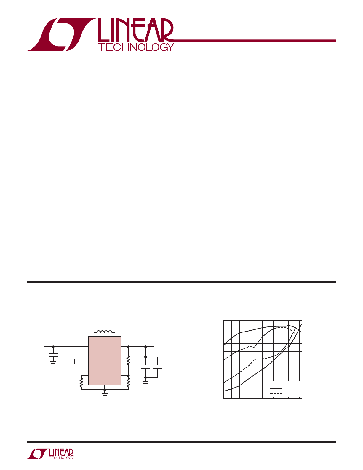
TYPICAL APPLICATION
PCMCIA/CompactFlash (3.3V/500mA Max),
4V GSM Pulsed Load
2.2µH
LTC3125
GND
SW
V
OUT
FB
V
3.3V
500mA
IN
10µF
CER
OFF ON
44.2k
CS
V
IN
SHDN
PROG
1.24M
536k
V
OUT
4V
2A PULSED LOAD
2200µF
s2
TANT
3125 TA01a
Effi ciency vs Load Current
100
90
80
70
60
50
40
EFFICIENCY (%)
30
20
10
0
0.001
V
= 4V
OUT
= 3.3V
V
IN
= 2.4V
V
IN
0.01 0.1 1
LOAD CURRENT (A)
3125 TA01b
1
POWER LOSS (W)
0.1
0.01
0.001
3125f
1
LTC3125
PIN CONFIGURATION ABSOLUTE MAXIMUM RATINGS
(Note 1)
VIN, V
Voltage ......................................... –0.3V to 6V
OUT
SW Voltage .................................................. –0.3V to 6V
SW Voltage < 100ns .................................... –0.3V to 7V
All Other Pins ............................................... –0.3V to 6V
Operating Temperature Range
(Notes 2, 5) .............................................. –40°C to 85°C
Junction Temperature ........................................... 125°C
Storage Temperature Range ................... –65°C to 125°C
GND
FB
PROG
V
IN
8-LEAD (2mm s 3mm) PLASTIC DFN
T
EXPOSED PAD (PIN 9) IS GND, MUST BE SOLDERED TO PCB
JMAX
TOP VIEW
1
2
3
4
= 125°C, θJA = 64°C/W (NOTE 6)
9
DCB PACKAGE
8
7
6
5
SW
V
OUT
SHDN
CS
ORDER INFORMATION
LEAD FREE FINISH TAPE AND REEL PART MARKING PACKAGE DESCRIPTION TEMPERATURE RANGE
LTC3125EDCB#PBF LTC3125EDCB#TRPBF LDGY
Consult LTC Marketing for parts specifi ed with wider operating temperature ranges.
Consult LTC Marketing for information on non-standard lead based fi nish parts.
For more information on lead free part marking, go to: http://www.linear.com/leadfree/
For more information on tape and reel specifi cations, go to: http://www.linear.com/tapeandreel/
8-Lead (2mm × 3mm) Plastic DFN
–40°C to 85°C
ELECTRICAL CHARACTERISTICS
The l denotes the specifi cations which apply over the full operating
temperature range, otherwise specifi cations are at TA = 25°C. VIN = 3.3V, V
PARAMETER CONDITIONS MIN TYP MAX UNITS
Input Voltage Range 1.8 5.5 V
Minimum Start-Up Voltage
Output Voltage Adjust Range
Feedback Voltage
Feedback Input Current 150 nA
Quiescent Current—Shutdown V
Quiescent Current —Active Measured on V
Quiescent Current—Burst Measured on V
N-Channel MOSFET Switch Leakage V
P-Channel MOSFET Switch Leakage V
N-Channel MOSFET Switch On-Resistance V
P-Channel MOSFET Switch On-Resistance V
N-Channel MOSFET Current Limit
Current Limit Delay to Output (Note 3) 60 ns
Average Input Current Limit R
= 0V, Not Including Switch Leakage, V
SHDN
, Nonswitching 300 500 µA
OUT
, FB = 1.230V 15 25 µA
OUT
= 5V, VIN = 5V 0.1 10 µA
SW
= 5V, V
SW
= 3.3V 0.125
OUT
= 3.3V 0.200
OUT
PROG
R
PROG
= 0V, VIN = 5V 0.1 20 µA
OUT
= 44.2k
= 44.2k, –40°C to 85°C
= 4.5V unless otherwise noted.
OUT
l
l
l
1.176 1.200 1.229 V
= 0V 0.01 1 µA
OUT
l
1.2 1.8 A
475
l
465
1.6 1.8 V
2 5.25 V
500
500
525
535
mA
mA
2
3125f
LTC3125
ELECTRICAL CHARACTERISTICS
The l denotes the specifi cations which apply over the full operating
temperature range, otherwise specifi cations are at T
PARAMETER CONDITIONS MIN TYP MAX UNITS
PROG Current Gain (Note 3) 22.1 k-A/A
Maximum Duty Cycle V
Minimum Duty Cycle V
Frequency
SHDN Input High 1V
SHDN Input Low 0.35 V
SHDN Input Current V
FB
FB
SHDN
= 25°C. VIN = 3.3V, V
A
= 1.15V
= 1.3V
= 4.5V unless otherwise noted.
OUT
l
l
l
85 92 %
0%
1.3 1.6 1.9 MHz
= 1.2V 0.3 1 µA
Note 1: Stresses beyond those listed under Absolute Maximum Ratings
may cause permanent damage to the device. Exposure to any Absolute
Maximum Rating condition for extended periods may affect device
reliability and lifetime.
Note 2: The LTC3125 is guaranteed to meet performance specifi cations
from 0°C to 85°C. Specifi cations over –40°C to 85°C operating
temperature range are assured by design, characterization and correlation
with statistical process controls.
Note 3: Specifi cation is guaranteed by design and not 100% tested in
Note 4: Current measurements are made when the output is not switching.
Note 5: This IC includes overtemperature protection that is intended
to protect the device during momentary overload conditions. Junction
temperature will exceed 125°C when overtemperature protection is active.
Continuous operation above the specifi ed maximum operating junction
temperature may result in device degradation or failure.
Note 6: Failure to solder the exposed backside of the package to the PC
board ground plane will result in a thermal resistance much higher than
60°C/W.
production.
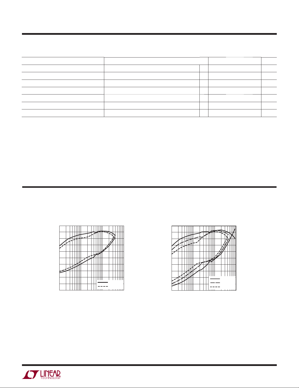
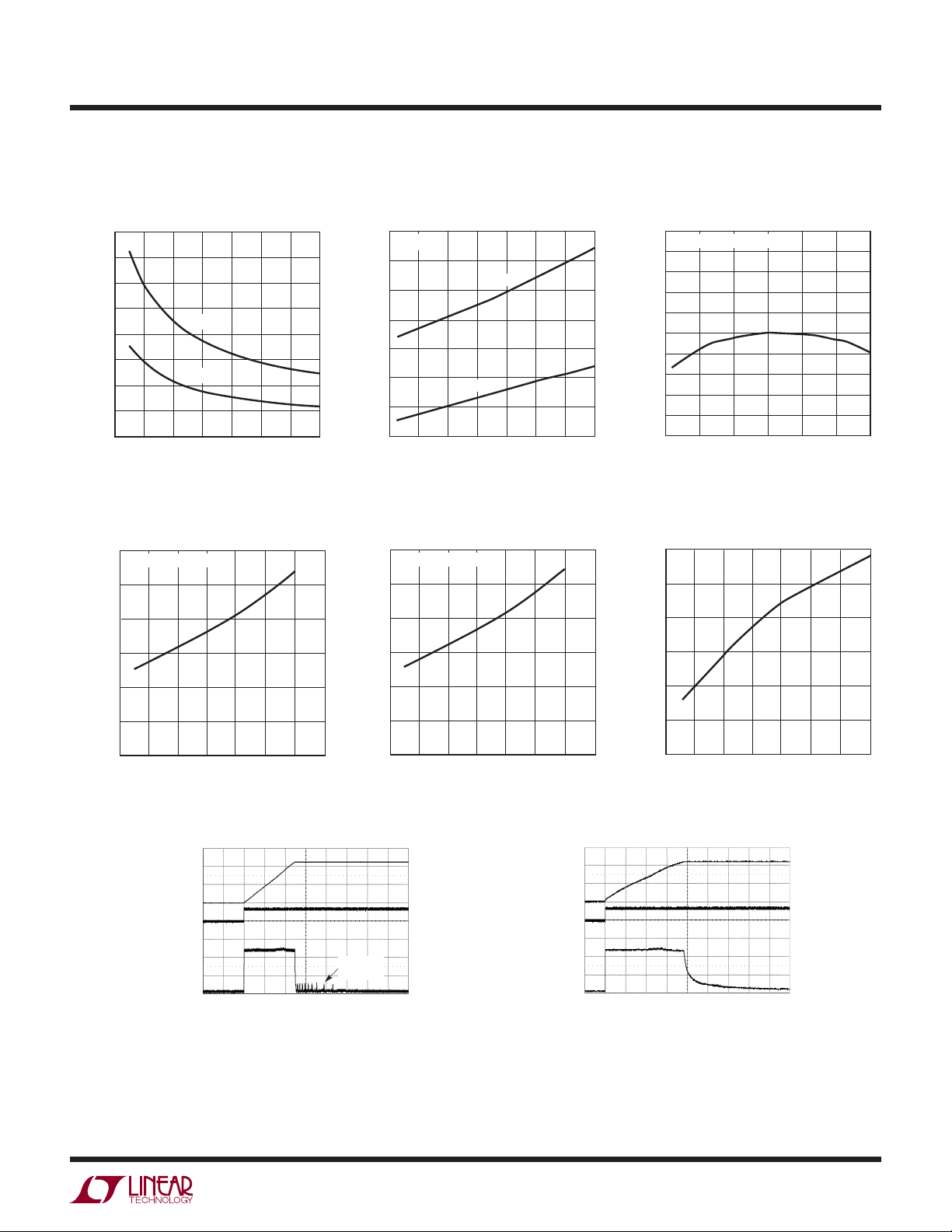
TYPICAL PERFORMANCE CHARACTERISTICS
Effi ciency vs Load Current,
V
= 2.5V
OUT
100
90
80
70
60
50
40
EFFICIENCY (%)
30
20
10
0
0.001
VIN = 2.1V
V
IN
0.01 0.1 1
LOAD CURRENT (A)
= 1.8V
3125 G01
1
0.1
POWER LOSS (W)
0.01
0.001
0.0001
100
90
80
70
60
50
40
EFFICIENCY (%)
30
20
10
0
0.001
(TA = 25°C unless otherwise noted)
Effi ciency vs Load Current,
V
= 3.3V
OUT
VIN = 2.8V
= 2.4V
V
IN
= 2V
V
IN
0.01 0.1 1
LOAD CURRENT (A)
3125 G02
1
POWER LOSS (W)
0.1
0.01
0.001
3125f
3
LTC3125
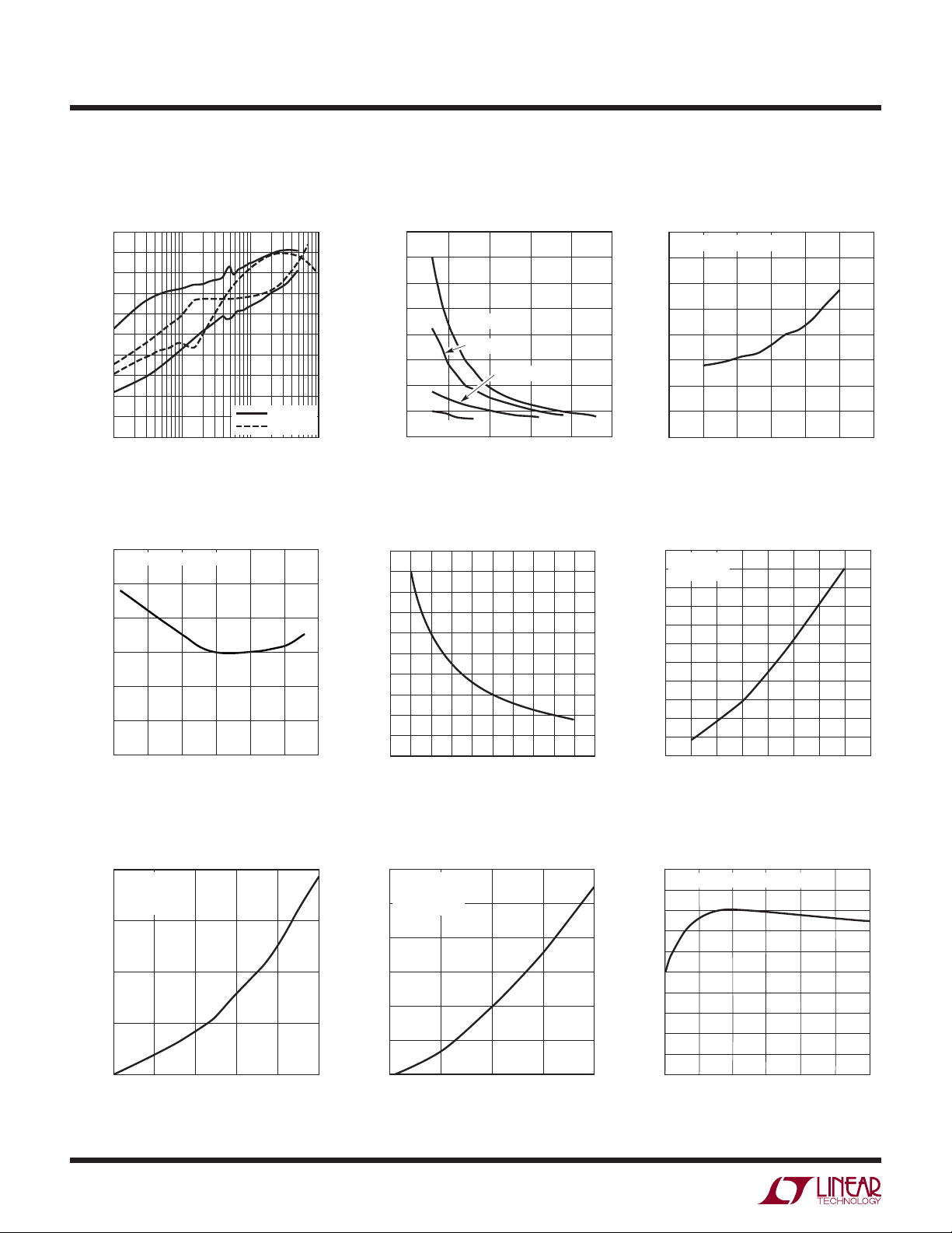
TYPICAL PERFORMANCE CHARACTERISTICS
Effi ciency vs Load Current,
V
= 5V
OUT
100
90
80
70
60
50
40
EFFICIENCY (%)
30
20
10
0
0.001
0.01 0.1 1
LOAD CURRENT (A)
VIN = 4V
V
Average Input Current Limit vs
Temperature
1.50
NORMALIZED TO 25°C
1.00
0.50
0
–0.50
–1.00
AVERAGE INPUT CURRENT LIMIT CHANGE (%)
–1.50
–50
02550
–25
TEMPERATURE (°C)
= 3.3V
IN
3125 G03
75 100
3125 G06
1
POWER LOSS (W)
0.1
0.01
0.001
No-Load Input Current vs V
4.0
3.5
3.0
2.5
2.0
(mA)
IN
I
1.5
1.0
0.5
0
1.5
V
= 4V
OUT
V
= 3.8V
OUT
V
= 3.3V
OUT
V
= 2.5V
OUT
2 2.5 3.5
VIN (V)
Average Input Current vs R
1.25
1.00
0.75
0.50
0.25
AVERAGE INPUT CURRENT LIMIT (A)
0
10 20 30 40 50 70 80 90 100
60 110
R
(k)
PROG
3
(TA = 25°C unless otherwise noted)
IN
4
3125 G04
PROG
3125 G07
Average Input Current Limit vs V
2.0
NORMALIZED TO 25°C
1.5
1.0
0.5
0
–0.5
–1.0
–1.5
AVERAGE INPUT CURRENT LIMIT CHANGE (%)
–2.0
2.0 2.5 3.5
1.5
Peak Current Limit vs V
2.55
V
= 3.8V
OUT
2.50
2.45
2.40
2.35
2.30
2.25
2.20
INPUT CURRENT (A)
2.15
2.10
2.05
2.00
1.5
R
PROG
= 0
2 2.5
3
3.0
VIN (V)
3.5
VIN (V)
IN
4.5
4.0
3125 G05
IN
4
4.5
5
3125 G08
5.5
Burst Mode Threshold Current
vs V
IN
50
V
= 3.3V
OUT
= 1500µF
C
OUT
L = 2.2µH
40
30
LOAD CURRENT (mA)
20
10
1.8
2.0
2.2
VIN (V)
4
2.4
2.6
3125 G09
2.8
Burst Mode Threshold Current
vs V
IN
50
V
= 2.5V
OUT
= 1500µF
C
OUT
45
L = 2.2µH
40
35
30
LOAD CURRENT (mA)
25
20
1.8
1.9 2.0 2.1 2.2
VIN (V)
3125 G10
Oscillator Frequency vs V
2
NORMALIZED TO V
1
0
–1
–2
–3
–4
–5
FREQUENCY CHANGE (%)
–6
–7
–8
2.5
2.0
3.0
OUT
V
OUT
3.5
= 3.3V
(V)
4.0
OUT
4.5
5.0
3125 G11
3125f
LTC3125
TYPICAL PERFORMANCE CHARACTERISTICS
R
R
vs V
DS(ON)
0.450
0.400
0.350
0.300
0.250
RDS(ON) ()
0.200
0.150
0.100
0.050
2 2.5 3.5
1.5
Feedback vs Temperature
0.50
NORMALIZED TO 25°C
0.25
OUT
PMOS
NMOS
V
3
OUT
(V)
4 4.5 5
3125 G12
240
220
200
180
(m)
160
DS(ON)
R
140
120
100
0.50
0.25
–50
vs Temperature
DS(ON)
V
= 4V
OUT
PMOS
NMOS
30 70 90
–30 –10
Current Sense Voltage (V
10 50
TEMPERATURE (°C)
RPROG
vs Temperature Burst Mode Current vs V
NORMALIZED TO 25°C
(TA = 25°C unless otherwise noted)
Oscillator Frequency
vs Temperature
10
NORMALIZED TO 25°C
8
6
4
2
0
–2
–4
FREQUENCY CHANGE (%)
–6
–8
–10
–50
–25
3125 G13
25 50
0
TEMPERATURE (°C)
)
16.0
15.5
OUT
75
100
3125 G14
0
(%)
FB
–0.25
–0.50
CHANGE IN V
–0.75
–1.00
–50
–30 –10
2V/DIV
SHDN
5V/DIV
INPUT
CURRENT
200mA/DIV
30 70 90
10 50
TEMPERATURE (°C)
V
and IIN During Soft-Start
OUT
V
OUT
= 3.3V
IN
= 4.5V
V
OUT
= 4.4mF
C
OUT
L = 2.7µH
0
(%)
FB
–0.25
–0.50
CHANGE IN V
–0.75
3125 G15
–1.00
–50
–30 –10
TEMPERATURE (°C)
30 70 90
10 50
3125 G15
V
V
OUT
2V/DIV
SHDN
5V/DIV
BURST
CURRENT
20ms/DIVV
3125 G18
INPUT
CURRENT
200mA/DIV
IN
V
OUT
C
OUT
L = 2.7µH
15.0
14.5
(µA)
Q
I
14.0
13.5
13.0
1.5
2 2.5
and IIN During Soft-Start
OUT
= 3.3V
= 4.5V
= 0.47F
1s/DIVV
3.5 4.5 5
34
V
(V)
OUT
3125 G19
3125 G17
3125f
5

LTC3125
TYPICAL PERFORMANCE CHARACTERISTICS
and IIN During Soft-Start
V
OUT
100
V
OUT
2V/DIV
SHDN
5V/DIV
INPUT
CURRENT
200mA/DIV
= 3.3V
IN
= 4.5V
V
OUT
= 1F
C
OUT
L = 2.7µH
2s/DIVV
3125 G20
EFFICIENCY (%)
PIN FUNCTIONS
GND (Pin 1): Signal Ground.
FB (Pin 2): Feedback Input to the Error Amplifi er. Connect
the resistor divider tap to this pin. The top of the divider
connects to V
and the bottom of the divider connects
OUT
to GND. The output voltage can be adjusted from 1.8V
to 5.25V.
CS (Pin 5): Current Sense Resistor Connection Point.
Connect the inductor directly to CS. An internal 60m
sense resistor is connected between CS and V
SHDN (Pin 6): Logic Controlled Shutdown Input. Bringing
this pin above 1V enables the part, forcing this pin below
0.35V disables the part.
(TA = 25°C unless otherwise noted)
Effi ciency vs V
I
= 200mA
LOAD
= 3.8V
V
95
OUT
90
85
80
75
70
65
60
55
50
2
IN
3
VIN (V)
4
3125 G21
5
.
IN
PROG (Pin 3): Programming Input for Average Input
Current. This pin should be connected to ground through
an external resistor (R
) to set input average current
PROG
limit threshold. PROG pin gain = 22.1kΩ-A/A. The average
input current limit threshold is set by R
according
PROG
to the following:
k
22 1.
R
PROG
=
Desired I A
Ω-A
AVG
()
VIN (Pin 4): Input Voltage. The device is powered from VIN
until V
exceeds VIN. Once V
OUT
0.25V), the device is powered from V
bypass capacitor from V
to GND. A minimum value of
IN
is greater than (VIN +
OUT
. Place a ceramic
OUT
1µF is recommended. Also connects to CS through 60m
internal sense resistor.
(Pin 7): Output Voltage Sense and the Output of the
V
OUT
Synchronous Rectifi er. Connect the output fi lter capacitor from V
to GND, close to the IC. A minimum value
OUT
of 10µF ceramic is recommended. Due to the output
disconnect feature, V
is disconnected from VIN when
OUT
SHDN is low.
SW (Pin 8): Switch Pin. Connect an inductor from this
pin to CS. An internal anti-ringing resistor is connected
across SW and CS after the inductor current has dropped
near zero.
Exposed Pad (Pin 9): Power Ground. This pin must be
soldered to the PCB ground plane.
3125f
6

BLOCK DIAGRAM
LTC3125
V
IN
C
IN
PROG
3
R
PROG
SHDN
6
SHUTDOWN
4M
V
BG
OSC
THERMAL
SHUTDOWN
4
V
IN
INPUT CURRENT
SENSE AMP
GATE DRIVE
SD
ANTI-CROSS
CONDUCTION
V
REF
GOOD
V
REF
CLK
R
SENSE
–
g
V
AND
LOGIC
5
+
m
SEL
L1
8
CS
V
BEST
ANTI-RING
I
PK
COMP
I
PK
I
CLMP
COMP
I
CLMP
I
ZERO
CLK
MODE
CONTROL
WAKETSD
SW
V
SEL
V
B
+
–
+
WELL-SWITCH
SLOPE COMP
V
OUT
7
+
–
I
ZERO
COMP
V
+
REF
FB
–
2
V
OUT
R2
C
OUT
R1
–
AVERAGING
CIRCUIT
EXPOSED
PAD
9
V
REF
GND
V
CLAMP
SOFT START
3125 BD
+
g
m
–
I
AVG
ERROR
AMP
1
3125f
7

LTC3125
OPERATION
The LTC3125 provides high effi ciency, low noise power
for applications in portable instrumentation and those
with pulsed-load, power-limited requirements such as
GSM modems.
The LTC3125 directly and accurately controls the average
input current. The high effi ciency of the LTC3125 provides
the maximum possible output current to the load without
impacting the host. Together with an external bulk capacitor the LTC3125 with average input current limit allows a
GSM/GPRS modem to be interfaced directly to a PCMCIA
or CompactFlash power bus without overloading it.
The current mode architecture with adaptive slope compensation provides excellent transient load response,
requiring minimal output fi ltering. Internal soft-start and
loop compensation simplifi es the design process while
minimizing the number of external components.
With its low R
nel MOSFET switch and P-channel MOSFET synchronous
rectifi er, the LTC3125 achieves high effi ciency over a wide
range of load currents. Automatic Burst Mode operation
maintains high effi ciency at very light loads, reducing the
quiescent current to just 15µA.
ERROR AMPLIFIER
The noninverting input of the transconductance error
amplifi er is internally connected to the 1.2V reference
and the inverting input is connected to FB. Clamps limit
the minimum and maximum error amp output voltage for
improved large-signal transient response. Power converter
control loop compensation is provided internally. An external resistive voltage divider from V
the output voltage via FB from 2V to 5.25V.
VV
=+
12 1
OUT
.
and low gate charge internal N-chan-
DS(ON)
to ground programs
OUT
R
2
⎛
⎜
⎝
⎞
⎟
⎠
R
1
with the internal slope compensation. The summed signal
is compared to the error amplifi er output to provide a peak
current control command for the PWM.
A second current limit comparator shuts off the N-channel MOSFET switch once the peak current signal clamp
threshold is reached. The current limit comparator delay
to output is typically 60ns. Peak switch current is limited
to approximately 1.8A, independent of input or output
voltage, unless V
current limit is cut in half.
AVERAGE INPUT CURRENT LIMIT
Input current is sensed with an internal 60mΩ resistor
and converted to a voltage. A transconductance amplifi er
creates a proportional current which is then forced into an
external resistor. The voltage across the resistor is averaged
and compared to a temperature stable internal reference.
The result of this comparison is used to actively control
the current limit comparator’s clamp threshold. The high
gain of this loop forces the average input current to the
limit set by the external resistor, R
R
Note that the LTC3125’s input current averaging circuit may
introduce a slightly higher inductor ripple than expected.
This is normal and has no affect on the average input
current seen by the power source.
ZERO CURRENT COMPARATOR
The zero current comparator monitors the inductor current to the output and shuts off the synchronous rectifi er
when this current reduces to approximately 30mA. This
prevents the inductor current from reversing in polarity,
improving effi ciency at light loads.
PROG
=
Desired I A
falls below 0.8V, in which case the
OUT
.
PROG
k
22 1.
Ω-A
()
AVG
INTERNAL CURRENT LIMIT
Lossless current sensing converts the peak current signal of
the N-channel MOSFET switch into a voltage that is summed
8
OSCILLATOR
An internal oscillator sets the switching frequency to
1.6MHz.
3125f

OPERATION
LTC3125
SHUTDOWN
Shutdown of the boost converter is accomplished by
pulling SHDN below 0.35V and enabled by pulling SHDN
above 1V. Note that SHDN can be driven above V
, as long as it is limited to less than the absolute
V
OUT
IN
or
maximum rating.
OUTPUT DISCONNECT
The LTC3125 is designed to allow true output disconnect
by eliminating body diode conduction of the internal
P-channel MOSFET rectifi er. This allows for V
OUT
to go
to zero volts during shutdown, drawing no current from
the input source. It also limits inrush current at turn-on,
minimizing surge currents seen by the input supply. Note
that to obtain the advantages of output disconnect, there
cannot be an external Schottky diode connected between
the SW pin and V
allows V
to be pulled high, without any reverse current
OUT
into the power source connected to V
. The output disconnect feature also
OUT
.
IN
THERMAL SHUTDOWN
If the die temperature exceeds 160°C typical, the LTC3125
will go into thermal shutdown. All switches will be off and
the soft-start capacitor will be discharged. The device
will be enabled again when the die temperature drops by
approximately 15°C.
SYNCHRONOUS RECTIFIER
To control inrush current and to prevent the inductor
current from running away when V
is close to VIN, the
OUT
P-channel MOSFET synchronous rectifi er is only enabled
when V
> (VIN + 0.38V).
OUT
ANTI-RINGING CONTROL
The anti-ringing control connects a resistor across the
inductor to prevent high frequency ringing on the SW pin
during discontinuous current mode operation. Although
the ringing of the resonant circuit formed by L and C
SW
(capacitance on SW pin) is low energy, it can cause EMI
radiation.
SOFT-START
The LTC3125 contains internal circuitry to provide softstart operation. The soft-start circuitry slowly ramps the
peak inductor current from zero to its peak value of 1.8A
(typical) in approximately 0.5ms, allowing start-up into
heavy loads. The soft-start circuitry is reset in the event
of a shutdown command or a thermal shutdown.
Burst Mode OPERATION
The LTC3125 will automatically enter Burst Mode operation at light load and return to fi xed frequency PWM mode
when the load increases. Refer to the Typical Performance
Characteristics to see the output load Burst Mode threshold current vs V
. The load current at which Burst Mode
IN
operation is entered can be changed by adjusting the
inductor value. Raising the inductor value will lower the
load current at which Burst Mode operation is entered.
In Burst Mode operation, the LTC3125 still switches at a
fi xed frequency of 1.6MHz, using the same error amplifi er
and loop compensation for peak current mode control.
This control method eliminates any output transient
when switching between modes. In Burst Mode operation, energy is delivered to the output until it reaches the
nominal regulation value, then the LTC3125 transitions to
sleep mode where the outputs are off and the LTC3125
consumes only 15µA of quiescent current from V
OUT
. When
the output voltage droops slightly, switching resumes.
This maximizes effi ciency at very light loads by minimizing
switching and quiescent losses.
As the load current increases, the LTC3125 will automatically leave Burst Mode operation. Once the LTC3125 has left
Burst Mode operation and returned to normal operation,
it will remain there until the output load is reduced below
the burst threshold.
Burst Mode operation is inhibited during start-up and softstart and until V
is at least 0.38V greater than VIN.
OUT
3125f
9

LTC3125
APPLICATIONS INFORMATION
GSM and GPRS modems have become a popular wireless
data transfer solution for use in notebook PCs and other
mobile systems. GSM transmission requires large bursts
of current that exceed the maximum peak current specifi cations for CompactFlash and PCMCIA bus power.
The GSM standard specifi es a 577µs, 2A (typical) transmission burst within a 4.6ms period (12.5% duty cycle).
During the receive and standby periods the current consumption drops to 70mA (typical), yielding an average
current requirement of 320mA.
Other standards (such as GPRS, Class 10) defi ne a higher
data rate. One popular requirement transmits two 2A bursts
(3A worst case) within a 4.6ms frame period (70mA standby
current) demanding an 800mA average input current. The
LTC3125 external current limit programming resistor can
be easily adjusted for this requirement.
Further, the GSM module is typically specifi ed to operate
over an input power range that is outside that allowed in
the PCMCIA or CompactFlash bus power specifi cation.
The LTC3125 is a high effi ciency boost converter with
programmable input average current limit that provides
the needed fl exibility when designing a GSM/GPRS power
supply solution. The high effi ciency of the converter maximizes the average output power without overloading the
bus. A bulk output capacitor is used to supply the energy
and maintain the output voltage during the high current
pulses.
> V
V
IN
The LTC3125 will maintain voltage regulation even when
the input voltage is above the desired output voltage.
Note that the effi ciency and the maximum output current
capability are reduced. Refer to the Typical Performance
Characteristics for details.
OPERATION
OUT
SCHOTTKY DIODE
Although it is not necessary, adding a Schottky diode from
SW to V
this defeats the output disconnect, short-circuit protection
and average input limiting during start-up.
PCB LAYOUT GUIDELINES
The high speed operation of the LTC3125 demands careful attention to board layout. A careless layout will result
in reduced performance. A large ground pin copper area
will help to lower the die temperature. A multilayer board
with a separate ground plane is ideal, but not absolutely
necessary.
COMPONENT SELECTION
Inductor Selection
The LTC3125 can utilize small surface mount chip inductors due to its fast 1.6MHz switching frequency. Inductor
values between 2.2µH and 4.7µH are suitable for most
applications. Larger values of inductance will allow slightly
greater output current capability (and lower the Burst Mode
threshold) by reducing the inductor ripple current. Increasing the inductance above 10µH will increase size while
providing little improvement in output current capability.
The minimum inductance value is given by:
L
where:
Ripple = Allowable inductor current ripple
(amps peak-peak)
V
IN(MIN)
will improve effi ciency by about 4%. Note that
OUT
VV V
IN MIN OUT MAX IN MIN
>
•–
()
() ( ) ()
Ripple V
= Minimum input voltage
•
OUT
(
MMAX
f)•
SW
SHORT-CIRCUIT PROTECTION
The LTC3125 output disconnect feature enables output
short circuit protection. To reduce power dissipation under
short-circuit conditions; the peak switch current limit is
reduced to 800mA (typical).
10
V
OUT(MAX)
The inductor current ripple is typically set for 20% to
40% of the maximum inductor current. High frequency
ferrite core inductor materials reduce frequency dependent
power losses compared to cheaper powdered iron types,
improving effi ciency. The inductor should have low DCR
= Maximum output voltage
3125f

APPLICATIONS INFORMATION
LTC3125
(DC resistance of the windings) to reduce the I2R power
losses, and must be able to support the peak inductor
current without saturating. Molded chokes and some chip
inductors usually do not have enough core area to support
the peak inductor currents of 1.8A seen on the LTC3125.
To minimize radiated noise, use a shielded inductor. See
Table 1 for suggested components and suppliers.
Table 1. Recommended Inductors
VENDOR PART/STYLE
Coilcraft
(847) 639-6400
www.coilcraft.com
Coiltronics
www.cooperet.com
Murata
(714) 852-2001
www.murata.com
Sumida
(847) 956-0666
www.sumida
Taiyo-Yuden
www.t-yuden.com
TDK
(847) 803-6100
www.component.tdk.com
Wurth
(201) 785-8800
www.we-online.com
LPO2506
LPS4012, LPS4018
MSS6122
MSS4020
MOS6020
DS1605, DO1608
SD52, SD53, SD3114, SD3118
LQH55D
CDH40D11
NP04SB
NR3015
NR4018
VLP, LTF
VLF, VLCF
WE-TPC Type S, M, MH, MS
Output and Input Capacitor Selection
When selecting output capacitors for large pulsed loads,
the magnitude and duration of the pulsing current, together
with the ripple voltage specifi cation, determine the choice
of the output capacitor. Both the ESR of the capacitor and
the charge stored in the capacitor each cycle contribute
to the output voltage ripple. The ripple due to the charge
is approximately:
II t
VmV
RIPPLE
()
()
=
where I
and tON are the peak current and on time
PULSE
during transmission burst and I
–•
PULSE STANDBY ON
C
OUT
STANDBY
is the current in
standby mode. The above is a worst-case approximation
assuming all the pulsing energy comes from the output
capacitor.
The ripple due to the capacitor ESR is:
V
RIPPLE_ESR
= (I
PULSE
– I
STANDBY
) • ESR
Low ESR and high capacitance are critical to maintain low
output voltage ripple. Typically, two low profi le 2200µF
®
parallel Vishay TANTAMOUNT
tantalum, low ESR capaci-
tors are used. The capacitor has less than 40mΩ ESR.
These capacitors can be used in parallel for even larger
capacitance values. For applications requiring very high
capacitance, the GS, GS2 and GW series from Cap-XX,
TM
the BestCap
series from AVX and PowerStor® Aerogel
Capacitors from Cooper all offer very high capacitance and
low ESR in various package options. Table 2 shows a list
of several reservoir capacitor manufacturers.
High capacitance values and low ESR can lead to instability in some internally compensated boost converters. The
internal loop compensation of the LTC3125 is optimized to
be stable with output capacitor values greater than 500µF
with very low ESR.
Multilayer ceramic capacitors are an excellent choice for
input decoupling of the step-up converter as they have
extremely low ESR and are available in small footprints.
Input capacitors should be located as close as possible
to the device. While a 10µF input capacitor is suffi cient
for most applications, larger values may be used to reduce input current ripple without limitations. Consult the
manufacturers directly for detailed information on their
selection of ceramic capacitors. Although ceramic capacitors are recommended, low ESR tantalum capacitors may
be used as well.
Table 2. Capacitor Vendor Information
SUPPLIER PHONE WEBSITE
Vishay (402) 563-6866 www.vishay.com
AVX (803) 448-9411 www.avxcorp.com
Cooper Bussman (516) 998-4100 www.cooperbussman.com
Cap-XX (843) 267-0720 www.cap-xx-com
Panasonic (800) 394-2112 www.panasonic.com
3125f
11

LTC3125
TYPICAL APPLICATIONS
PC Card or CompactFlash (3.3V/500mA Maximum) 4.5V Output, GSM Pulsed Load
V
IN
PC CARD V
CC
3.3V ±10%
500mA MAX
10µF
CER
OFF ON
44.2k
CS
V
IN
SHDN
PROG
2.2µH*
SW
V
OUT
LTC3125
GND
2.74M
FB
1M
*COILTRONICS SD3118-2R2-R
**VISHAY 592D228X6R3X220H
V
OUT
4.5V, 2A PULSED LOAD
(577µs PW, 4.6ms PERIOD)
2200µF**
s2
55m
TAN T
3125 TA02a
Waveforms of Input Current, V
V
OUT
100mV/DIV
INPUT CURRENT
200mA/DIV
LOAD CURRENT
2A/DIV
= 3.3V
IN
= 4.5V
V
OUT
= 4.4mF
C
OUT
L = 2.2µH
= 44.2k
R
PROG
for Pulsed Load Current
OUT
1ms/DIVV
3125 TA02b
PC Card (3.3V/1000mA Maximum) 4.5V Output, GSM Pulsed Load
2.7µH*
V
PC CARD V
3.3V ±10%
1000mA MAX
IN
CC
10µF
CER
OFF ON
22.6k
CS
V
IN
SHDN
PROG
SW
V
OUT
LTC3125
GND
*WURTH 7440420027
**VISHAY 592D228X6R3X220H
2.74M
FB
1M
V
OUT
4.5V, 2A PULSED LOAD
(577µs PW, 4.6ms PERIOD)
2200µF**
s2
55m
TAN T
3125 TA03a
12
Waveforms of Input Current, V
V
OUT
100mV/DIV
INPUT CURRENT
500mA/DIV
LOAD CURRENT
2A/DIV
= 3.3V
IN
= 4.5V
V
OUT
= 4.4mF
C
OUT
L = 2.7µH
R
PROG
= 22.6k
1ms/DIVV
for Pulsed Load Current
OUT
3125 TA03b
3125f

TYPICAL APPLICATIONS
PC Card (3.3V/1000mA Maximum) 4.5V Output, GPRS, Class 10 Pulsed Load
V
IN
PC CARD V
CC
3.3V ±10%
1000mA MAX
10µF
CER
OFF ON
22.6k
2.7µH*
CS
V
SHDN
PROG
SW
V
IN
OUT
LTC3125
FB
GND
*WURTH 7440420027
**VISHAY 592D228X6R3X220H
2.74M
1M
3125 TA04a
V
OUT
4.5V, 2A PULSED LOAD
(1154µs PW, 4.6ms PERIOD)
2200µF**
s3
55m
TAN T
LTC3125
Waveforms of Input Current, V
V
OUT
100mV/DIV
INPUT CURRENT
500mA/DIV
LOAD CURRENT
2A/DIV
= 3.3V
IN
= 4.5V
V
OUT
= 6.6mF
C
OUT
L = 2.7µH
R
PROG
= 22.6k
1ms/DIVV
Single Supercap Charger
V
3.3V ±10%
1000mA MAX
IN
10µF
CER
OFF ON
22.6k
V
SHDN
PROG
for Pulsed Load Current
OUT
3125 TA04b
2.2µH*
CS
SW
V
IN
OUT
LTC3125
FB
GND
*COILTRONICS SD3118-2R2-R
**COOPER B1325-2R5106-R
1.07M
1M
3125 TA05a
SC**
10F
60m
V
2.5V
OUT
Waveforms of Input Current, V
V
OUT
500mV/DIV
INPUT CURRENT
500mA/DIV
LOAD CURRENT
1A/DIV
= 3.3V
IN
= 2.5V
V
OUT
= 10F
C
OUT
L = 2.2µH
= 22.6k
R
PROG
200ms/DIVV
for Pulsed Load Current
OUT
3125 TA05b
3125f
13

LTC3125
TYPICAL APPLICATIONS
Stacked Supercap Charger
2.2µH*
V
IN
2.5V TO 5V
500mA MAX
10µF
CER
OFF ON
44.2k
Waveforms of Input Current, V
V
OUT
2V/DIV
SHDN
5V/DIV
LOAD CURRENT
200mA/DIV
= 4.5V
IN
= 4.5V
V
OUT
C
OUT_SERIES
L = 2.2µH
R
= 44.2k
PROG
= 15F
3.3V to 5V with Selectable Input Current Limit
CS
V
SHDN
PROG
SW
V
IN
OUT
LTC3125
GND
*TDK VLF4014ST-2R2M1R9
**PANASONIC EECHWOD306
20s/DIVV
2.2µH*
2.74M
FB
1M
During Charging
OUT
3125 TA06b
100k
100k
+
+
3125 TA06a
V
OUT
4.5V
30F**
2.3V
30F**
2.3V
V
IN
3.3V ±10%
300mA 500mA
10µF
CER
OFF ON
M1
V
SHDN
PROG
44.2k
28.7k
Waveforms of Input Current, V
INPUT CURRENT
200mA/DIV
M1 GATE DRIVE
5V/DIV
= 3.3V
IN
= 5V
V
OUT
= 4.4mF
C
OUT
L = 2.2µH
= 500mA
I
LOAD
2ms/DIVV
CS
SW
V
IN
OUT
OUT
LTC3125
GND
3.2M
FB
1M
3125 TA07a
*TDK VLF4014ST-2R2M1R9
for Pulsed Input Current Limit
3125 TA07b
V
5V
C
OUT
OUT
3125f
14

PACKAGE DESCRIPTION
LTC3125
DCB Package
8-Lead Plastic DFN (2mm × 3mm)
(Reference LTC DWG # 05-08-1718 Rev A)
0.70 ±0.05
3.50 ±0.05
2.10 ±0.05
RECOMMENDED SOLDER PAD PITCH AND DIMENSIONS
APPLY SOLDER MASK TO AREAS THAT ARE NOT SOLDERED
PIN 1 BAR
TOP MARK
(SEE NOTE 6)
0.200 REF
1.35 ±0.05
1.65 ± 0.05
PACKAGE
OUTLINE
0.25 ± 0.05
0.45 BSC
1.35 REF
2.00 ±0.10
(2 SIDES)
3.00 ±0.10
(2 SIDES)
0.75 ±0.05
0.00 – 0.05
R = 0.115
R = 0.05
TYP
TYP
1.65 ± 0.10
4
BOTTOM VIEW—EXPOSED PAD
1.35 ±0.10
1.35 REF
0.40 ± 0.10
85
PIN 1 NOTCH
R = 0.20 OR 0.25
s45° CHAMFER
(DCB8) DFN 0106 REV A
1
0.23 ± 0.05
0.45 BSC
NOTE:
1. DRAWING IS NOT A JEDEC PACKAGE OUTLINE
2. DRAWING NOT TO SCALE
3. ALL DIMENSIONS ARE IN MILLIMETERS
4. DIMENSIONS OF EXPOSED PAD ON BOTTOM OF PACKAGE DO NOT INCLUDE
MOLD FLASH. MOLD FLASH, IF PRESENT, SHALL NOT EXCEED 0.15mm ON ANY SIDE
5. EXPOSED PAD SHALL BE SOLDER PLATED
6. SHADED AREA IS ONLY A REFERENCE FOR PIN 1 LOCATION ON THE
TOP AND BOTTOM OF PACKAGE
Information furnished by Linear Technology Corporation is believed to be accurate and reliable.
However, no responsibility is assumed for its use. Linear Technology Corporation makes no representation that the interconnection of its circuits as described herein will not infringe on existing patent rights.
3125f
15

LTC3125
RELATED PARTS
PART NUMBER DESCRIPTION COMMENTS
LTC3400/LTC3400B 600mA (I
), 1.2MHz, Synchronous Step-Up DC/DC
SW
Converters
LTC3421 3A (I
), 3MHz, Synchronous Step-Up DC/DC Converter with
SW
Output Disconnect
LTC3422 1.5A (I
), 3MHz Synchronous Step-Up DC/DC Converter with
SW
Output Disconnect
LTC3426 2A (I
LTC3427 500mA (I
), 1.5MHz Step-Up DC/DC Converter 92% Effi ciency, VIN: 1.6V to 5.5V, V
SW
), 1.25MHz Synchronous Step-Up DC/DC Converter
SW
with Output Disconnect
LTC3429/LTC3429B 600mA (I
), 500kHz, Synchronous Step-Up DC/DC Converter
SW
with Output Disconnect and Soft-Start
LTC3458/LTC3458L 1.4A/1.7A (I
), 1.5MHz Synchronous Step-Up DC/DC
SW
Converter
LTC3459 80mA (I
LT3494/LT3494A 180mA/350mA (I
), Synchronous Step-Up DC/DC Converter 92% Effi ciency, VIN: 1.5V to 5.5V, V
SW
), High Effi ciency Step-Up DC/DC
SW
Converters with Output Disconnect
LTC3523/LTC3523-2 600mA (I
), Step-Up and 400MHz Synchronous Step-Down
SW
1.2MHz/2.4MHz DC/DC Converter with Output Disconnect
LTC3525-3/
LTC3525-3.3/
400mA (I
Converter with Output Disconnect
), Micropower Synchronous Step-Up DC/DC
SW
LTC3525-5
LTC3526/LTC3526L
LTC3526B
500mA (ISW), 1MHz Synchronous Step-Up DC/DC Converter
with Output Disconnect
LTC3527/LTC3527-1 Dual 800mA/400mA (I
DC/DC Converter with Output Disconnect
LTC3528/LTC3528B 1A (I
), 1MHz Synchronous Step-Up DC/DC Converter with
SW
Output Disconnect
LTC3537 600mA (I
), 2.2MHz Synchronous Step-Up DC/DC Converter
SW
with Output Disconnect and 100mA LDO
LTC3539/LTC3539-2 2A (I
), 1MHz, 2.2MHz Synchronous Step-Up DC/DC
SW
Converter with Output Disconnect
), 2.2MHz Synchronous Step-Up
SW
92% Effi ciency, VIN: 0.85V to 5V, V
I
= 19A/300A, ISD < 1A, ThinSOT™ Package
Q
94% Effi ciency, VIN: 0.85V to 4.5V, V
I
= 12A, ISD < 1A, 4mm × 4mm QFN24 Package
Q
94% Effi ciency, VIN: 0.85V to 4.5V, V
I
= 25A, ISD < 1A, 3mm × 3mm DFN10 Package
Q
I
< 1A, ThinSOT Package
SD
94% Effi ciency, VIN: 1.8V to 5V, V
I
< 1A, 2mm × 2mm DFN6 Package
SD
96% Effi ciency, VIN: 0.85V to 4.3V, V
I
< 1A, ThinSOT Package
SD
94% Effi ciency VIN: 0.85V to 6V, V
I
< 1µA, 3mm × 4mm DFN12 Package
SD
I
< 1A, ThinSOT Package
SD
85% Effi ciency, VIN: 2.3V to 16V, V
I
< 1A, 2mm × 3mm DFN6, ThinSOT Packages
SD
94% Effi ciency VIN: 1.8V to 5.5V, V
I
< 1µA, 3mm × 3mm QFN16 Package
SD
94% Effi ciency, VIN: 0.85V to 4V, V
I
< 1µA, SC-70 Package
SD
94% Effi ciency VIN: 0.85V to 5V, V
I
< 1µA, 2mm × 2mm DFN6 Package
SD
94% Effi ciency VIN: 0.7V to 5V, V
I
< 1µA, 3mm × 3mm QFN16 Package
SD
94% Effi ciency VIN: 0.7V to 5.5V, V
I
< 1µA, 2mm × 3mm DFN8 Package
SD
94% Effi ciency VIN: 0.7V to 5V, V
I
< 1µA, 3mm × 3mm QFN16 Package
SD
94% Effi ciency, VIN: 0.7V to 5V, V
I
= 10µA, ISD < 1µA, 2mm × 3mm DFN Package
Q
OUT(MAX)
OUT(MAX)
OUT(MAX)
OUT(MAX)
= 5.25V, IQ = 350A,
OUT(MAX)
OUT(MAX)
OUT(MAX)
OUT(MAX)
OUT(MAX)
OUT(MAX)
OUT(MAX)
OUT(MAX)
= 5.25V, IQ = 12µA,
OUT(MAX)
OUT(MAX)
= 5.25V, IQ = 30µA,
OUT(MAX)
OUT(MAX)
= 5V,
= 5.25V,
= 5.25V,
= 5V, IQ = 600A,
= 5V, IQ = 20A,
= 7.5V/6V, IQ = 15µA,
= 10V, IQ = 10A,
= 38V, IQ = 65A,
= 5.25V, IQ = 45µA,
= 5V, IQ = 7µA,
= 5.25V, IQ = 9µA,
= 5.25V, IQ = 12µA,
= 5.25V,
16
Linear Technology Corporation
1630 McCarthy Blvd., Milpitas, CA 95035-7417
(408) 432-1900 ● FAX: (408) 434-0507
●
www.linear.com
3125f
LT 1108 • PRINTED IN USA
© LINEAR TECHNOLOGY CORPORATION 2008
 Loading...