

FEATURES
■
Wide Input Voltage Range: 1.7V to 5.5V
■
Wide Adjustable Output Voltage Range:
0.4V to 3.6V
■
Built-In Charge Pump Generates High Side Bias
■
Very Low Dropout: 45mV at 300mA
■
±
2% Voltage Accuracy Over Temperature,
Supply, Load
■
Fast Transient Recovery
■
Low Operating Current: I
■
Low Shutdown Current: I
■
Stable with Ceramic Capacitor Down to 1µF
■
Output Current Limit
■
Thermal Overload Protected
■
Reverse Output Current Protected
■
Available in 8-Lead (3mm × 2mm) DFN Package
= 100µA Typ
IN
= 1µA Typ
IN
U
APPLICATIO S
■
Li-Ion to 3.3V Low Dropout Supplies
■
2 × AA to 1.8V Low Dropout Supplies
■
Low Power Handheld Devices
■
Low Voltage Logic Supplies
■
DSP Power Supplies
■
Cellular Phones
■
Portable Electronic Equipment
■
Handheld Medical Instruments
■
Post Regulator for Switching Supply Noise Rejection
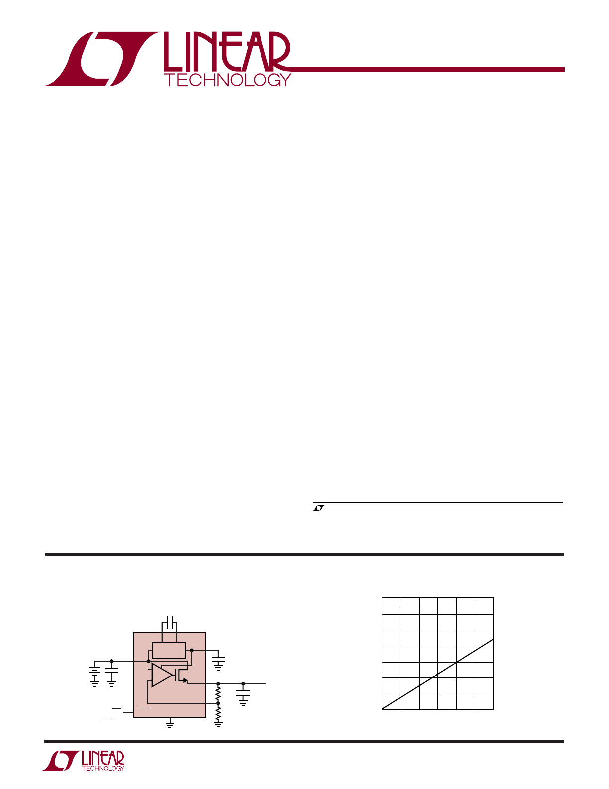
LTC3035
300mA VLDO Linear
Regulator with Charge Pump
Bias Generator
U
DESCRIPTIO
The LTC®3035 is a micropower, VLDO™ (very low dropout) linear regulator which operates from input voltages as
low as 1.7V. The device is capable of supplying 300mA of
output current with a typical dropout voltage of only
45mV. To allow operation at low input voltages the LTC3035
includes a charge pump generator that provides the necessary bias voltage for the internal LDO circuitry. Output
current comes directly from the input supply for high
efficiency regulation. The charge pump bias generator
requires only a 0.1µF flying capacitor and a 1µF bypass
capacitor for operation. The low 0.4V internal reference
voltage allows the LTC3035 to be programmed to much
lower output voltages than commonly available in LDOs.
The output voltage is programmed via two tiny SMD
resistors. The LTC3035’s low quiescent current makes it
an ideal choice for use in battery-powered systems.
Other features include high output voltage accuracy, excellent transient response, stability with ultralow ESR
ceramic capacitors as small as 1µF, short-circuit and
thermal overload protection, output current limiting and
reverse output current protection. The LTC3035 is available in a tiny, low profile (3mm × 2mm × 0.75mm) 8-lead
DFN package.
, LTC and LT are registered trademarks of Linear Technology Corporation.
VLDO is a trademark of Linear Technology Corporation.
All other trademarks are the property of their respective owners.
Protected by U.S. Patents, including 6411531, others pending.
TYPICAL APPLICATIO
3.3V Output Voltage from Li-Ion Battery
0.1µF
CM
CP
BIAS
GENERATOR
Li-Ion
BATTERY
3.4V TO 4.2V
OFF ON
1µF
IN
0.4V
SHDN
+
–
LTC3035
GND
BIAS
OUT
ADJ
U
C
BIAS
1µF
294k
40.2k
3035 TA01a
C
1µF
OUT
V
OUT
3.3V
300mA
Dropout Voltage vs Load Current
70
TA = 25°C
60
50
40
30
20
DROPOUT VOLTAGE (mV)
10
0
0
50 100
200 300
150 250
I
(mA)
OUT
3035 TA01b
3035f
1
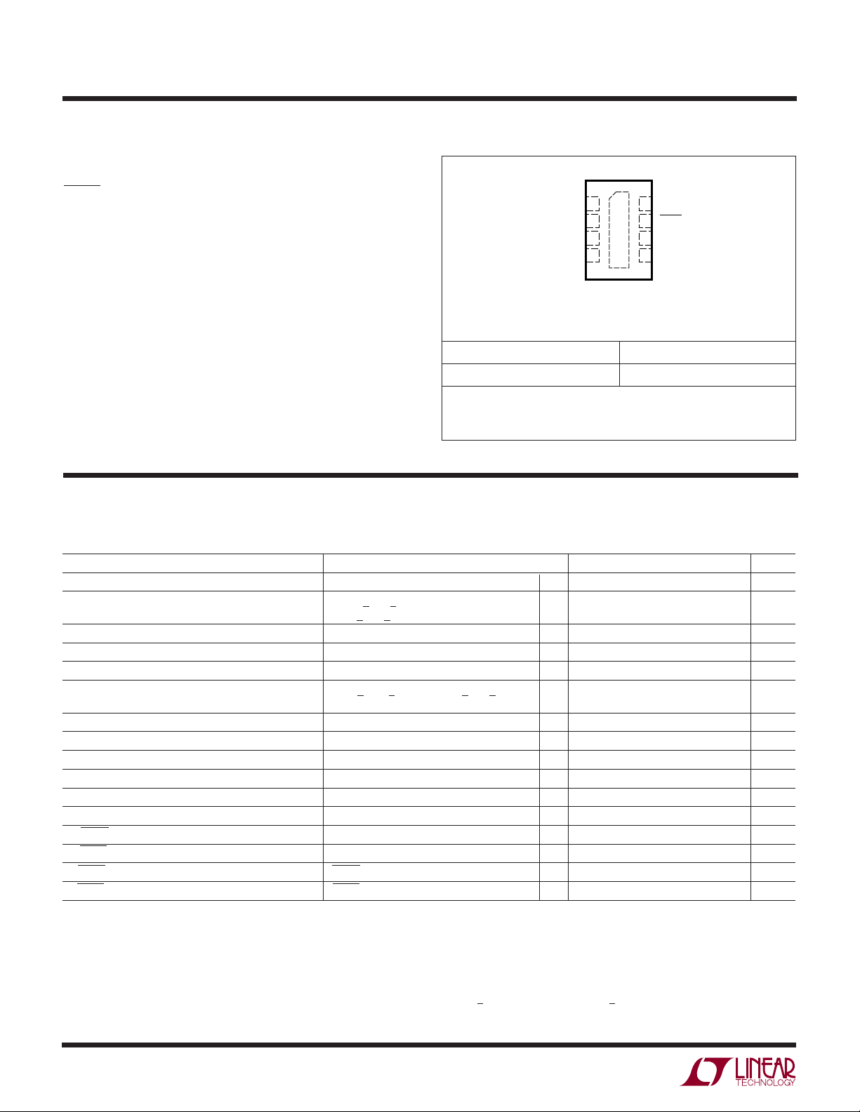
LTC3035
WW
W
ABSOLUTE AXI U RATI GS
U
UUW
PACKAGE/ORDER I FOR ATIO
(Notes 1, 2)
CM
GND
IN
TOP VIEW
1CP
2
3
4
8
BIAS
SHDN
7
9
ADJ
6
OUT
5
VIN to GND.................................................. –0.3V to 6V
SHDN to GND ............................................. –0.3V to 6V
CP, CM, BIAS to GND ................................. –0.3V to 6V
ADJ to GND ................................................ – 0.3V to 6V
to GND ............................................... – 0.3V to 6V
V
OUT
Operating Junction Temperature
(Note 3) ........................................... – 40°C to 125°C
8-LEAD (3mm × 2mm) PLASTIC DFN
Storage Temperature Range ................ –65°C to 125°C
Output Short Circuit Duration .......................... Indefinite
EXPOSED PAD (PIN 9) IS GND,MUST BE SOLDERED TO PCB
ORDER PART NUMBER
LTC3035EDDB
Order Options Tape and Reel: Add #TR
Lead Free: Add #PBF Lead Free Tape and Reel: Add #TRPBF
Lead Free Part Marking: http://www.linear.com/leadfree/
Consult LTC Marketing for parts specified with wider operating temperature ranges.
ELECTRICAL CHARACTERISTICS
range, otherwise specifications are at T
capacitors ceramic) unless otherwise noted.
PARAMETER CONDITIONS MIN TYP MAX UNITS
VIN Operating Voltage (Note 4)
V
Output Voltage Range 2.63V < VIN < 5.5V
BIAS
V
Output Voltage Range
OUT
VIN Operating Current I
VIN Shutdown Current V
V
Regulation Voltage (Note 5) 1mA < I
ADJ
I
ADJ Input Current V
ADJ
OUT Load Regulation (Referred to ADJ Pin) I
Dropout Voltage (Note 6) VIN = 1.7V, V
I
Continuous Output Current
OUT
I
Short Circuit Output Current V
OUT
V
Output Noise Voltage F = 10Hz to 100kHz, I
OUT
VIH SHDN Input High Voltage
VIL SHDN Input Low Voltage
IIH SHDN Input High Current SHDN = V
IIL SHDN Input Low Current SHDN = 0V –1 1 µA
= 25°C. VIN = 3.6V, V
A
1.7V
OUT
SHDN
V
OUT
ADJ
OUT
ADJ
The ● denotes specifications which apply over the full specified temperature
= 3.3V, C
OUT
< VIN < 2.63V
= 10µA
= 0V 1 5 µA
< 300mA, 1.7V < VIN < 5.5V,
OUT
= 1.5V
= 0.4V
= 1mA to 300mA –0.2 mV
= 0.37V, I
ADJ
= V
= 0 760 mA
OUT
OUT
IN
= 0.1µF, C
FLY
= 300mA
OUT
= 150mA 150 µVrms
DDB PACKAGE
T
= 125°C, θJA = 76°C/W
JMAX
DDB PART MARKING
LBRM
= 1µF, CIN = 1µF, C
OUT
●
1.7 5.5 V
●
4.8 5 5.3 V
●
1.85 • VIN 1.90 • VIN 1.95 • V
●
V
ADJ
●
●
0.392 0.4 0.408 V
●
–50 0 50 nA
●
●
300 mA
●
1.1 V
●
–1 1 µA
100 200 µA
= 1µF (all
BIAS
45 100 mV
IN
3.6 V
0.3 V
V
Note 1: Absolute Maximum Ratings are those values beyond which the life
of a device may be impaired.
Note 2: This IC includes overtemperature protection that is intended to
protect the device during momentary overload conditions. Junction
temperature will exceed 125°C when overtemperature protection is active.
Continuous operation above the specified maximum operating junction
temperature may impair device reliability.
2
Note 3: The LTC3035 regulator is tested and specified under pulse load
conditions such that T
25°C. Performance at –40°C and 125°C is assured by design,
characterization and correlation with statistical process control.
Note 4: Min Operating Input Voltage required for regulation is:
> V
V
IN
OUT
≈ TA. The LTC3035 is 100% production tested at
J
+ V
DROPOUT
and VIN > 1.7V
3035f
ELECTRICAL CHARACTERISTICS
LTC3035
Note 5: Operating conditions are limited by maximum junction
temperature. The regulated output voltage specification will not apply for
all possible combinations of input voltage and output current. When
Note 6: Dropout voltage is minimum input to output voltage differential
needed to maintain regulation at a specified output current. In dropout, the
output voltage will be equal to V
operating at maximum input voltage, the output current range must
be limited.
UW
TYPICAL PERFOR A CE CHARACTERISTICS
Dropout Voltage vs Load Current
70
60
50
40
30
20
DROPOUT VOLTAGE (mV)
10
0
0
50 100
TA = 25°C
I
OUT
TA = 125°C
TA = –40°C
200 300
150 250
(mA)
3035 G01
VIN Shutdown Current VIN No Load Operating Current
5.0
4.5
4.0
3.5
3.0
2.5
(µA)
IN
I
2.0
1.5
1.0
0.5
0
0
1
TA = 85°C
TA = –40°C
2
TA = 25°C
34
VIN (V)
5
LT1108 • TPC12
– V
IN
115
V
OUT
110
105
100
(µA)
IN
I
95
90
85
6
80
3
DROPOUT
= 3.3V
3.5 4
.
TA = 125°C
TA = 85°C
TA = 25°C
TA = –40°C
4.5 5.5
VIN (V)
56
3035 G03
VIN No Load Operating Current
120
V
= 1.5V
OUT
110
100
90
(µA)
IN
I
80
70
60
0
TA = 125°C
234
1
VIN (V)
TA = 25°C
TA = –40°C
TA = 85°C
56
3035 G04
404
V
= 3.3V
OUT
403
402
401
400
399
ADJUST VOLTAGE (mV)
398
397
396
–25 15
–45
–5
TEMPERATURE (°C)
ADJ Voltage vs Input VoltageADJ Voltage vs Temperature
404
V
= 1.5V
OUT
403
402
401
400
399
ADJ VOLTAGE (mV)
398
397
95
55
35
115
75
3035 G05
396
0
VIN (V)
5
4
3035 G06
3035f
36
2
1
3
LTC3035
UW
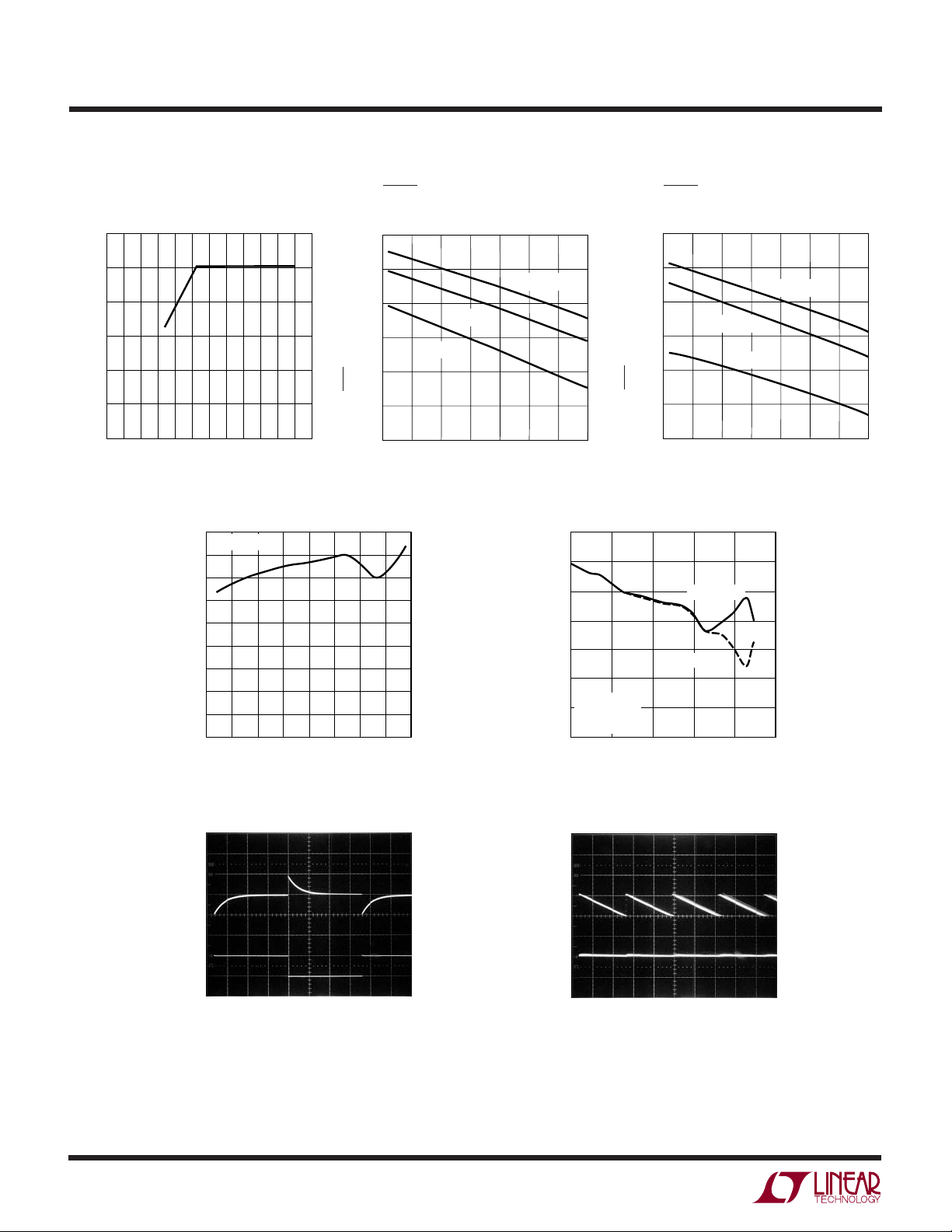
TYPICAL PERFOR A CE CHARACTERISTICS
BIAS Voltage vs Input Voltage
6
5
4
3
2
BIAS VOLTAGE (V)
1
0
0
1
2.5 3.5 4.5 5.5 6
234
1.5
VIN (V)
Current Limit vs Input Voltage
900
V
OUT
800
700
600
500
400
300
CURRENT LIMIT (mA)
200
100
0
1.5
= 0V
2
SHDN Threshold (Rising)
vs Temperature
1000
900
800
700
600
SHDN THRESHOLD (mV)
500
50.5
3035 G07
400
–45
VIN = 1.7V
5
–20
TEMPERATURE (°C)
VIN = 3.6V
VIN = 5.5V
55
30
80
105 130
3035 G08
SHDN Threshold (Falling)
vs Temperature
1000
900
800
700
600
SHDN THRESHOLD (mV)
500
400
–45
VIN = 3.6V
5
–20
TEMPERATURE (°C)
VIN = 1.7V
30
VIN = 5.5V
55
80
105 130
3035 G09
VIN Ripple Rejection vs Frequency
70
60
C
= 10µF
OUT
C
= 1µF
OUT
1M
3035 G13
3
3.5
VIN (V)
50
40
30
REJECTION (dB)
20
VIN = 3.6V
10
= 3.3V
V
OUT
= 100mA
I
OUT
0
42.5
4.5
5.55
3035 G10
1k 10k 100k 10M
100
FREQUENCY (Hz)
4
20mV/DIV
300mA
I
OUT
Transient Response
V
OUT
AC
10mA
= 3.6V
IN
= 3.3V
V
OUT
= 1µF
C
OUT
BIAS Output Ripple
V
BIAS
50mV/DIV
AC
V
OUT
5mV/DIV
AC
200µs/DIVV
3035 G11
V
C
C
C
I
OUT
= 3.6V
IN
OUT
BST
FLY
OUT
= 3.3V
500µs/DIVV
= 1µF
= 0.1µF
= 1µF
= 1mA
3035 G12
3035f

LTC3035
U
UU
PI FU CTIO S
CP (Pin 1): Flying Capacitor Positive Terminal.
CM (Pin 2): Flying Capacitor Negative Terminal.
GND (Pin 3): Ground. Connect to a ground plane.
IN (Pin 4): Input Supply Voltage. The output load current
is supplied directly from IN. The IN pin should be locally
bypassed to ground if the LTC3035 is more than a few
inches away from another source of bulk capacitance. In
general, the output impedance of a battery rises with
frequency, so it is usually adviseable to include an input
bypass capacitor when supplying IN from a battery. A
capacitor of 1µF is usually sufficient.
OUT (Pin 5): Regulated Output Voltage. The OUT pin
supplies power to the load. A minimum ceramic output
capacitor of at least 1µF is required to ensure stability.
Larger output capacitors may be required for applications
with large transient loads to limit peak voltage transients.
See the Applications Information section for more information on output capacitance.
ADJ (Pin 6): Adjust Input Pin. This is the input to the error
amplifier. The ADJ pin reference voltage is 0.4V referenced
to ground. The output voltage range is 0.4V to 3.6V and is
set by connecting ADJ to a resistor divider from OUT to
GND.
SHDN (Pin 7): Shutdown Input, Active Low. This pin is
used to put the LTC3035 into shutdown. The SHDN pin
current is typically less than 10nA. The SHDN pin cannot
be left floating and must be tied to a valid logic level if
not used.
BIAS (Pin 8): BIAS Output Voltage Pin. BIAS is the output
of the charge pump and provides the high side supply for
the LTC3035 LDO circuitry. This pin should be locally
bypassed to ground by a 1µF or greater capacitor as close
as possible to the pin. Nothing else should be connected
to this pin.
Exposed Pad (Pin 9): Ground and Heat Sink. Must be
soldered to PCB ground plane or large pad for optimal
thermal performance.
BLOCK DIAGRA
BIAS
8
1.9 • V
V
IN
4
SHDN
7
BIAS
UVLO
GND
PINS 3, 9
W
5V
SHDN
IN
V
MIN
REFERENCE
0.400V
–
800kHz
EN
+
OSCILLATOR
CHARGE
PUMP
SOFT-START BIAS
+
–
2.5k
CM
OUT
ADJ
CP
1
2
5
6
3035 BD
3035f
5

LTC3035
WUUU
APPLICATIO S I FOR ATIO
(Refer to Block Diagram)
The LTC3035 is a VLDO (very low dropout) linear regulator
which operates from input voltages between 1.7V and
5.5V. The LDO uses an internal NMOS transistor as the
pass device in a source-follower configuration. The internal charge pump generator provides the high supply
necessary for the LDO circuitry while the output current
comes directly from the IN input for high efficiency
regulation.
Charge Pump Operation
The LTC3035 contains a charge pump to produce the
necessary bias voltage supply for the LDO. The charge
pump utilizes Burst Mode operation to achieve high
efficiency for the relatively low current levels needed for
the LDO circuitry. The charge pump requires only a small
0.1µF flying capacitor between the CP and CM pins and a
1µF bypass capacitor at BIAS.
An internal oscillator centered at 800kHz controls the
two-phase switching cycle of the charge pump. During the
first phase a current source charges the flying capacitor
between V
and GND. During the second phase, the
IN
capacitor’s positive terminal connects to BIAS and the
current source drives the capacitor’s minus terminal,
delivering charge to the BIAS bypass capacitor and increasing its voltage.
A burst comparator with hysteresis monitors the voltage
on the BIAS pin. When BIAS is above the upper threshold
of the comparator, the oscillator is disabled and no switching occurs. When BIAS falls below the comparator’s lower
threshold, the oscillator is enabled and the BIAS pin gets
charged. The thresholds of the burst comparator are
dynamically adjusted to maintain a DC level shown by
Figure 1. BIAS regulates to 1.9 • V
or 5V, whichever
IN
voltage is lower. The voltage ripple at BIAS is controlled to
approximately 1% of its DC value.
5
1.9 • V
IN
3.23
BIAS (V)
3035 F01
1.7 2.63
Figure 1. LTC3035 BIAS Voltage vs VIN Voltage
V
(V)
IN
5.5
before the LDO disables. When the LDO is disabled, OUT
is pulled to GND through the external divider and an
internal 2.5k resistor.
The LDO provides a high accuracy output capable of
supplying 300mA of output current with a typical dropout
voltage of only 45mV. A single ceramic capacitor as small
as 1µF is all that is required for output bypassing. The low
reference voltage allows the LTC3035 output to be
programmed from 0.4V to 3.6V.
As shown in the Block Diagram, the charge pump output
at BIAS supplies the LDO circuitry while the output current
comes directly from the IN input for high efficiency
regulation. The low quiescent supply current, IIN = 100µA,
drops to I
= 1µA typical in shutdown making the LTC3035
IN
an ideal choice for use in battery-powered systems.
The device also includes current limit, thermal overload
protection, and reverse output current protection. The fast
transient response of the follower output stage overcomes
the traditional tradeoff between dropout voltage, quiescent current and load transient response inherent in most
LDO regulator architectures. The LTC3035 also includes
overshoot detection circuitry which brings the output back
into regulation when going from heavy to light output
loads (see Figure 2).
LDO Operation
An undervoltage lockout comparator (UVLO) senses the
BIAS voltage to ensure that the BIAS supply for the LDO is
greater than 90% of its regulation value before
enabling the LDO. Once the LDO gets enabled, the UVLO
threshold switches to 50% of its regulation value. Thus the
BIAS voltage must fall below 50% of its regulation voltage
6
The LTC3035 also includes a soft-start feature to prevent
excessive current flow during start-up. After the BIAS
voltage reaches regulation, the soft-start circuitry gradually increases the LDO reference voltage from 0V to 0.4V
over a period of about 600µs. There is a short 700µs delay
from the time BIAS reaches regulation until the LDO
output starts to rise (see Figure 3).
3035f

WUUU
APPLICATIO S I FOR ATIO
LTC3035
V
OUT
20mV/DIV
AC
300mA
I
OUT
0mA
3035 F02
V
C
= 3.6V
IN
OUT
OUT
= 3.3V
200µs/DIVV
= 1µF
Figure 2. Output Step Response
ON
SHDN
OFF
V
BIAS
2V/DIV
0V
V
OUT
2V/DIV
0V
3035 F03
V
C
C
= 3.6V
IN
OUT
OUT
BIAS
= 3.3V
= 1µF
= 1µF
500µs/DIVV
Figure 3. Bias and Output Start-Up Waveforms
Adjustable Output Voltage
The output voltage is set by the ratio of two external
resistors as shown in Figure 4. The device servos the
output to maintain the ADJ pin voltage at 0.4V (referenced
to ground). Thus the current in R1 is equal to 0.4V/R1. For
good transient response, stability and accuracy the
current in R1 should be at least 8µA, thus the value of R1
should be no greater than 50k. The current in R2 is the
current in R1 plus the ADJ pin bias current. Since the ADJ
pin bias current is typically <10nA it can be ignored in the
output voltage calculation. The output voltage can be
calculated using the formula in Figure 4. Note that in
shutdown the output is turned off and the divider current
will be zero once C
is discharged.
OUT
The LTC3035 operates at a relatively high gain of
–0.7µV/mA referred to the ADJ input. Thus a load
V
ADJ
GND
OUT
V
OUT
R2
C
OUT
R1
3035 F04
R2
1 +
= 0.4V
()
R1
Figure 4. Programming the LTC3035
current change of 1mA to 300mA produces a –0.2mV
drop at the ADJ input. To calculate the change refered to
the output simply multiply by the gain of the feedback
network (i.e., 1 + R2/R1). For example, to program the
output for 3.3V choose R2/R1 = 7.25. In this example an
output current change of 1mA to 300mA produces
–0.2mV • (1 + 7.25) = 1.65mV drop at the output.
Output Capacitance and Transient Response
The LTC3035 is designed to be stable with a wide range of
ceramic output capacitors. The ESR of the output capacitor affects stability, most notably with small capacitors. An
output capacitor of 1µF or greater with an ESR of 0.05Ω or
less is recommended to ensure stability. The LTC3035 is
a micropower device and output transient response will be
a function of output capacitance. Larger values of output
capacitance decrease the peak deviations and provide
improved transient response for larger load current
changes. Note that bypass capacitors used to decouple
individual components powered by the LTC3035 will
increase the effective output capacitor value. High ESR
tantalum and electrolytic capacitors may be used, but a
low ESR ceramic capacitor must be in parallel at the
output. There is no minimum ESR or maximum capacitor
size requirements.
Extra consideration must be given to the use of ceramic
capacitors. Ceramic capacitors are manufactured with a
variety of dielectrics, each with different behavior across
temperature and applied voltage. The most common dielectrics used are Z5U, Y5V, X5R and X7R. The Z5U and
Y5V dielectrics are good for providing high capacitances
in a small package, but exhibit strong voltage and temperature coefficients as shown in Figures 5 and 6. When
used with a 3.3V regulator, a 1µF Y5V capacitor can lose
as much as 80% of its rated capacitance over the operating
3035f
7

LTC3035
WUUU
APPLICATIO S I FOR ATIO
20
0
–20
–40
–60
CHANGE IN VALUE (%)
–80
–100
0
Figure 5. Ceramic Capacitor DC Bias Characteristics
20
0
–20
–40
–60
CHANGE IN VALUE (%)
–80
BOTH CAPACITORS ARE 1µF,
6.3V, 0402 CASE SIZE
–100
–50
Figure 6. Ceramic Capacitor Temperature Characteristics
BOTH CAPACITORS ARE 1µF,
6.3V, 0402 CASE SIZE
X5RY5V
13
2
DC BIAS VOLTAGE (V)
02550
–25
TEMPERATURE (°C)
45
Y5V
6
3035 F05
X5R
75
3035 F06
temperature range. The X5R only loses about 40% of its
rated capacitance over the operating temperature range.
The X5R and X7R dielectrics result in more stable characteristics and are more suitable for use as the output
capacitor. The X7R type has better stability across temperature and bias voltage, while the X5R is less expensive
and is available in higher values. In all cases, the output
capacitance should never drop below 0.4µF, or instability
or degraded performance may occur.
available current, a 0.1µF or greater ceramic capacitor
should be used.
Warning: A polarized capacitor such as
tantalum or aluminum should never be used for the flying
capacitor since its voltage can reverse upon start-up of the
LTC3035. Low ESR ceramic capacitors should always be
used for the flying capacitor.
A 1µF or greater low ESR (<0.1Ω) ceramic capacitor is
recommended to bypass the BIAS pin. Larger values of
capacitance will not reduce the size of the BIAS ripple
much, but will decrease the ripple frequency proportionally. The BIAS pin should maintain 0.4µF of capacitance at
all times to ensure correct operation. High ESR tantalum
and electrolytic capacitors may be used, but a low ESR
ceramic must be used in parallel for correct operation. It
is also recommended that IN be bypassed to ground with
a 1µF or greater ceramic capacitor.
Thermal Considerations
The power handling capability of the device will be limited
by the maximum rated junction temperature (125°C). The
power dissipated by the device will be the output current
multiplied by the input/output voltage differential:
(I
)(VIN – V
OUT
OUT
)
The LTC3035 has internal thermal limiting designed to
protect the device during momentary overload conditions.
For continuous normal conditions, the maximum junction
temperature rating of 125°C must not be exceeded. It is
important to give careful consideration to all sources of
thermal resistance from junction to ambient. Additional
heat sources mounted nearby must also be considered.
For surface mount devices, heat sinking is accomplished
by using the heat-spreading capabilities of the PC board
and its copper traces. Copper board stiffeners and plated
through holes can also be used to spread the heat
generated by power devices.
Charge Pump Component Selection
The flying capacitor controls the strength of the charge
pump. In order for the charge pump to deliver its maximum
8
A junction to ambient thermal coefficient of 76°C/W is
achieved by connecting the Exposed Pad of the DFN
package directly to a ground plane of about 2500mm2.
3035f

OPERATIO
C
BIAS
BIAS
3035 F07
SHDN
OUT
ADJ
IN
GND
CM
CP
CF
R2
VIA CONNECTION
TO GND PLANE
R1
C
OUT
C
IN
4
3
2
1
5
6
7
8
LTC3035
U
Calculating Junction Temperature
Example: Given an output voltage of 1.5V, an input voltage
of 1.8V to 3V, an output current range of 0mA to 100mA
and a maximum ambient temperature of 50°C, what will
the maximum junction temperature be?
The power dissipated by the device will be approximately:
I
OUT(MAX)(VIN(MAX)
– V
OUT
)
overstress condition is removed. Long term overstress
(T
>125°C) should be avoided as it can degrade the
J
performance or shorten the life of the part.
Layout Considerations
Connection from the BIAS and OUT pins to their respective
ceramic bypass capacitor should be kept as short as
possible. The ground side of the bypass capacitors should
be connected directly to the ground plane for best results
where:
I
OUT(MAX)
= 100mA
or through short traces back to the GND pin of the part.
Long traces will increase the effective series ESR and
inductance of the capacitor which can degrade
V
IN(MAX)
so:
P = 100mA(3V – 1.5V) = 0.15W
Even under worst-case conditions LTC3035’s BIAS pin
power dissipation is only about 1mW, thus can be
ignored. The junction to ambient thermal resistance will be
on the order of 76°C/W. The junction temperature rise
above ambient will be approximately equal to:
0.15W(76°C/W) = 11.4°C
The maximum junction temperature will then be equal to
the maximum junction temperature rise above ambient
plus the maximum ambient temperature or:
= 3V
performance.
The CP and CM pins of the charge pump are switching
nodes. The transition edge rates of these pins can be quite
fast (~10ns). Thus care must be taken to make sure these
nodes do not couple capacitively to other nodes (especially the ADJ pin). Place the flying capacitor as close as
possible to the CP and CM pins for optimum charge pump
performance.
Because the ADJ pin is relatively high impedance
(depending on the resistor divider used), stray capacitance at this pin should be minimized (<10pF) to prevent
phase shift in the error amplifier loop. Additional special
attention should be given to any stray capacitances that
can couple external signals onto the ADJ pin producing
T = 50°C + 11.4°C = 61.4°C
undesirable output ripple. For optimum performance
connect the ADJ pin to R1 and R2 with a short PCB trace
Short-Circuit/Thermal Protection
The LTC3035 has built-in output short-circuit current
and minimize all other stray capacitance to the ADJ pin.
Figure 7 shows an example layout for the LTC3035.
limiting as well as over temperature protection. During
short-circuit conditions, internal circuitry automatically
limits the output current to approximately 760mA. At
higher temperatures, or in cases where internal power
dissipation causes excessive self heating on chip, the
thermal shutdown circuitry will shut down the charge
pump and LDO when the junction temperature exceeds
approximately 155°C. It will reenable the converter and
LDO once the junction temperature drops back to approximately 140°C. The LTC3035 will cycle in and out of
thermal shutdown without latch-up or damage until the
Figure 7. Suggested Layout
3035f
9

LTC3035
TYPICAL APPLICATIO
3
SW1
= 2.7V TO 4.2V
V
Li-Ion
OFF ON
IN
S
+
C1
10µF
7
V
IN
8
SHDN/SS
2
MODE/SYNC
*
1
R
T
R
T
60.4k
SS
S
U
L1
10µH
LTC3440
Low Noise Li-Ion to 3.3V Supply
S S
4
SW2
V
GND
OUT
FB
V
C
6
9
C5 1.5nF
10
5
S S
R1
357k
S
S
R3
15k
R2
200k
S
S
C2
22µF
3035 TA02
600mA
C
IN
1µF
3.4V
CP
IN
LTC3035
SHDN
GND
*1 = Burst Mode OPERATION
0 = FIXED FREQUENCY
C1: TAIYO YUDEN JMK212BJ106MG
C2: TAIYO YUDEN JMK325BJ226MM
, C
C
L1: SUMIDA CDRH6D38-100
, C
IN
BIAS
0.1µF
CM
BIAS
OUT
ADJ
: TDK C1005X5R0J105K
OUT
C
BIAS
1µF
V
= 3.3V
S
S
S
294k
40.2k
C
1µF
OUT
I
OUT
OUT
≤ 300mA
Efficiency vs Output Current Ripple Rejection
100
90
80
Burst Mode
70
OPERATION
60
50
40
EFFICIENCY (%)
30
20
10
0
0.1
Burst Mode IS A REGISTERED TRADEMARK OF
LINEAR TECHNOLOGY CORPORATION
VIN = 2.7V
®
VIN = 4.2V
VIN = 3.6V
1
OUTPUT CURRENT (mA)
10
100
3035 TA02b
1000
LTC3440
OUTPUT
20mV/DIV
LTC3035
OUTPUT
20mV/DIV
AC
AC
OUT
= 25mA
20µs/DIVI
3035 TA02c
10
3035f

PACKAGE DESCRIPTIO
0.61 ±0.05
(2 SIDES)
2.55 ±0.05
1.15 ±0.05
0.25 ± 0.05
RECOMMENDED SOLDER PAD PITCH AND DIMENSIONS
U
DDB Package
8-Lead Plastic DFN (3mm × 2mm)
(Reference LTC DWG # 05-08-1702 Rev B)
0.70 ±0.05
PACKAGE
OUTLINE
0.50 BSC
2.20 ±0.05
(2 SIDES)
LTC3035
PIN 1 BAR
TOP MARK
(SEE NOTE 6)
0.200 REF
3.00 ±0.10
(2 SIDES)
2.00 ±0.10
(2 SIDES)
0.75 ±0.05
NOTE:
1. DRAWING CONFORMS TO VERSION (WECD-1) IN JEDEC PACKAGE OUTLINE M0-229
2. DRAWING NOT TO SCALE
3. ALL DIMENSIONS ARE IN MILLIMETERS
4. DIMENSIONS OF EXPOSED PAD ON BOTTOM OF PACKAGE DO NOT INCLUDE
MOLD FLASH. MOLD FLASH, IF PRESENT, SHALL NOT EXCEED 0.15mm ON ANY SIDE
5. EXPOSED PAD SHALL BE SOLDER PLATED
6. SHADED AREA IS ONLY A REFERENCE FOR PIN 1 LOCATION ON THE TOP AND BOTTOM OF PACKAGE
R = 0.05
0 – 0.05
0.56 ± 0.05
(2 SIDES)
R = 0.115
TYP
TYP
0.25 ± 0.05
2.15 ±0.05
(2 SIDES)
BOTTOM VIEW—EXPOSED PAD
0.40 ± 0.10
85
14
0.50 BSC
PIN 1
R = 0.20 OR
0.25 × 45°
CHAMFER
(DDB8) DFN 0905 REV B
Information furnished by Linear Technology Corporation is believed to be accurate and reliable.
However, no responsibility is assumed for its use. Linear Technology Corporation makes no representation that the interconnection of its circuits as described herein will not infringe on existing patent rights.
3035f
11

LTC3035
TYPICAL APPLICATIO S
V
IN
2.5V
0.1µF
U
Dual LDO Output (1.8V, 1.5V) from 2.5V Supply Rail
OFF ON
OFF ON
V
1.8V
CP CM
IN
LTC3035
SHDN
GND
BIAS
OUT
ADJ
1µF1µF
140k
40.2k
1µF
V
I
OUT
OUT
= 1.8V
< 300mA
IN
LTC3025
SHDN
GND
BIAS
OUT
ADJ
0.1µF0.1µF
110k
40.2k
1µF
3035 TA03
V
OUT
I
OUT
= 1.5V
< 300mA
Dual LDO Output (1.5V, 1.2V) from 1.8V Supply Rail
IN
0.1µF
CP CM
IN
LTC3035
SHDN
GND
BIAS
OUT
ADJ
1µF1µF
110k
40.2k
1µF
V
I
OUT
OUT
= 1.5V
< 300mA
IN
LTC3025
SHDN
GND
BIAS
OUT
ADJ
0.1µF0.1µF
80k
40.2k
1µF
3035 TA04
V
OUT
I
OUT
= 1.2V
< 300mA
RELATED PARTS
PART NUMBER DESCRIPTION COMMENTS
LT®1761 100mA, Low Noise Micropower, LDO VIN: 1.8V to 20V, V
1.5V, 1.8V, 2V, 2.5V, 2.8V, 3V, 3.3V, 5V, ThinSOT
Low Noise < 20µV
LT1762 150mA, Low Noise Micropower LDO VIN: 1.8V to 20V, V
2.5V, 3V, 3.3V, 5V, MS8 Package. Low Noise < 20µV
LT1763 500mA, Low Noise Micropower LDO VIN: 1.8V to 20V, V
1.8V, 2.5V, 3V, 3.3V, 5V, S8 Package. Low Noise < 20µV
LTC1844 150mA, Very Low Dropout LDO VIN: 1.6V to 6.5V, V
1.5V, 1.8V, 2.5V, 2.8V, 3.3V, ThinSOT Package. Low Noise < 30µV
1µF Ceramic Capacitors
LT1962 300mA, Low Noise Micropower LDO VIN: 1.8V to 20V, V
1.8V, 2.5V, 3V, 3.3V, 5V, MS8 Package. Low Noise < 20µV
LT3020 100mA, Low Voltage, VLDO VIN: 0.9V to 10V, V
DFN, MS8 Package
LTC3025 300mA, Micropower VLDO Linear Regulator VIN: 0.9V to 5.5V, V
I
< 1µA, V
SD
= Adj, DFN Package. Stable with 1µF Ceramic Capacitors
OUT
LTC3026 1.5A, Low Input Voltage VLDO Linear Regulator VIN: 1.14V to 3.5V (Boost Enabled), 1.14V to 5.5V (External 5V Boost),
V
= 0.4V, VDO = 0.15V, IQ = 400µA, ISD < 1µA, V
OUT(MIN)
DFN, MSOP Packages. Stable with 10µF Ceramic Capacitors
ThinSOT is a trademark of Linear Technology Corporation.
Linear Technology Corporation
12
1630 McCarthy Blvd., Milpitas, CA 95035-7417
(408) 432-1900 ● FAX: (408) 434-0507
●
www.linear.com
= 1.22V, VDO = 0.30V, IQ = 20µA, ISD < 1µA, V
OUT(MIN)
, Stable with 1µF Ceramic Capacitors
RMSP-P
= 1.22V, VDO = 0.30V, IQ = 25µA, ISD < 1µA, V
OUT(MIN)
= 1.22V, VDO = 0.30V, IQ = 30µA, ISD < 1µA, V
OUT(MIN)
= 1.25V, VDO = 0.08V, IQ = 40µA, ISD < 1µA, V
OUT(MIN)
= 1.22V, VDO = 0.27V, IQ = 30µA, ISD < 1µA, V
OUT(MIN)
= 0.20V, VDO = 0.15V, IQ = 120µA, ISD < 3µA, V
OUT(MIN)
: 2.5V to 5.5V, V
BIAS
OUT(MIN)
TM
Package.
RMSP-P
= 0.4V, VDO = 0.05V, IQ = 54µA,
© LINEAR TECHNOLOGY CORPORATION 2005
RMSP-P
RMSP-P
RMSP-P
= Adj,
OUT
LT 1105 • PRINTED IN USA
= Adj,
OUT
= Adj,
OUT
= 1.5,
OUT
= Adj,
OUT
, Stable with
= 1.5,
OUT
= Adj,
OUT
3035f
 Loading...