


L DESIGN FEATURES
R1
1%
R2
1%
VREF
VPG
GND
LTC2931
+
–
0.5V
V3, V4,
V5 OR V6
V
TRIP
R3
1%
R4
1%
LTC2931
V4
VREF
V
TRIP
R4
1%
R3
1%
LTC2931
6-Input Supervisors Offer Accurate
Monitoring and 125°C Operation
by Shuley Nakamura and Al Hinckley
Introduction
The latest trio of power supply supervisors from Linear Technology is ideal
for today’s multi-voltage systems that
require accurate supply monitoring.
The LTC2930, LTC2931, and LTC2932
are 6-input voltage monitors capable of
maintaining 1.5% threshold accuracy
from –40°C to 125°C. The combination of monitored supply voltages is
set by a single pin. Each part offers
16 threshold voltage combinations,
thus meeting the needs of almost
any multi-voltage system. This programmability eliminates the need to
qualify, source and stock unique part
numbers for different threshold voltage
combinations.
The overall architecture and operating specifications of these three
devices are similar, but each has
unique features (see Table 1). The
LTC2930 generates a reset after
any undervoltage event or when the
manual reset input (MR) pulls low. It
is ideal for space-constrained applications as it comes in a compact 3mm
× 3mm 12-lead DFN package. The
LTC2931 includes a watchdog input
(WDI), a watchdog output (WDO) and
user-adjustable watchdog periods to
enable microprocessor monitoring
and control. The LTC2932 can vary
its monitor thresholds from 5% to
12.5%, and a reset disable pin provides margining capability. Both the
LTC2931 and LTC2932 are packaged
in 20-pin TSSOP packages and have
separate comparator outputs, enabling individual supply monitoring
and/or sequencing.
Feature LTC2930 LTC2931 LTC2932
Configurable Input
Threshold Combinations
Threshold Accuracy 1.5% 1.5% 1.5%
Adjustable Reset Time
Buffered Reference
Individual Comparator
Outputs
Manual Reset
Independent Watchdog
Circuitry
Reset Disable
Supply Tolerance Fixed, 5% Fixed, 5%
Package
Single Pin Configuration
Makes Life Easy
These supervisors offer an elegant
method of configuring the input voltage thresholds. Figure 1 shows how a
single resistive divider at the VPG pin
sets the supervisor into one of the 16
threshold options shown in Table 2.
See the data sheet for suggested modesetting resistor values.
The actual thresholds are set by
integrated precision dividers for 5V,
Table 1. LTC2930, LTC2931, LTC2932 feature summary
16 16 16
L L L
L L L
L L
L
L
User Selectable
5%, 7.5%, 10%, 12.5%
12-lead
3mm × 3mm DFN
20-lead
F Package
3.3V, 3V, 2.5V, 1.8V, and 1.5V supply
monitoring. For other supply values,
uncommitted comparators with 0.5V
thresholds allow virtually any positive
supply to be monitored using a resistive divider, as shown in Figure 2a.
The V4 input also monitors negative
voltages—with the same 1.5% accuracy—using the integrated buffered
reference for offset (see Figure 2b).
20-lead
F Package
L
10
Figure 1. Mode selection
2a. 2b.
Figure 2. Using a resistive divider to set the voltage trip point
Linear Technology Magazine • March 2008
DESIGN FEATURES L
5V
4.75V
4.675V
±1.5%
THRESHOLD
BAND
4.6V
NOMINAL
SUPPLY
VOLTAGE
SUPPLY TOLERANCE
MINIMUM
RELIABLE
SYSTEM
VOLTAGE
IDEAL
SUPERVISOR
THRESHOLD
REGION OF POTENTIAL MALFUNCTION
–5%
–6.5%
–8%
What Does Threshold
Accuracy Mean?
Consider a 5V system with ±5% supply tolerance. The 5V supply may vary
between 4.75V to 5.25V. System ICs
powered by this supply must operate
reliably within this band (and a little
more, as explained below). A perfectly
accurate supervisor for this supply
generates a reset at exactly 4.75V.
However, no supervisor is this perfect.
The actual reset threshold of a supervisor fluctuates over a specified band;
the LTC2930, LTC2931 and LTC2932
vary ±1.5% around their nominal
threshold voltage over temperature
(Figure 3). The reset threshold band
and the power supply tolerance bands
should not overlap. This prevents false
or nuisance resets when the power
supply is actually within its specified
tolerance band.
The L TC 2930, LT C293 1 and
LTC2932 boast a ±1.5% reset thresh-
old accuracy, so a “5%” threshold is
usually set to 6.5% below the nominal
input voltage. Therefore, a typical
5V, “5%” threshold is 4.675V. The
threshold is guaranteed to lie in the
band between 4.750V and 4.600V
over temperature. The powered system must work reliably down to the
low end of the threshold band, or risk
malfunction before a reset signal is
properly issued.
A less accurate supervisor increases
the required system voltage margin
and increases the probability of system
malfunction. The tight ±1.5% accuracy
specification of the LTC2930, LTC2931
Linear Technology Magazine • March 2008
Figure 3. Tight 1.5% threshold accuracy yields high system reliability
Table 2. Voltage threshold modes
V1 (V) V2 (V) V3 (V) V4 (V) V5 (V) V6 (V)
5.0 3.3 2.5 1.8 ADJ ADJ
5.0 3.3 2.5 1.5 ADJ ADJ
5.0 3.3 2.5 ADJ ADJ ADJ
5.0 3.3 1.8 ADJ ADJ ADJ
5.0 3.3 1.8 –ADJ ADJ ADJ
5.0 3.3 ADJ ADJ ADJ ADJ
5.0 3.3 ADJ –ADJ ADJ ADJ
5.0 3.0 2.5 ADJ ADJ ADJ
5.0 3.0 1.8 ADJ ADJ ADJ
5.0 3.0 ADJ ADJ ADJ ADJ
3.3 2.5 1.8 1.5 ADJ ADJ
3.3 2.5 1.8 ADJ ADJ ADJ
3.3 2.5 1.8 –ADJ ADJ ADJ
3.3 2.5 1.5 ADJ ADJ ADJ
3.3 2.5 ADJ ADJ ADJ ADJ
3.3 2.5 ADJ –ADJ ADJ ADJ
and LTC2932 improves the reliability
of the system over supervisors with
wider threshold specifications.
coupling from other signals. If the
monitored voltage is near or at the reset threshold voltage, this noise could
cause spurious resets. Fortunately,
Glitch Immunity =
No Spurious Resets!
Monitored supply voltages are far from
being ideal, perfectly flat DC signals.
Riding on top of these supplies are
high frequency components caused
by a number of sources such as the
output ripple of the power supply or
the LTC2930, LTC2931 and LTC2932
have been designed with this potential
issue in mind, so spurious resets are
of little to no concern.
Some supply monitors overcome
spurious resets by adding hysteresis
to the input comparator. The amount
of applied hysteresis is stated as
a percentage of the trip threshold.
Unfortunately, this degrades monitor
accuracy because the true accuracy
of the trip threshold is now the percentage of added hysteresis plus the
advertised accuracy of the part. The
LTC2930, LTC2931 and LTC2932 do
not use hysteresis, but instead use
an integration scheme that requires
transients to possess enough magnitude and duration to switch the
comparators. This suppresses spurious resets without degrading the
monitor accuracy.
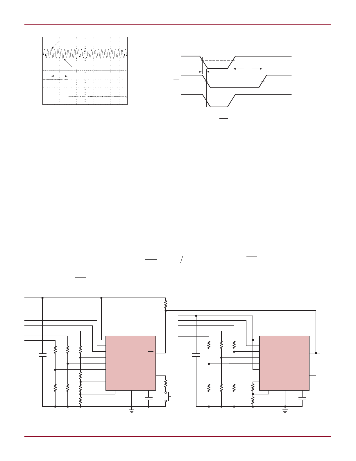
The COMP5 comparator output
response to a “noisy” input on the
LTC2931 is demonstrated in Figure 4.
11
L DESIGN FEATURES
C
t
M
pF ms t
RT
RST
RST
= =
( )
2
500
Ω
•
t
RST
V
RT
V
n
RST
COMP
n
t
UV
300µs PROPAGATION DELAY
–2mV DC STEP APPLIED HERE
500mV
100mV
P–P
V5
100mV/DIV
COMP5
LTC2930
1V
0.9V
–5.2V
1.8V
3.3V
5V
C
RT
47nF
MR
RST
VREF
VPG
GND CRT
V1
V2
V3
V4
V5
V6
121k
1%
R1A
16.2k
1%
R2A
86.6k
1%
100k
1%
10k**
10k
100k
1%
487k
1%
86.6k
1%
68.1k
1%
0.1MF
LTC2930
6V
8V
12V
3V
5V
C
RT
47nF
MANUAL RESET
PUSHBUTTON
t
RST
= 94ms
**OPTIONAL FOR EXTENDED ESD TOLERANCE
MR
RST RESET
VREF
VPG
GND CRT
V1
V2
V3
V4
V5
V6
100k
1%
R1B
40.2k
1%
R2B
59k
1%
100k
1%
100k
1%
2150k
1%
1400k
1%
1020k
1%
0.1MF
Figure 4. Comparator output is
resistant to noisy input voltage
In the example shown, a 500kHz,
100mV
sine wave centered at
P–P
500mV is applied to the V5 input. The
threshold voltage of the adjustable
input, V5, is 500mV. Even though
the signal amplitude goes as low as
450mV, COMP5 remains high. Next,
the DC level of the input is dropped
2mV. In response, COMP5 pulls low
and remains low. As mentioned earlier,
only transients of long enough duration
and magnitude trigger the comparator
output to pull high or low.
Adjustable Reset Timeout Period
for Varied Application Needs
Each of the supervisors includes an
adjustable reset timeout period, t
RST
.
Once all the inputs are above their
threshold values, the reset timer is
started (Figure 5). RST stays low for
Figure 5. RST timing diagram
the duration of t
and remains low
RST
as long as the time between transients
is less than the reset timeout. In other
words, the reset timeout prevents supply transients with frequencies greater
than 1/t
from causing undesired
RST
toggling at the RST output. Keeping
RST low during these supply transients
suppresses spurious resets.
The reset timeout period is adjustable to accommodate a variety of
microprocessor applications. Configure the reset timeout period, t
RST
, by
connecting a capacitor, CRT, between
the CRT pin and GND. The value of
this capacitor is determined by
Leaving the CRT pin unconnected
generates a minimum reset timeout of
approximately 25µs. Maximum reset
timeout is limited by the largest available low leakage capacitor.
Additional Glitch Filtering
Even though all six comparators
have built-in glitch filtering, adding
bypass capacitors on the V1 and V2
inputs is recommended, because of
these two, the input with the higher
voltage functions as VCC for the entire
chip. Additional filter capacitors may
be added to the V3, V4, V5 and V6
inputs if needed to suppress troublesome noise.
Open-Drain Reset
The RST outputs on the LTC2930,
LTC2931 and LTC2932 are opendrain and contain weak pull-up
current sources to the V2 voltage.
Figure 6. Wired-OR system reset
12
Linear Technology Magazine • March 2008

DESIGN FEATURES L
COMP1 COMP2 COMP3 COMP4 COMP5 COMP6
LTC2932
12V (9.6V THRESHOLD)
12V
SUPPLY
STATUS
DONE
2.5V
–5.2V
1.8V
3.3V
5V
365k1%487k
1%
5V
10k 10k
10k
0.1MF
t
RST
= 9.4ms
4.7nF
RDIS
T0
T1
VPG
GND
CRT
V1
V2
V3
V4
V5
RST
V6
VREF
SYSTEM
LOGIC
10k
LT3028
V
IN
3.3V
V
OUT
SHDN
LTM4600
V
IN
V
OUT
RUN
10k
LT3028
V
IN
1.8V
V
OUT
SHDN
10k
LTC3704
V
IN
–5.2V
V
OUT
RUN/UVLO
10k
LT3028
V
IN
2.5V
V
OUT
SHDN
100k1%121k
1%
1820k
1%
100k
1%
R1
16.2k
1%
R2
86.6k
1%
LTC2950-1
V
IN
INT
PB
KILL
EN
The open-drain structure provides
many advantages. For instance, each
of these outputs can be externally
pulled-up to voltages higher than V2
using a pull-up resistor. This facilitates
the use of multiple devices operating
under different I/O voltages. In addition, multiple open-drain outputs can
be configured in a “wired-OR” format
where the outputs are tied together.
Figure 6 showcases two LTC2930
supervisors, whose open-drain RST
outputs are tied together and pulledup to 5V via a 10k pull-up resistor.
If one RST output pulls low due to a
reset event, it sinks current and pulls
the other output low.
Linear Technology Magazine • March 2008
13
multi-voltage systems where it is
important to know which particular
supply has failed.
The individual comparator outputs
also allow power supply sequencing.
Figure 7 shows the LTC2932 in a
5-supply power-up sequencer. As
an input reaches its threshold, the
respective comparator output pulls
high and enables the next DC/DC
converter.
The LTC2950-1 is used to provide
pushbutton control for the sequencer.
After the pushbutton is pressed, the
LTC2950-1 pulls the RUN pin of the
LTM4600 high. Subsequently, the
LTM4600 generates a 5V output which
Figure 7. Five supply 12.5% tolerance power-up sequencer with pushbutton
Comparator Outputs Enable
Individual Supply Monitoring
and Sequencing Support
Real-time comparator outputs on both
the LTC2931 and LTC2932 indicate
the status of the individual inputs.
Similar to the RST output, the comparator outputs are also open-drain
and have weak pull-up current sources
to the V2 voltage.
While RST pulls low when an
undervoltage event occurs on any of
the monitored supplies, a comparator
output pulls low only when its counterpart input is below its threshold
voltage. The ability to monitor the
status of each supply is useful in

L DESIGN FEATURES
t
RST
t
WP
t < t
RST
t
WD
t
WD
RST
WDI
WDO
t
RST
t
RST
t
WD
A. UNDERVOLTAGE EVENT OCCURS, RST PULLS LOW, WDO PULLS HIGH, AND RST TIMER STARTS.
B. RST TIMES OUT (ALL INPUT VOLTAGES BECOME GOOD BEFORE RST TIMEOUT), t
RST
, THEN WATCHDOG TIMER STARTS.
C. WATCHDOG TIMES OUT, tWD, AND WDO PULLS LOW. RST TIMER STARTS.
D. WDI TRANSITION OCCURS BEFORE RST TIMEOUT. WDO PULLS HIGH AND WDO TIMER STARTS.
E. WDI TRANSITION OCCURS WHILE WDO IS HIGH. WATCHDOG TIMER CLEARS AND RESTARTS.
F. WATCHDOG TIMES OUT. WDO PULLS LOW AND RST TIMER STARTS.
G. RST TIMES OUT. WDO PULLS HIGH AND WATCHDOG TIMER STARTS.
A B C D E F G
t
RST
t
RST
t
MRW
V
RT
V
n
RST
MR
t
UV
t
MRD
C
t
M
pF ms t
WT
WD
WD
= =
( )
2050Ω
•
supplies power to each of the four
DC/DC converters.
Three Supervisor Flavors
LTC2930: Manual Reset (MR)
Forces RST Low
Use the manual reset input (MR) on
the LTC2930 to issue a forced reset,
independent of input voltage levels. A
10µA (typical) internal current source
pulls the MR pin to VCC. A logic low on
this pin pulls RST low. When the MR
pin returns high, RST returns high
after the selected reset timeout period
has elapsed, assuming all six voltage
inputs are above their thresholds
(Figure 8). The input-high threshold
on the MR pin is 1.6V (max), allowing
the pin to be driven by low voltage
logic as well.
LTC2931: Monitor a Microprocessor
with the Watchdog Function
The LTC2931’s independent watchdog
circuitry monitors a microprocessor’s
activity. The microprocessor is required to change the logic state of the
WDI pin on a periodic basis in order to
clear the watchdog timer. The LTC2931
consists of a watchdog input (WDI), a
watchdog output (WDO) and a timing
pin (CWT), which allows for a user
adjustable watchdog timeout period.
Figure 9 illustrates the watchdog timer
and its relationship to the reset timer
and WDI.
The watchdog timeout period is
adjustable and can be optimized for
software execution. The watchdog
Figure 8. MR timing diagram
timeout period, tWD, is adjusted by
connecting a capacitor, CWT, between
the CWT pin and ground. The value of
this capacitor is determined by
Leaving the CWT pin unconnected
generates a minimum watchdog timeout of approximately 200µs. Maximum
watchdog timeout is limited by the largest available low leakage capacitor.
LTC2932: Margining Capabilities
and Wider Threshold Tolerances
In high reliability system manufacturing and testing, it is important to
verify that the components will con-
Table 3. LTC2932 Tolerance Selection
T0 T1
TOLERANCE
(%)
Low Low 5 1.210
Low High 7.5 1.175
High Low 10 1.146
High High 12.5 1.113
V
REF
(V)
tinue to operate at or below the rated
power supply tolerance. Verification
usually involves margining the power
supplies, running their outputs at or
beyond rated tolerances. The LTC2932
is designed to complement such testing
in two ways. First, the RST output can
be disabled by pulling RDIS low. In this
state, the RST output remains high
despite any undervoltage events which
may occur during margining tests. This
does not affect the individual supply
monitoring, which is independent of
the logic state of RDIS. Second, lowering the trip thresholds can increase
supply headroom to match the margining ranges. This is simply a matter of
changing the two tolerance selection
inputs, T0 and T1, to adjust the global
supply tolerance to 5%, 7.5%, 10%, or
12.5% (see Table 3).
Automotive Application
The ease of implementation, wide
operating temperature range, and
low supply current requirements for
the LTC2930, LTC2931 and LTC2932
supervisors make them ideal for
automotive applications. Figure 10
14
Figure 9. Watchdog timing diagram
Linear Technology Magazine • March 2008

OUT
SENS
SNS
GATE OUT
WDI
WDO
IRF3710 IRF3710
LT4356DE-1
LTC2931
LTC3780
BUCK-BOOST CONVERTER
6V to 30V IN / 12V, 5A OUT
LT3010-5
100k
100k 100k 100k 100k 100k 100k
100k
100k
WDI
WDO
100k
R1A
59k
R2A
40.2k
2150k
4.99k
59k
383k
845k
10Ω10Ω
R5
10K
1M
V
CC
A
OUT
IN+
µP
UNREGULATED12V REGULATED 12V
FLT
FB
COMP1
COMP2
COMP3
COMP4
COMP5
COMP6
V2
V3
V4
V5
V6
RST
VREF
3.3V
2.5V
1.8V
5V
VPG
IN
GND
TMR
GND
LOWBAT
SHDN
SHDN
0.1µF
CTMR
0.1µF
1µF1µF
GND
CRT
C
RT
5V
5V
BATTERY
5V
100k
5V
5V
µP I/O
µP I/O
POWER
SYSTEMS
“ALWAYS ON”
ELECTRONICS
2N3904
1N4148
T0
RDIS
T1
100k
2150k
100k
100k 100k 100k 100k
100k
R1B
66.5k
R2B
34.8k
511k
COMP1
COMP3
COMP4
COMP5
COMP6
V3
V5
V6
RST
VREF
2.5V
5V
3.3V
VPG
5V
µP I/O
µP I/O
POWER
SYSTEMS
“IN CABIN”
ELECTRONICS
100k
MODE 5
845k
MODE 6
LTC2932
CWT
V1
C
WT
GND
CRT
C
RT
5V
V1
V2
V4
0.1µF
0.1µF
R
SENSE
4mΩ
DESIGN FEATURES L
Figure 10. The LTC2931 and LTC2932 in an automotive application
is a block diagram schematic of an
automotive application that uses
the LTC2931 and LTC2932. It was
designed to highlight and utilize the
features of these parts beyond simple
voltage monitoring. The voltage monitors are powered by the LT3010-5,
a fixed 5V micropower linear regulator. Voltage transient protection
is provided by the LT4356DE-1
Linear Technology Magazine • March 2008
overvoltage protection regulator and
inrush limiter.
In a typical automotive power system, a distinction is made between
“Always On” and “In Cabin” electronics. “Always On” systems include
critical electronics that deal with the
safety and security of an automobile
and, as the name implies, are always
on. “In Cabin” electronics pertain to
comfort and entertainment accessories used in automobiles. In the
event the battery is low, for instance,
the in cabin electronics are turned off
to preserve and siphon power to the
critical path.
In this automotive application, power for the always on critical electronics
is generated by the LTC3780 buck
continued on page 34
15

L DESIGN IDEAS
LTC4357
GND
IN OUT
V
DD
GATE
Si4874DY
V
IN
12V
MMBD1205
C
LOAD
V
OUT
12V
10A
LTC4357 with a FDB3632 MOSFET
to replace the Schottky diode.
When the solar panel is illuminated
by full sunlight, it charges the battery.
A shunt regulator absorbs any excess
charging current to prevent overcharging. If the forward current is greater
than 25mV/R
fully enhanced and the voltage drop
rises according to R
I
). In darkness, or in the event of
LOAD
a short circuit across the solar panel
or a component failure in the shunt
regulator, the output voltage of the
solar panel will be less than the battery voltage. In this case, the LTC4357
shuts off the MOSFET, so the battery
will not discharge. The current drawn
from the battery into the LTC4357’s
OUT pin is only 7µA at 12V.
Protecting Against
Reverse Inputs
In automotive applications, the
LTC4357 inputs can be reversed.
An additional component, shown in
Figure 3, prevents the MOSFET from
turning on and protects the LTC4357.
, the MOSFET is
DS(ON)
• (I
DS(ON)
BATTERY
+
Figure 3. –12V Reverse input protection blocks reverse input voltage to the load
With a reverse input, the diode connected to system ground is reverse
biased. The GND pin is pulled by the
second diode to within 700mV of the
reverse input voltage. Any loading
or leakage current tends to hold the
output near system ground, biasing
the LTC4357 in the blocking condition.
If the output is held up at +12V by a
backup source or stored charge in
the output capacitor, roughly double
the input voltage appears across the
MOSFET. The MOSFET is off and held
in the blocking state.
Conclusion
The LTC4357 ideal diode controller can
replace a Schottky diode in many applications. This simple solution reduces
both voltage drop and power dissipation, thereby shrinking the thermal
layout and reducing power loss. Its
wide 9V to 80V supply operating range
and 100V absolute maximum rating
accommodate a broad range of input
supply voltages and applications,
including automotive, telecom and industrial. A dual version, the LTC4355,
is available in 4mm × 3mm DFN-14
or SSOP-16 packages.
L
LTC293x, continued from page 15
boost regulator and monitored by the
LTC2931. The LTC3780 is protected
from transients by the LT4356DE-1
and is capable of delivering full power
to the load with a supply voltage as low
as 6V. The LTC2931 is configured to
monitor four fixed and two adjustable
voltages, including two independent
5V supplies. 1.5% voltage monitoring accuracy is guaranteed over the
entire operating temperature range.
Additionally, each voltage monitoring channel has its own comparator
output that can be used by the microprocessor to identify a fault condition.
The comparator outputs are pulled up
to the 5V bus that powers both voltage monitoring devices. The LTC2931
has an adjustable watchdog timer,
which allows the LTC2931 to report
a malfunctioning microprocessor to
the rest of the system.
The unregulated battery voltage
and power supplies delivered to the in
cabin electronics are monitored by the
LTC2932. This application monitors
34
34
the unregulated battery voltage, and
the COMP4 output alerts the system
to a low battery condition, allowing the
system to enter a standby or power
save mode.
The L TC2932 also provides a
mechanism to override a reset or fault
condition. This is accomplished by
pulling the RDIS pin low. With RDIS
pulled low, the RST output pulls up
to the V2 input voltage. Since V2 is
tied to V1, the reset high level is 5V.
The RDIS function allows the system
to have flexibility in controlling the
power sources without generating system faults. Additionally, the LTC2932
allows real time setting of the voltage
monitoring threshold. This could be
useful when changes in loading or
environment make for predictable
supply variances.
Conclusion
The LTC2930, LTC2931 and LTC2932
can each monitor six supplies, saving
valuable board area in space con-
strained applications. The LTC2930 is
available in a 3mm × 3mm DFN, while
the LTC2931 and LTC2932 are available in 20-pin TSSOP packages.
All include design-time saving features for multi-voltage applications.
Voltage thresholds are accurate to
±1.5%, guaranteed over the entire
–40°C to 125°C temperature range.
This translates directly to simplified
power supply design, as threshold
accuracy must be accounted for in
the entire power supply tolerance
budget.
Comparator glitch immunity eliminates false resets, with no effect on the
high accuracy of the monitor. These
devices support a variety of voltage
combinations, easily set with only a
few external components. The reset
timeout period is also adjustable with
a single capacitor.
Lastly, the features which differ entiate the LTC2930, LTC2931 and
LTC2932 give users the flexibility to
choose one for any application.
Linear Technology Magazine • March 2008
L
 Loading...