

FEATURES
LTC2927
Single Power Supply
Tracking Controller
U
DESCRIPTIO
n
Flexible Power Supply Tracking
n
Tracks Both Up and Down
n
Power Supply Sequencing
n
Supply Stability is Not Affected
n
Low Pin Count
n
Controls Single Supply without Series FETs
n
Adjustable Ramp Rate
n
Supply Shutdown Output
n
Available in 8-Lead ThinSOT™ and 8-Lead
(3mm × 2mm) DFN Packages
U
APPLICATIO S
n
V
n
Microprocessor, DSP and FPGA Supplies
n
Multiple Supply Systems
n
Point-of-Load Supplies
CORE
and V
Supply Tracking
I/O
U
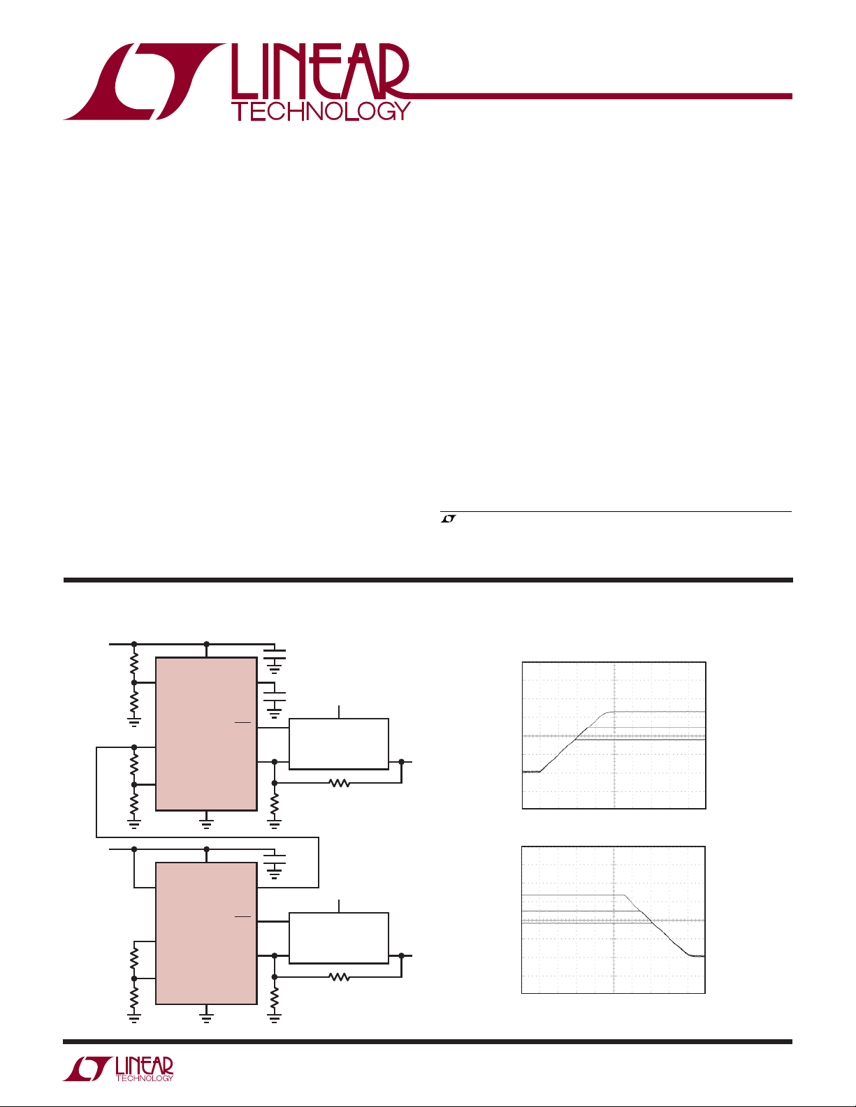
TYPICAL APPLICATIO
The LTC®2927 provides a simple solution to power supply
tracking and sequencing requirements. By selecting a few
resistors, the supply can be confi gured to ramp-up and
ramp-down with differing ramp rates, voltage offsets, or
time delays relative to other supplies or a master signal.
By forcing current into a feedback node of an independent
supply, the LTC2927 causes the output to track a ramp
signal without inserting any pass element losses. Because
the current is controlled in an open-loop manner, the
LTC2927 does not affect the transient response or stability of the supply. The compact solution at point of load
minimizes the trace length of the DC/DC circuit sensitive
FB node. Furthermore, it presents a high impedance when
power-up is complete, effectively removing it from the
DC/DC circuit.
, LT, LTC and LTM are registered trademarks of Linear Technology Corporation.
ThinSOT is a trademark of Linear Technology Corporation. All other trademarks are the
property of their respective owners. Patents Pending.
EARLY V
EARLY V
3.3V
3.3V
IN
IN
138k
100k
16.5k
13k
887k
412k
V
ON RAMP
RAMPBUF
TRACK
ON RAMP
RAMPBUF
TRACK
CC
LTC2927
GND
V
CC
LTC2927
GND
SDO RUN/SSFBIN
SDO RUN/SSFBIN
2927 TA01a
0.1μF
0.1μF
35.7k
0.1μF
412k
V
IN
DC/DC
FB = 1.235V OUT
16.5k
V
IN
DC/DC
FB = 0.8V OUT
887k
1.8V
2.5V
Track-Up and Track-Down Waveforms
1V/DIV
10ms/DIV
RAMP
(3.3V)
2.5V
1.8V
10ms/DIV
RAMP
(3.3V)
2.5V
1.8V
2927 TA01b
1V/DIV
2927 TA01c
2927fb
1
LTC2927
WW
W
ABSOLUTE AXI U RATI GS
U
(Note 1)
Supply Voltage (VCC) ................................. –0.3V to 10V
Input Voltages
ON ......................................................... –0.3V to 10V
TRACK .........................................–0.3V to V
+ 0.3V
CC
Output Voltages
FB, SDO ................................................. –0.3V to 10V
RAMP, RAMPBUF .........................–0.3V to V
+ 0.3V
CC
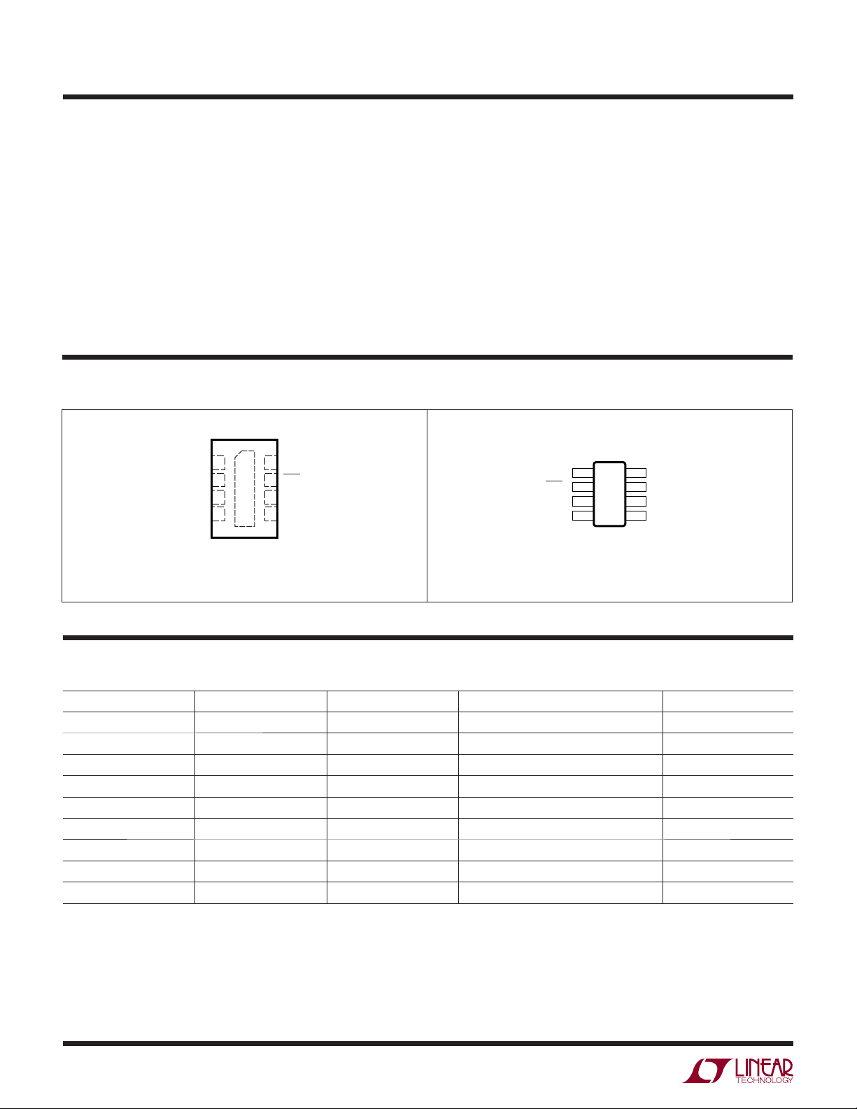
PIN CONFIGURATION
TOP VIEW
1ON
RAMP
2
RAMPBUF
8-LEAD (3mm × 2mm) PLASTIC DFN
EXPOSED PAD (PIN 9) PCB GND, CONNECTION OPTIONAL
3
TRACK
4
DDB PACKAGE
= 125°C, θJA = 76°C/W
T
JMAX
8
V
CC
SDO
7
9
FB
6
GND
5
Average Current
TRACK .................................................................5mA
FB ........................................................................5mA
RAMPBUF ............................................................5mA
Operating Temperature Range
LTC2927C ................................................ 0°C to 70°C
LTC2927I.............................................. –40°C to 85°C
Storage Temperature Range ...................–65°C to 150°C
Lead Temperature (Soldering, 10 sec) ..................300°C
TOP VIEW
VCC 1
SDO 2
FB 3
GND 4
TS8 PACKAGE
8-LEAD PLASTIC TSOT-23
T
= 125°C, θJA = 250°C/W
JMAX
8 ON
7 RAMP
6 RAMPBUF
5 TRACK
ORDER INFORMATION
LEAD FREE FINISH TAPE AND REEL PART MARKING* PACKAGE DESCRIPTION TEMPERATURE RANGE
LTC2927CDDB#PBF LTC2927CDDB#TRPBF LBQH
LTC2927IDDB#PBF LTC2927IDDB#TRPBF LBQH
LTC2927CTS8#PBF LTC2927CTS8#TRPBF LTBQJ 8-Lead Plastic TSOT-23 0°C to 70°C
LTC2927ITS8#PBF LTC2927ITS8#TRPBF LTBQJ 8-Lead Plastic TSOT-23 –40°C to 85°C
LEAD BASED FINISH TAPE AND REEL PART MARKING* PACKAGE DESCRIPTION TEMPERATURE RANGE
LTC2927CDDB LTC2927CDDB#TR LBQH
LTC2927IDDB LTC2927IDDB#TR LBQH
LTC2927CTS8 LTC2927CTS8#TR LTBQJ 8-Lead Plastic TSOT-23 0°C to 70°C
LTC2927ITS8 LTC2927ITS8#TR LTBQJ 8-Lead Plastic TSOT-23 –40°C to 85°C
Consult LTC Marketing for parts specifi ed with wider operating temperature ranges. *The temperature grade is identifi ed by a label on the shipping container.
For more information on lead free part marking, go to:
For more information on tape and reel specifi cations, go to:
http://www.linear.com/leadfree/
http://www.linear.com/tapeandreel/
8-Lead (3mm × 2mm) Plastic DFN
8-Lead (3mm × 2mm) Plastic DFN
8-Lead (3mm × 2mm) Plastic DFN
8-Lead (3mm × 2mm) Plastic DFN
0°C to 70°C
–40°C to 85°C
0°C to 70°C
–40°C to 85°C
2927fb
2
LTC2927
2
0
1
ELECTRICAL CHARACTERISTICS
The
temperature range, otherwise specifi cations are at T
= 25°C. 2.9V < VCC < 5.5V unless otherwise noted (Note 2).
A
l denotes the specifi cations which apply over the full operating
SYMBOL PARAMETER CONDITIONS MIN TYP MAX UNITS
V
CC
I
CC
V
CC(UVLO)
ΔV
CC(UVHYST)
V
ON(TH)
ΔV
ON(HYST)
I
ON
I
RAMP
V
RAMPBUF(OL)
V
RAMPBUF(OH)
V
OS
I
ERROR(%)
V
TRACK
I
FB(LEAK)
V
FB(CLAMP)
V
SDO(OL)
Supply Voltage
Supply Current IFB = 0mA, I
I
= –1mA, I
FB
TRACK
Supply Undervoltage Lockout VCC Rising
Supply Undervoltage Lockout Hysteresis 25 mV
ON Pin Threshold Voltage VON Rising
ON Pin Hysteresis
ON Pin Input Current VON = 1.2V, VCC = 5.5V
RAMP Pin Input Current 0V < V
0V < V
RAMPBUF Output Low Voltage I
RAMPBUF Output High Voltage,
V
RAMPBUF(OH)
= VCC – V
RAMPBUF
Ramp Buffer Offset,
V
= V
OS
IFB to I
TRACK
I
ERROR(%)
– V
RAMPBUF
Current Mismatch
= (IFB – I
TRACK
RAMP
)/I
TRACK
TRACK Pin Voltage I
RAMPBUF
I
RAMPBUF
V
RAMP
I
TRACK
I
TRACK
TRACK
I
TRACK
< VCC, Ramp On –9 –10 –11 μA
RAMP
< VCC, Ramp Off 9 10 11 μA
RAMP
= 1mA
= –1mA
= VCC/2, I
= –10μA
= –1mA
= –10μA
= –1mA
FB Pin Leakage Current VFB = 2V, VCC = 5.5V
FB Pin Clamp Voltage 1μA < IFB < 1mA
SDO Output Low Voltage I
= 1mA, VCC = 2.3V
SDO
Note 1: Stresses beyond those listed under Absolute Maximum Ratings
may cause permanent damage to the device. Exposure to any Absolute
Maximum Rating condition for extended periods may affect device
= 0mA
TRACK
RAMPBUF
= –1mA, I
= 0mA –30 0 30 mV
RAMPBUF
= –1mA
Note 2: All currents into the device pins are positive; all currents out of
device pins are negative. All voltages are referenced to ground unless
otherwise specifi ed.
l
2.9 5.5 V
l
0.25 0.56 1.2 mA
l
3 3.6 4.2 mA
l
2.2 2.5 2.7 V
l
1.210 1.230 1.250 V
l
30 75 150 mV
l
l
l
l
l
l
0.77 0.800 0.82 V
l
0.77 0.800 0.82 V
l
l
1.5 2 2.3 V
l
0 ±100 nA
20 100 mV
45 150 mV
0±5 %
0±5 %
±1 ±100 nA
0.1 0.4 V
reliability and lifetime.
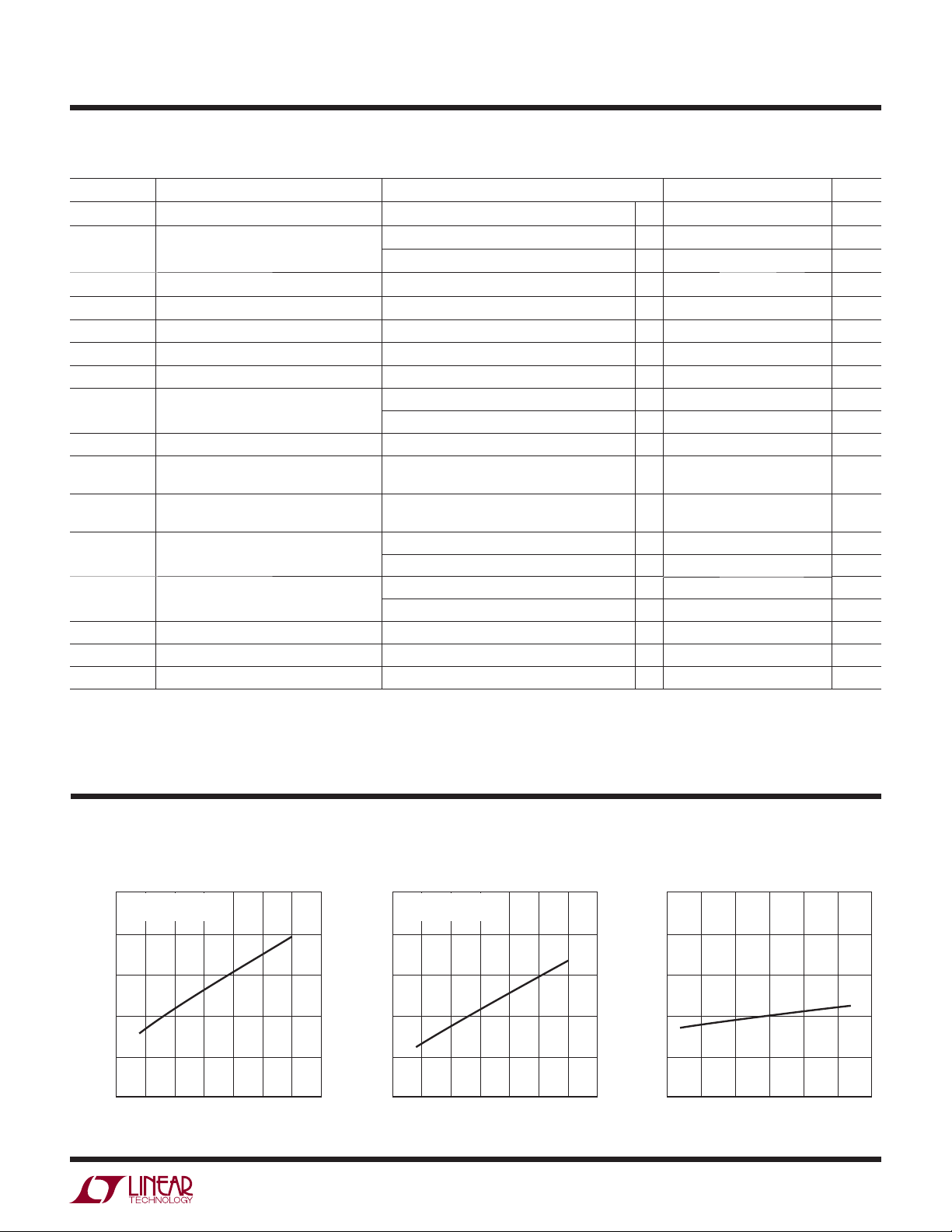
TYPICAL PERFORMANCE CHARACTERISTICS
750
700
650
(μA)
CC
I
600
550
500
ICC vs V
CC
I
= IFB = 0mA
TRACK
= 0mA
I
RAMBUF
3.0 3.5 4.0 4.5
2.5
VCC (V)
6.05.55.0
2927 G0
ICC vs V
I
TRACK
I
RAMBUF
CC
= IFB = –1mA
= –2mA
VCC (V)
4.70
4.65
4.60
(mA)
CC
I
4.55
4.50
4.45
2.5 3.0 3.5 4.0 4.5 6.
V
vs Temperature
TRACK
820
810
800
(mV)
TRACK
790
V
780
5.55.0
2927 G0
770
–25 0 25 50
–50
TEMPERATURE (°C)
75 100
2927 G03
2927fb
3
LTC2927
0
7
4
0
6
UW
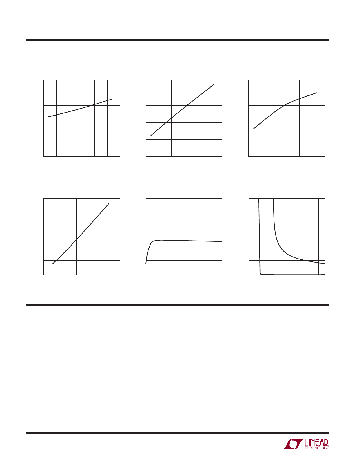
TYPICAL PERFOR A CE CHARACTERISTICS
1.240
1.235
1.230
(V)
1.225
ON(TH)
V
1.220
1.215
1.210
(mA)
I
60
50
40
TRACK
30
vs Temperature
ON(TH)
–25 0 25 50
–50
MAX I
V
TRACK
TEMPERATURE (°C)
TRACK
= 0V
vs V
CC
75 10
2927 G0
V
RAMPBUF(OL)
28
26
24
22
(mV)
20
18
RAMPBUF(OL)
16
V
14
12
10
–25 0 25 50
–50
TEMPERATURE (°C)
Tracking Cell Error vs I
5
ERROR = •
4
3
ERROR (%)
2
V
TRACK
0.8V
vs Temperature V
70
65
60
(mV)
55
RAMPBUF(OH)
50
V
45
40
1.0
0.8
0.6
(V)
SDO(OL)
0.4
V
I
I
TRACK
75 100
2927 G05
TRACK
FB
–1
RAMPBUF(OH)
–25 0 25 50
–50
V
SDO(OL)
TEMPERATURE (°C)
vs V
vs TemperatureV
CC
I
SDO
75 100
2927 G0
= 5mA
20
10
2.5 3.0 3.5 4.0 4.5 6.05.55.0
V
(V)
CC
PIN FUNCTIONS
2927 G0
TSOT/DFN Packages
1
0
1
234
I
TRACK
VCC (Pin 1/Pin 8): Supply Voltage Input. Operating range
is from 2.9V to 5.5V. An undervoltage lockout asserts SDO
until V
> 2.5V. VCC should be bypassed to GND with a
CC
0.1μF capacitor.
SDO (Pin 2/Pin 7): Slave Supply Shutdown Output. SDO
is an open-drain output that holds the shutdown (RUN/SS)
pin of the slave supply low until the V
pin is pulled above
CC
2.5V, and the ON pin is pulled above 1.23V, or RAMP is
above 200mV. SDO is pulled low again when both RAMP
< 200mV and ON < 1.23V. If the slave supply is capable
of operating with an input supply that is lower than the
LTC2927’s minimum operating voltage of 2.9V, the SDO
0.2
I
= 10μA
SDO
1234
VCC (V)
5
2927 G
(mA)
2927 G0
5
0.0
0
pin can be used to hold off the slave supply. Tie the SDO
pin to GND if unused.
FB (Pin 3/Pin 6): Feedback Control Output. FB pulls up
on the feedback node of the slave supply. Tracking is
achieved by mirroring the current from TRACK into FB.
A resistive divider connecting RAMPBUF and TRACK will
force the output voltage of the slave supply to track RAMP.
To prevent damage to the slave supply, the FB pin will not
force the slave’s feedback node above 2.3V. In addition,
the LTC2927 will not actively sink current from this node,
even when it is unpowered.
2927fb
4
UUU
PI FU CTIO S
LTC2927
TSOT/DFN Packages
GND (Pin 4/Pin 5): Device Ground.
TRACK (Pin 5/Pin 4): Tracking Control Input. A resistive
voltage divider between RAMPBUF and TRACK determines
the tracking profi le of the slave supply. TRACK servos to
0.8V, and the current supplied at TRACK is mirrored at FB.
The TRACK pin is capable of supplying at least 1mA when
= 2.9V. Under short circuit conditions, the TRACK pin
V
CC
is capable of supplying up to 70mA. Do not connect to
GND for extended periods. Limit the capacitance at the
TRACK pin to less than 25pF.
RAMPBUF (Pin 6/Pin 3): Ramp Buffer Output. Provides
a low impedance buffered version of the signal on the
RAMP pin. This buffered output drives the resistive voltage divider that connects to the TRACK pin. Limit the
capacitance at the RAMPBUF pin to less than 100pF. Float
RAMPBUF if unused.
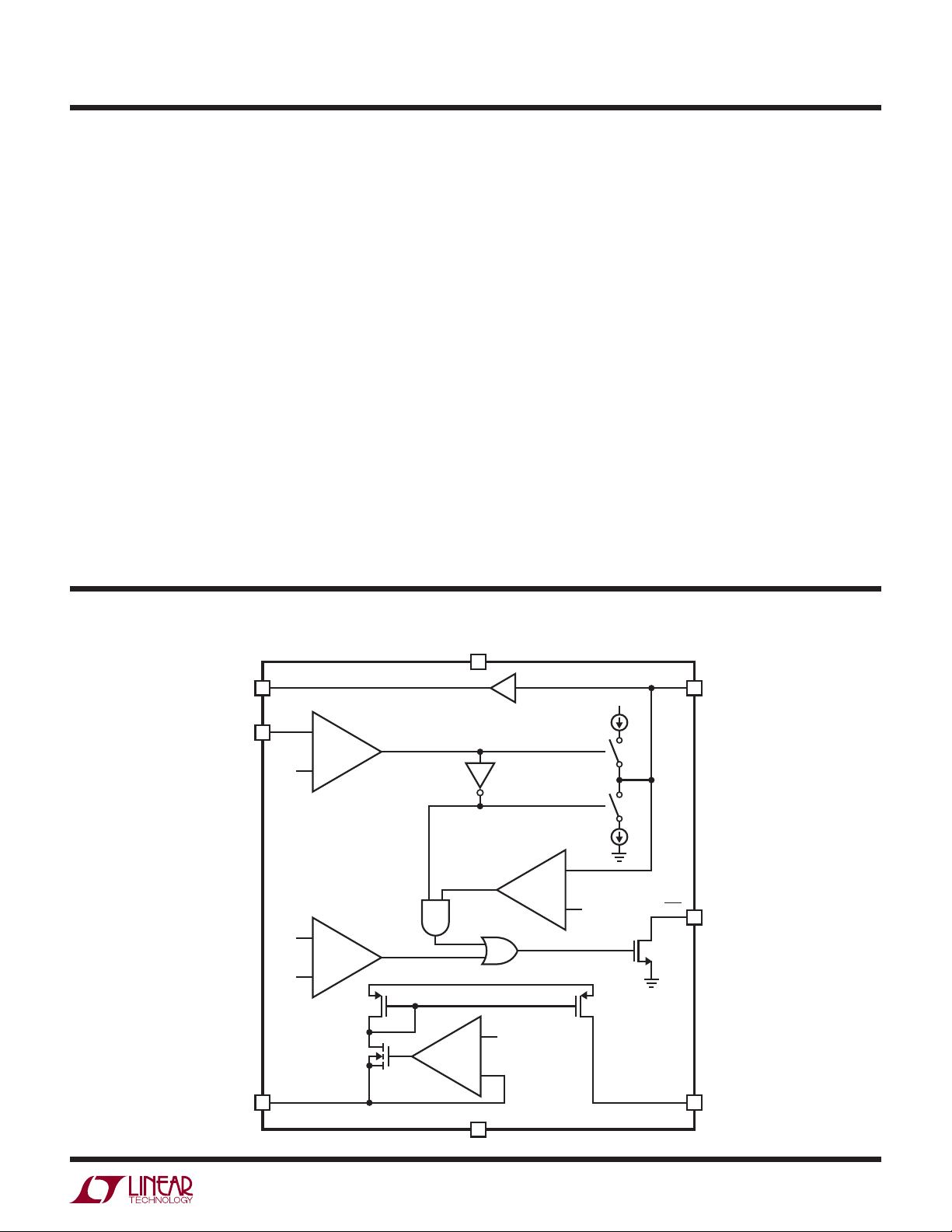
UU
W
FU CTIO AL BLOCK DIAGRA
RAMP (Pin 7/Pin 2): Ramp Buffer Input. The RAMP pin is
the input to the voltage buffer whose output drives a resistive voltage divider connected to the TRACK pin. Connect
this input to a capacitor to set the ramp voltage generated
from internal 10μA pull-up or pull-down currents. RAMP
can also be connected to an external ramping signal for
tracking. Ground RAMP if unused.
ON (Pin 8/Pin 1): On Control Input. The voltage level of
the ON pin relative to its 1.23V threshold (with 75mV
hysteresis) controls the tracking direction of the LTC2927.
An active high causes a 10μA pull-up current to fl ow at
the RAMP pin, which charges an external capacitor. An
active low at the ON pin causes a 10μA pull-down current at the RAMP pin to discharge the external capacitor
relative to GND.
Exposed Pad (NA/Pin 9): Exposed pad may be left open
or connected to device ground.
RAMPBUF
5
ON
5
1.23V
TRACK
5
2.5V
V
5
V
CC
1x
+
–
–
+
+
–
CC
UVLO
V
GND
CC
+
0.8V
–
5
V
10μA
10μA
0.2V
RAMP
SDO
FB
2927 BD
5
5
5
2927fb
CC
5

LTC2927
U
WUU
APPLICATIO S I FOR ATIO
Power Supply Tracking and Sequencing
The LTC2927 handles a variety of power-up profi les to
satisfy the requirements of digital logic circuits including
FPGAs, PLDs, DSPs and microprocessors. These requirements fall into one of the four general categories illustrated
in Figures 1 to 4.
Some applications require that the potential difference
between two power supplies must never exceed a specifi ed voltage. This requirement applies during power-up
and power-down as well as during steady-state operation,
often to prevent destructive latch-up in a dual supply
ASIC. Typically, this is achieved by ramping the supplies
up and down together (Figure 1). In other applications it
is desirable to have supplies ramp up and down with fi xed
voltage offsets between them (Figure 2) or to have them
ramp up and down ratiometrically (Figure 3).
Certain applications require one supply to come up after
another. For example, a system clock may need to start
before a block of logic. In this case, the supplies are sequenced as in Figure 4 where the 2.5V supply ramps up
after the 1.8V supply is completely powered.
Operation
The LTC2927 provides a simple solution to all of the
power supply tracking and sequencing profi les shown in
Figures 1 to 4. A single LTC2927 controls a single supply that tracks to a “master” signal. With two resistors,
a slave supply is confi gured to ramp up as a function of
the master signal. This master signal can be a separate
supply or it can be a ramp signal generated by tying the
RAMP pin to an external capacitor.
Tracking Cell
The LTC2927’s operation is based on the tracking cell
shown in Figure 5, which uses a proprietary wide-range
current mirror. The tracking cell shown in Figure 5 servos
the TRACK pin at 0.8V. The current supplied by the TRACK
1V/DIV
1V/DIV
10ms/DIV
Figure 1. Coincident Tracking
10ms/DIV
2927 F01
2927 F03
MASTER
SLAVE1
SLAVE2
MASTER
SLAVE1
SLAVE2
1V/DIV
1V/DIV
10ms/DIV
Figure 2. Offset Tracking
10ms/DIV
MASTER
SLAVE1
SLAVE2
2927 F02
MASTER
SLAVE1
SLAVE2
2927 F04
6
Figure 3. Ratiometric Tracking
Figure 4. Supply Sequencing
2927fb

LTC2927
U
WUU
APPLICATIO S I FOR ATIO
pin is mirrored at the FB pin to establish a voltage at the
output of the slave supply. The slave output voltage varies
with the master signal, enabling the slave supply to be
controlled as a function of the master signal with terms
set by R
and RTB, it is possible to generate any of the profi les
R
TA
in Figures 1 to 4.
Controlling the Ramp-Up and Ramp-Down Behavior
The operation of the LTC2927 is most easily understood
by referring to the simplifi ed functional diagram in Figure
6. When the ON pin is low, the master signal at the RAMP
pin is pulled to ground. Since the current through R
at its maximum when the master signal is low, the current
from FB is also at its maximum. This current drives the
slave output to its minimum voltage.
When the ON pin rises above 1.23V, the master signal
rises and the slave supply tracks the master signal. The
ramp rate is set by an external capacitor driven by a 10μA
current source at the RAMP pin. Alternatively, the RAMP
pin can be connected to a separate supply to be used as
the master signal.
In a properly designed system, when the master signal
has reached its maximum voltage the current from the
TRACK pin is zero. In this case, there is no current from
the FB pin and the LTC2927 has no effect on the output
voltage accuracy, transient response or stability of the
slave supply.
When the ON pin falls below V
cally 1.225V, the RAMP pin pulls down with 10μA and the
master signal and slave supplies will fall at the same rate
as they rose previously.
and RTB. By selecting appropriate values of
TA
TB
– ΔV
ON(TH)
V
CC
ON(HYST)
, typi-
is
The ON pin can be controlled by a digital I/O pin or it
can be used to monitor an input supply. By connecting a
resistive divider from an input supply to the ON pin, the
supplies will ramp up only after the monitored supply has
reached a preset voltage.
If a resistive divider is used to set the ON pin voltage, choose
values that will keep this voltage above the maximum ON
pin threshold voltage of 1.25V at the lowest operating
supply level.
The Ramp Buffer
The RAMPBUF pin provides a buffered version of the
RAMP pin voltage that drives the resistive divider on the
TRACK pin. The buffered master signal provides up to
2mA to drive the resistors.
Shutdown Output
In some applications it might be necessary to control
the shutdown or RUN/SS pins of the slave supplies. The
LTC2927 may not be able to supply the rated 1mA of current
from the FB pin when V
is below 2.9V. If the slave power
CC
supply is capable of operating at low input voltages, use
the open-drain SDO output to drive the SHDN or RUN/SS
pin of the slave supply (see Figure 7). This will hold the
slave supply output low until the ON pin is above 1.23V
and V
R
R
is above the 2.5V undervoltage lockout condition.
CC
V
CC
5
ONB
ONA
5
5
ON
1.2V
RAMPBUF
+
–
1x
V
CC
10μA
10μA
RAMP
5
C
MASTER
RAMP
MASTER
R
TB
R
TA
+
+
+
0.8V
–
–
TRACK
5
FB
2927 F05
DC/DC
5
FB OUT
R
FB
R
FA
SLAVE
R
TB
TRACK
5
R
TA
0.8V
–
FB
5
DC/DC
R
5
2927 F06
FB
R
FA
SLAVE
Figure 6. Simplifi ed Functional DiagramFigure 5. Simplifi ed Tracking Cell
2927fb
7

LTC2927
U
WUU
APPLICATIO S I FOR ATIO
EARLY
V
IN
3.3V
R
ONB
138k
R
ONA
100k
R
TB
16.5k
R
TA
13k
SDO pulls low again when the ON pin is pulled below 1.23V
and the RAMP pin is below about 200mV.
3-Step Design Procedure
The following 3-step procedure allows one to complete
a design for any of the tracking or sequencing profi les
shown in Figures 1 to 4. A basic single supply application
circuit is shown in Figure 8.
1. Set the ramp rate of the master signal.
Solve for the value of C
pin, based on the desired ramp rate (V/s) of the master
supply, S
0.1μF
V
CC
ON RAMP MASTER
LTC2927
SDO
RAMPBUF
TRACK
GND
FB
2927 F07
C
RAMP
V
10pF
IN
RUN/SS IN
DC/DC
FB = 1.235V OUT
R
16.5k
FB
R
FA
35.7k
Figure 7. SDO Shutdown Application
, the capacitor on the RAMP
RAMP
.
M
1.8V
Choose a ramp rate for the slave supply, S
. If the slave
S
supply ramps up coincident with the master signal or
with a fi xed voltage offset, then the ramp rate equals
the master supply’s ramp rate. Be sure to use a fast
enough ramp rate for the slave supply so that it will fi nish
ramping before the master signal has reached its fi nal
supply value. If not, the slave supply will be held below
the intended regulation value by the master signal. Use
the following formulas to determine the resistor values
for the desired ramp rate, where R
feedback resistors in the slave supply and V
and RFA are the
FB
is the
FB
feedback reference voltage of the slave supply:
S
RR
=• ()2
TB FB
′
R
=
TA
where V
TRACK
M
S
S
V
FB
+−
R
FB
R
≈ 0.8V.
V
TRACK
V
FB
FA
V
TRACK
R
TB
Note that large ratios of slave ramp rate to master ramp
rate, S
suffi ciently large delay is used in step 3, R
positive, otherwise S
3. Choose R
, may result in negative values for RTA’. If
S/SM
must be reduced.
S/SM
to obtain the desired delay.
TA
will be
TA
()3
I
C
RAMP
RAMP
=≈μ10 1()
where I A
S
M
RAMP
2. Solve for the pair of resistors that provide the desired
ramp rate of the slave supply, assuming no delay.
EARLY
V
IN
R
ONB
R
ONA
R
TB
R
TA
0.1μF
V
CC
ON RAMP MASTER
LTC2927
RAMPBUF
TRACK
GND
2927 F08
C
RAMP
V
IN
IN
FB
DC/DC
FB OUT
R
R
FB
FA
SLAVE
Figure 8. Single Supply Application
8
If no delay is required, such as in coincident and ratiometric tracking, then simply set R
= RTA’. If a delay
TA
is desired, as in offset tracking and supply sequencing,
calculate R
” to determine the value of RTA where tD
TA
is the desired delay in seconds.
VR
″
R
=
TA
=
RRR
TA TA TA
•
TRACK TB
tS
•
DM
′″
|| ( )5
()4
the parallel combination of RTA’ and RTA”.
As noted in step 2, small delays and large ratios of slave ramp
rate to master ramp rate (usually only seen in sequencing)
may result in solutions with negative values for R
. In such
TA
cases, either the delay must be increased or the ratio of
slave ramp rate to master ramp rate must be reduced.
2927fb

LTC2927
U
WUU
APPLICATIO S I FOR ATIO
Coincident Tracking Example
MASTER
1V/DIV
10ms/DIV
Figure 9. Coincident Tracking (from Figure 10)
A typical application is shown in Figure 10. The master
signal is a 3.3V ramp generated by the LTC2927. The
slave 1 supply is a 1.8V switching power supply and the
slave 2 supply is a 2.5V switching power supply. Both
slave supplies track coincidently with the 3.3V ramping
master signal. The ramp rate of the supplies is 100V/s.
The 3-step design procedure detailed previously can be
used to determine component values. Only the slave 1
supply is considered here as the procedure is the same
for the slave 2 supply.
1. Set the ramp rate of the master signal.
From Equation 1:
A
10
C
RAMP
μ
==μ
Vs
100
/
01
.
F
2. Solve for the pair of resistors that provide the desired
slave supply behavior, assuming no delay.
From Equation 2:
SLAVE2
SLAVE1
1V/DIV
10ms/DIV
2927 F09
In this example, the supply remains low while the ON pin
is held below 1.23V. When the ON pin rises above 1.23V,
10μA pulls up the master signal on C
at 100V/s.
RAMP
The master signal is buffered from the RAMP pin to the
RAMPBUF pin. As this output and the RAMPBUF pin rise,
the current from the TRACK pin is reduced. Consequently,
the voltage at the slave supply’s output is increased, and
the slave supply tracks the master signal. When the ON
pin is again pulled below 1.23V, 10μA will pull down C
RAMP
at 100V/s. If the loads on the outputs are suffi cient, all
outputs will track down coincidently at 100V/s.
EARLY V
IN
3.3V
R
ONB
138k
R
ONA
100k
R
16.5k
R
13k
TB1
TA1
V
CC
ON RAMP
LTC2927
SDO RUN/SSFBIN
RAMPBUF
TRACK
GND
0.1μF
0.1μF
3.3V
DC/DC
FB = 1.235V OUT
R
R
FA1
35.7k
FB1
16.5k
MASTER
3.3V
SLAVE1
1.8V
Vs
100
Rk
=• =16 5
TB
100
/
Vs
/
k
16 5.
.ΩΩ
From Equation 3:
V
08
′
R
=
TA
1 235
.
16 5
.
V
k
.
V
1 235
.
+−
35 7
.
k
08
.
16 5
.ΩΩΩ
3. Choose RTA to obtain desired delay.
Since no delay is desired, R
= RTA’
TA
EARLY
3.3V
V
CC
ON RAMP
LTC2927
k
≈
13
V
k
Ω
R
TB2
887k
R
TA2
412k
RAMPBUF
TRACK
SDO RUN/SSFBIN
GND
2927 F10
0.1μF
3.3V
DC/DC
FB = 0.8V OUT
R
R
FA2
412k
FB2
887k
SLAVE2
2.5V
Figure 10. Coincident Tracking Example
2927fb
9

LTC2927
U
WUU
APPLICATIO S I FOR ATIO
Ratiometric Tracking Example
MASTER
CC
SLAVE2
SLAVE1
=
1V/DIV
10ms/DIV
Figure 11. Ratiometric Tracking (from Figure 12)
This example converts the coincident tracking example to
the ratiometric tracking profi le shown in Figure 11. The
ramp rate of the master signal remains unchanged (Step
1) and there is no delay in ratiometric tracking (Step 3),
so only the result of step 2 in the 3-step design procedure
needs to be considered. In this example, the ramp rate of the
1.8V slave 1 supply ramps up at 60V/s and the 2.5V slave 2
supply ramps up at 85V/s. Always verify that the chosen
ramp rate will allow the supplies to ramp-up completely
before RAMPBUF reaches V
. If the 1.8V supply were
CC
to ramp-up at 50V/s it would only reach 1.65V because
the RAMPBUF signal would reach its fi nal value of V
3.3V before the slave supply reached 1.8V.
2. Solve for the pair of resistors that provide the desired
slave supply behavior, assuming no delay.
From Equation 2:
Vs
100
Rk
=• =16 5
TB
60
/
Vs
/
k
27 4.
.ΩΩ
From Equation 3:
EARLY V
EARLY
3.3V
3.3V
10ms/DIV
IN
R
ONB
138k
R
ONA
100k
R
27.4k
R
10k
R
R
383k
TB1
TA1
TB2
1M
TA2
V
CC
ON RAMP
LTC2927
SDO RUN/SSFBIN
RAMPBUF
TRACK
GND
V
CC
ON RAMP
LTC2927
SDO RUN/SSFBIN
RAMPBUF
TRACK
GND
2927 F12
R
35.7k
R
412k
Figure 12. Ratiometric Tracking Example
1V/DIV
2927 F11
0.1μF
0.1μF
3.3V
DC/DC
FB = 1.235V OUT
R
FB1
FA1
16.5k
0.1μF
3.3V
DC/DC
FB = 0.8V OUT
R
FB2
FA2
887k
MASTER
3.3V
SLAVE1
1.8V
SLAVE2
2.5V
V
08
′
R
=
TA
1 235
.
16 5
.
V
k
.
+−
35 7
.
k
V
1 235
.
V
08
.
k
27 4
.ΩΩΩ
k
≈
10
Ω
Step 3 is unnecessary because there is no delay, so
= RTA’
R
TA
10
2927fb

LTC2927
U
WUU
APPLICATIO S I FOR ATIO
Offset Tracking Example
MASTER
1V/DIV
10ms/DIV
Figure 13. Offset Tracking (from Figure 14)
Converting the circuit in the coincident tracking example
to the offset tracking shown in Figure 13 is relatively
simple. Here the 1.8V slave 1 supply ramps up 1V below
the master. The ramp rate remains the same (100V/s), so
there are no changes necessary to steps 1 and 2 of the
3-step design procedure. Only step 3 must be considered.
Be sure to verify that the chosen voltage offset will allow
the slave supply to ramp up completely. In this example,
if the voltage offset were 2V, the slave supply would only
ramp to 3.3V – 2V = 1.3V.
3. Choose R
First, convert the desired voltage offset, V
, using the ramp rate:
t
D
t
== =
D
to obtain desired delay.
TA
V
100
1
Vs
V
OS
S
, to a delay
OS
ms
10 6/()
From Equation 4:
SLAVE2
SLAVE1
EARLY V
EARLY
3.3V
3.3V
1V/DIV
10ms/DIV
IN
R
ONB
138k
R
ONA
100k
R
16.5k
R
6.65k
R
887k
R
316k
TB1
TA1
TB2
TA2
V
CC
ON RAMP
LTC2927
SDO RUN/SSFBIN
RAMPBUF
TRACK
GND
V
CC
ON RAMP
LTC2927
SDO RUN/SSFBIN
RAMPBUF
TRACK
GND
2927 F14
2927 F13
0.1μF
0.1μF
3.3V
DC/DC
FB = 1.235V OUT
R
R
35.7k
R
412k
FB1
FA1
16.5k
0.1μF
3.3V
DC/DC
FB = 0.8V OUT
R
FB2
FA2
887k
MASTER
3.3V
SLAVE1
1.8V
SLAVE2
2.5V
R
=
TA
ms V s
•
10 100
/
=
13 2
.ΩΩ
k
Vk
•
0 8 16 5
..
″
From Equation 5:
Rkkk
=≈131 132 665.. .ΩΩ Ω
TA
Figure 14. Offset Tracking Example
2927fb
11

LTC2927
U
WUU
APPLICATIO S I FOR ATIO
Supply Sequencing Example
MASTER
1V/DIV
10ms/DIV
Figure 15. Supply Sequencing (from Figure 16)
In Figure 15, the slave 1 supply and the slave 2 supply are
sequenced instead of tracking. The 3.3V master ramps up
at 100V/s. The 1.8V slave 1 supply ramps up at 1000V/s
beginning 10ms after the master signal starts to ramp up.
The 2.5V slave 2 supply ramps up at 1000V/s beginning
25ms after the master signal begins to ramp up. Note
that not every combination of ramp rates and delays is
possible. Small delays and large ratios of slave ramp rate
to master ramp rate may result in solutions that require
negative resistors. In such cases, either the delay must
be increased or the ratio of slave ramp rate to master
ramp rate must be reduced. In this example, solving for
the slave supply yields:
1. Set the ramp rate of the master signal.
From Equation 1:
A
10
C
RAMP
μ
==μ
Vs
100
/
01
.
F
SLAVE2
SLAVE1
1V/DIV
10ms/DIV
2927 F15
3. Choose RTA to obtain desired delay.
From Equation 4:
R
=
TA
ms V s
•
10 100
/
=
132
.ΩΩ
k
Vk
•
08 165
..
″
From Equation 5:
Rkkk
=− =213 132 348.. .ΩΩ Ω
TA
EARLY V
IN
3.3V
R
ONB
138k
R
ONA
100k
R
1.65k
R
3.48k
TB1
TA1
V
CC
ON RAMP
LTC2927
SDO RUN/SSFBIN
RAMPBUF
TRACK
GND
0.1μF
0.1μF
3.3V
DC/DC
FB = 1.235V OUT
R
35.7k
R
FA1
16.5k
FB1
MASTER
3.3V
SLAVE1
1.8V
2. Solve for the pair of resistors that provide the desired
slave supply behavior, assuming no delay.
Vs
100
Rk
=• =16 5
TB
1000
/
Vs
/
k
165.
.ΩΩ
From Equation 3:
V
08
′
R
=
TA
V
1 235
.
k
16 5
.
ΩΩΩ
.
+−
35 7
.
k
V
1 235
.
08
.
165
.
V
k
=−
213
.
k
Ω
12
EARLY
3.3V
0.1μF
FB = 0.8V OUT
R
FA2
412k
R
88.7k
R
36.5k
TB2
TA2
V
CC
ON RAMP
LTC2927
SDO RUN/SSFBIN
RAMPBUF
TRACK
GND
2927 F16
Figure 16. Supply Sequencing Example
3.3V
DC/DC
R
FB2
887k
SLAVE2
2.5V
2927fb

LTC2927
U
WUU
APPLICATIO S I FOR ATIO
Final Sanity Checks
The collection of equations below is useful for identifying
unrealizable solutions.
As stated in step 2, the slave supply must fi nish ramping
before the master signal has reached its fi nal voltage. This
can be verifi ed by the following equation:
TRACK
TRACK
⎛
1+
⎜
⎝
V
Here, V
master signal (VCC if RAMP pin).
It is possible to choose resistor values that require the
LTC2927 to supply more current than the Electrical Characteristics table guarantees. To avoid this condition, check
that I
does not exceed 1mA and I
TRACK
exceed ±2mA.
To confi rm that I
guaranteed current, verify that:
V
TRACK
RR
TA TB
Finally, check that the RAMPBUF pin will not be forced to
sink more than 2mA when it is at 0V or be forced to source
more than 2mA when it is at V
V
TRACK
R
<
TB
⎞
R
TB
⎟
⎠
R
TA
= 0.8V. V
TRACK
mA
< 1
mA and
V
<
MASTER
MASTER
is the fi nal voltage of the
RAMPBUF
does not
< 1mA, the TRACK pin’s maximum
MASTER
V
MASTER
RR
+
TA TB
.
mA
<22
R
ONB
R
ONA
<
29
.
121
.
V
1
–
V
For example, if the typical application shown on page 1
has a 3.3V ±10% V
, the lowest possible operating supply
IN
voltage will be 2.97.
If R
R
ONB
>=
R
ONA
is 100k then R
ONA
297
.
125
.
V
1 1 376
–.
V
ONB
must be greater than 137.6k.
Therefore, 138k is chosen. These values must be checked
to ensure the supply reaches the LTC2927 minimum operating supply voltage of 2.9V before the ON pin is above
the minimum threshold.
29
.
138
121
.
V
V
1 1 389.
–.<=
Load Requirements
When the supply is ramped down quickly, either the load
or the supply itself must be capable of sinking enough
current to support the ramp rate. For example, if there
is a large output capacitance on the supply and a weak
resistive load, supplies that do not sink current will have
their falling ramp rate limited by the RC time constant of
the load and the output capacitance. Figure 17 shows the
case when the slave supply does not track the master
near ground.
ON Pin Resistive Divider
Check that the ON pin voltage is above the 1.25V maximum
threshold at the lowest possible supply voltage value.
<
V
CC MIN
()
.–125
1
V
R
ONB
R
ONA
Also check that the supply voltage is above the minimum
LTC2927 operating supply voltage of 2.9V before the ON
pin is above the 1.21V minimum threshold voltage.
MASTER
SLAVE
10ms/DIV
Figure 17. Weak Resistive Load
1V/DIV
2927 F17
2927fb
13

LTC2927
U
WUU
APPLICATIO S I FOR ATIO
Start-Up Delays
Often power supplies do not start-up immediately when
their input supplies are applied. If the LTC2927 tries to
ramp-up these power supplies as soon as the input supply is present, the start-up of the outputs may be delayed,
defeating the tracking circuit (Figure 18). Often this delay is
intentionally confi gured by a soft-start capacitor. This can
be remedied either by reducing the soft-start capacitor on
the slave supply or by including a capacitor in the ON pin’s
resistive divider to delay the ramp up. See Figure 19.
MASTER
1V/DIV
20ms/DIV
SLAVE
ON
2927 F18
Layout Considerations
Be sure to place a 0.1μF bypass capacitor as near as possible to the supply pin of the LTC2927.
To minimize the noise on the slave supply’s output, keep
the trace connecting the FB pin of the LTC2927 and the
feedback node of the slave supply as short as possible.
In addition, do not route this trace next to signals with
fast transition times. In some circumstances it might be
advantageous to add a resistor near the feedback node of
the slave supply in series with the FB pin of the LTC2927.
This resistor must not exceed:
R
SERIES
15 15
..
VV
=
−
I
MAX FB
⎛
FB
=−
⎜
V
⎝
⎞
V
1
RR
()
⎟
FA FB
⎠
This resistor is most effective if there is already a capacitor at the feedback node of the slave supply (often a
compensation component). Increasing the capacitance on
a slave supply’s feedback node will further improve the
noise immunity, but could affect the stability and transient
response of the supply.
Figure 18. Power Supply Start-Up Delayed
1V/DIV
5ms/DIV
Figure 19. ON Pin Delayed
2927 F19
MASTER
SLAVE
ON
V
CC
R
LTC2927
0.1μF
Figure 20. Layout Considerations
GND
FB
MINIMIZE
2927 F20
SERIES
TRACE
LENGTH
FB OUT
R
FA
DC/DC
R
FB
14
2927fb

PACKAGE DESCRIPTIO
LTC2927
U
DDB Package
8-Lead Plastic DFN (3mm × 2mm)
(Reference LTC DWG # 05-08-1702)
0.61 ±0.05
(2 SIDES)
0.675 ±0.05
2.50 ±0.05
1.15 ±0.05
PACKAGE
0.25 ± 0.05
RECOMMENDED SOLDER PAD PITCH AND DIMENSIONS
NOTE:
1. DRAWING CONFORMS TO VERSION (WECD-1) IN JEDEC PACKAGE OUTLINE M0-229
2. DRAWING NOT TO SCALE
3. ALL DIMENSIONS ARE IN MILLIMETERS
4. DIMENSIONS OF EXPOSED PAD ON BOTTOM OF PACKAGE DO NOT INCLUDE
MOLD FLASH. MOLD FLASH, IF PRESENT, SHALL NOT EXCEED 0.15mm ON ANY SIDE
5. EXPOSED PAD SHALL BE SOLDER PLATED
6. SHADED AREA IS ONLY A REFERENCE FOR PIN 1 LOCATION ON THE TOP AND BOTTOM OF PACKAGE
2.20 ±0.05
(2 SIDES)
0.50 BSC
OUTLINE
PIN 1 BAR
TOP MARK
(SEE NOTE 6)
0.200 REF
3.00 ±0.10
(2 SIDES)
TS8 Package
8-Lead Plastic TSOT-23
(Reference LTC DWG # 05-08-1637)
0.52
MAX
0.65
REF
2.00 ±0.10
(2 SIDES)
0.75 ±0.05
0 – 0.05
R = 0.115
0.56 ± 0.05
(2 SIDES)
2.90 BSC
(NOTE 4)
TYP
0.25 ± 0.05
BOTTOM VIEW—EXPOSED PAD
2.15 ±0.05
(2 SIDES)
0.38 ± 0.10
85
14
0.50 BSC
PIN 1
CHAMFER OF
EXPOSED PAD
(DDB8) DFN 1103
3.85 MAX
2.62 REF
RECOMMENDED SOLDER PAD LAYOUT
PER IPC CALCULATOR
0.20 BSC
DATUM ‘A’
0.30 – 0.50 REF
NOTE:
1. DIMENSIONS ARE IN MILLIMETERS
2. DRAWING NOT TO SCALE
3. DIMENSIONS ARE INCLUSIVE OF PLATING
4. DIMENSIONS ARE EXCLUSIVE OF MOLD FLASH AND METAL BURR
5. MOLD FLASH SHALL NOT EXCEED 0.254mm
6. JEDEC PACKAGE REFERENCE IS MO-193
Information furnished by Linear Technology Corporation is believed to be accurate and reliable.
no responsibility is assumed for its use. Linear Technology Corporation makes no representation that
the interconnection of its circuits as described herein will not infringe on existing patent rights.
1.22 REF
1.4 MIN
2.80 BSC
0.09 – 0.20
(NOTE 3)
1.50 – 1.75
(NOTE 4)
1.00 MAX
0.65 BSC
0.80 – 0.90
PIN ONE ID
1.95 BSC
However,
0.22 – 0.36
8 PLCS (NOTE 3)
0.01 – 0.10
TS8 TSOT-23 0802
2927fb
15

LTC2927
TYPICAL APPLICATIO
U
High Voltage Supply ApplicationSingle Supply Application
EARLY
V
3.3V
IN
R
ONB
138k
R
ONA
100k
R
16.5k
R
13k
0.1μF
V
ON RAMP MASTER
RAMPBUF
TB
TRACK
TA
CC
LTC2927
GND
SDO
FB
2927 TA02a
R
35.7k
C
RAMP
0.1μF
3.3V
RUN/SS IN
DC/DC
FB = 1.235V OUT
R
FA
FB
16.5k
1.8V
EARLY
V
3.3V
IN
R
ONB
138k
R
ONA
100k
R
78.7k
R
28k
0.1μF
V
ON RAMP MASTER
RAMPBUF
TB
TRACK
TA
CC
LTC2927
GND
SDO
FB
2927 TA02b
R
35.7k
C
RAMP
0.4μF
3.3V
RUN/SS IN
DC/DC
FB = 1.235V OUT
R
311k
FB
FA
SLAVE
12V
RELATED PARTS
PART NUMBER DESCRIPTION COMMENTS
LTC2920 Power Supply Margining Controller Single or Dual Versions, Symmetric as Symmetric High and Low Margining
LTC2921/LTC2922 Power Supply Tracker with Input Monitors Includes 3 (LTC2921) or 5 (LTC2922) Remote Sense Switches
LTC2923 Power Supply Tracking Controller Controls 3 Supplies for Tracking or Sequencing
LTC2924 Quad Power Supply Sequencer Controls 4 Supplies for Sequencing
LTC2925 Multiple Power Supply Tracking Controller with
Power Good Timeout
LTC2926 MOSFET-Controlled Power Supply Tracker Active Tracking Control with Series MOSFETs
LTC2928 Multichannel Power Supply Sequencer
and Supervisor
™
LT4220 Dual Supply Hot Swap
Controller ±2.7V to ±16.5V, Supply Tracking Mode
LTC4221 Dual Hot Swap Controller Operates from 1V to 13.5V, Allows Supply Sequencing, Active Current Limiting
LTC4230 Triple Hot Swap Controller with Multifunction
Current Control
LTC4253 –48V Hot Swap Controller and Supply
Sequencer
Hot Swap is a trademark of Linear Technology Corporation.
Controls 4 Supplies for Tracking or Sequencing
Programmable with External Components; No Software Required
1.7V to 16.5V, Active Inrush Limiting, Fast Comparator
Floating Supply from –15V, Active Current Limiting, Enables Three DC/DC
Converters
16
Linear Technology Corporation
1630 McCarthy Blvd., Milpitas, CA 95035-7417
(408) 432-1900 ● FAX: (408) 434-0507
●
www.linear.com
2927fb
LT 0308 REV B • PRINTED IN USA
© LINEAR TECHNOLOGY CORPORATION 2006
 Loading...