

Page 1
advertisement
Power Supply Tracker Can Also Margin Supplies – Design Note 372
Dan Eddleman
Power supply margining is a technique commonly used to
test circuit boards in production. By adjusting power
supply output voltages, electrical components are tested
at the upper and lower supply voltage limits specified for
a design. The LTC
®
2923 power supply tracking controller
can be used to margin supplies in addition to its usual task
of tracking multiple power supplies.
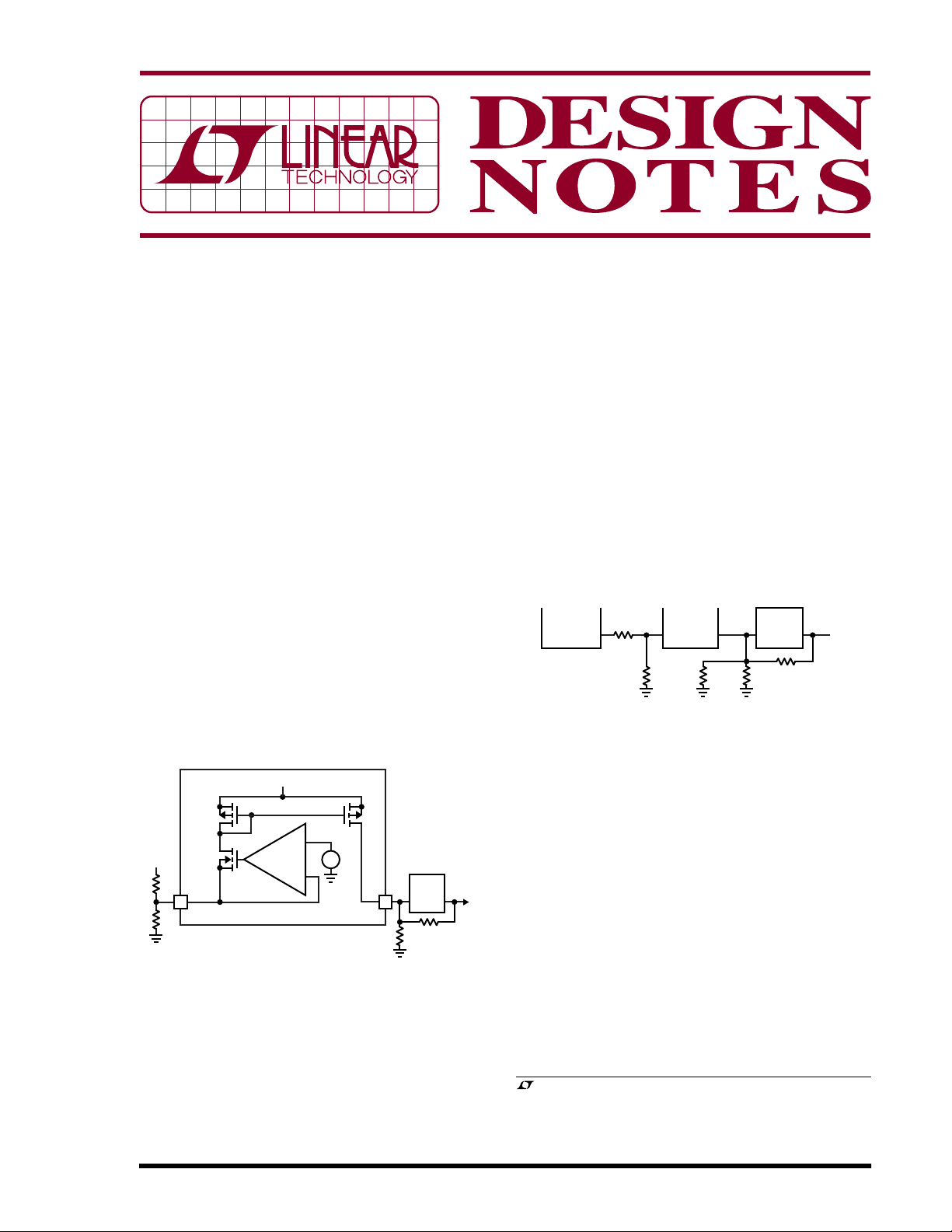
The LTC2923 uses the simple tracking cell shown in
Figure 1 to control the ramp-up and ramp-down behavior
of multiple supplies. This cell servos the TRACK input to
0.8V and mirrors the current supplied by that pin at the FB
output pin. The FB pin connects to the feedback node of
the slave power supply. Normally, a resistive divider
connects the master signal to the TRACK pin. By selecting
the appropriate resistor values, R
and RTB, the relation-
TA
ship of the slave power supply is configured relative to the
master signal.
The supply margining application uses an LTC2923 tracking cell to margin a supply high and low under the control
of a three-state I/O pin.
V
CC
+
+
MASTER
R
TB
TRACK
R
TA
0.8V
–
–
FB
FB OUT
R
FA
DN372 F01
DC/DC
R
SLAVE
FB
Figure 1. Simplified Tracking Cell
In the circuit shown in Figure 2, the supply is margined to
its high, low and nominal output voltages by driving the
I/O pin to its high, low and high impedance states
respectively. This example shows calculated resistor
values rather than standard resistor values for ease of
illustration. If the feedback voltage, VFB, of the power
supply is 0.8V, solve for the value of R
added in parallel with R
of the existing design to
F1
that must be
FM1
produce the desired high margin output.
In Figure 2, the feedback resistors RF2 and RF1 produce an
output voltage of 2.5V. To margin 10% high to 2.75V
requires a 54.4k resistor, R
connect a resistor, R
TM1
, in parallel with RF1. Now
FM1
, whose value is equal to R
FM1
between the TRACK pin and ground. If the output will be
margined low by the same voltage that it was margined
high, then connect another resistor, R
, equal to R
TM2
FM1
,
between the TRACK pin and the three-state I/O pin.
R
THREE-STATE
TM2
54.4k
I/O
R
TM1
54.4k
LTC2923
TRACK2
FB2
R
FM1
54.4k
DC/DC
V
= 0.8V
FB
R
R
F2
F1
17k
8k
DN372 F02
V
OUT
Figure 2. The LTC2923 Margins the Output of a 2.5V
Supply 10% High or Low Under the Control of a
Three-State I/O
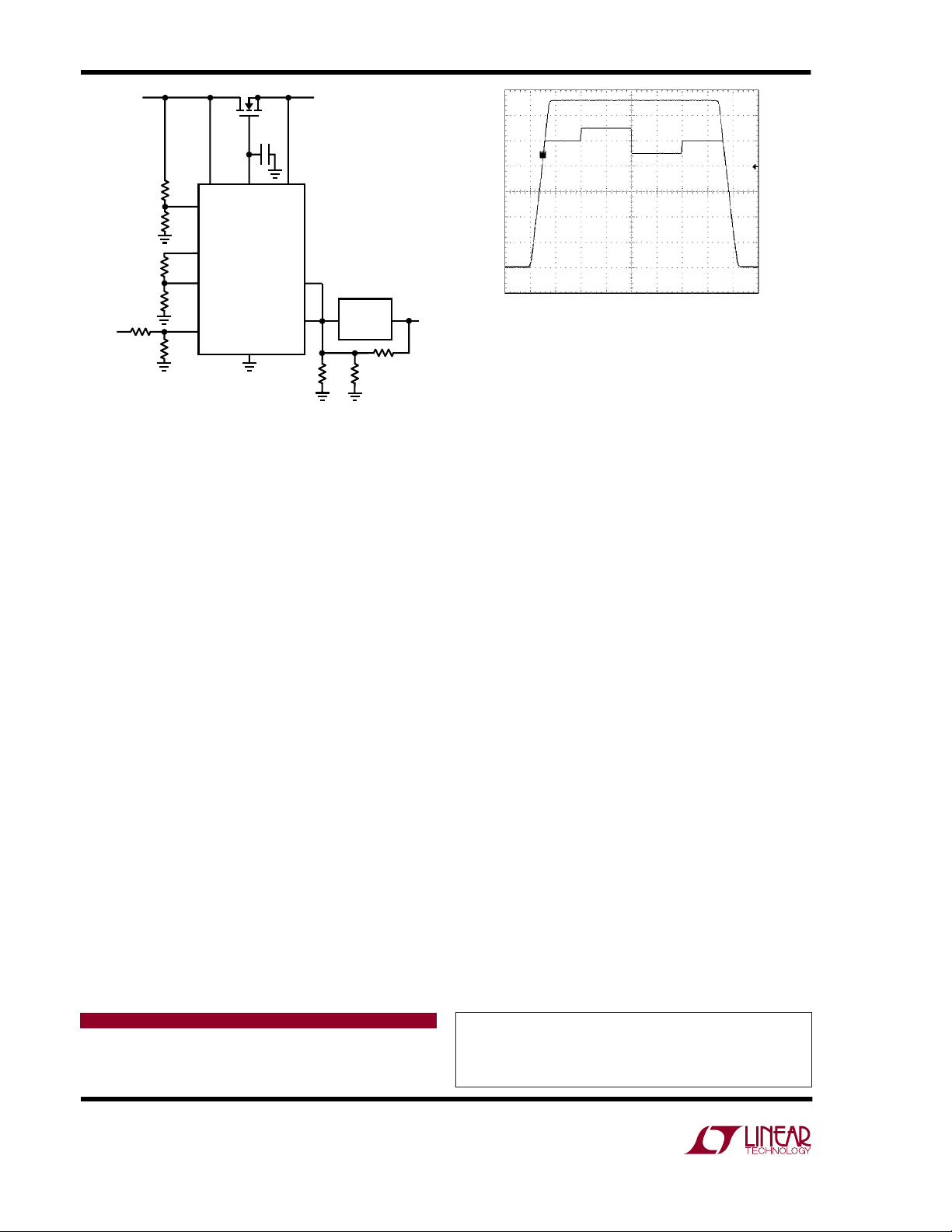
In the circuit shown in Figure 3, an LTC2923 ramps up a
3.3V supply through a series FET, tracks a 2.5V supply to
that 3.3V supply, and margins the 2.5V supply up and
down by 10%. The first tracking cell connected to pins
TRACK1 and FB1 causes the 2.5V supply to track this 3.3V
supply during power up and power down as shown in
Figure 4. The tracking cell connected to TRACK2 and FB2
is used to margin the 2.5V supply up and down by 10%.
The operation of the circuit in Figure 3 is simple. To margin
high, the I/O pin is pulled above 1.6V. This pulls the
TRACK2 pin above 0.8V so that no current is sourced into
the feedback node of the power supply. The supply then
defaults to its margined high output of 2.75V. For a
nominal output, the I/O is high impedance. Now, no
, LTC and LT are registered trademarks of Linear Technology Corporation.
All other trademarks are the property of their respective owners.
09/05/372
Page 2
V
CC
ON
RAMPBUF
TRACK1
TRACK2
Q1
C
0.1µF
GATE
LTC2923
GND
GATE
RAMP
FB1
FB2
R
FM1
54.4k
3.3V
DC/DC
FB
OUT
0.8V
R
F1
8k
DN372 F03
R
17k
2.5V
F2
3-STATE
I/O
V
3.3V
IN
R
TM2
54.4k
R
ON2
138k
R
ON1
100k
R
T2
17k
R
T1
8k
R
TM1
54.4k
Figure 3. The 2.5V Supply Tracks the 3.3V Supply and
Can be Margined High or Low by 10% Under Control of
a Three-State I/O
current flows through R
R
and is mirrored at the feedback node of the power
TM1
but 14.7µA flows through
TM2
supply. This forces the output voltage down by 250mV to
2.50V. For a margined low output, the I/O pin is pulled to
ground. Now, 14.7µA flows through R
the 14.7µA flowing through R
. This current is mirrored
TM1
in addition to
TM2
at the power supply feedback node, and drives the output
down by an extra 250mV from nominal.
Note that the ability to configure a current driven into the
feedback node with R
often allows the nominal output
TM1
voltage to be closer to the ideal value than is possible with
a single pair of standard value resistors, R
and RF2, in
F1
the power supply feedback network.
3.3V
2.5V
0.5V/DIV
10%
50ms/DIV
10%
DN372 F04
Figure 4. Output of Circuit in Figure 3. The 2.5V Supply
Tracks the 3.3V Supply and is Margined High and Low by
10%
If the desired high and low voltage margins, ∆V
, are not equal simply adjust R
∆V
LOW
choose R
set R
TM1
the voltage step ∆V
= ∆V
LOW
as above to configure the high margin, and
FM1
= R
. Scale the voltage step ∆V
FM1
by choosing R
HIGH
/∆V
. For example, to change the margins in
HIGH
. In this case,
TM2
LOW
by R
TM2
the above example to 10% high and 20% low, leave R
and R
unchanged at 54.4k, but reduce R
TM1
and
HIGH
relative to
TM1/RTM2
FM1
is to
TM2
27.2k.
If the feedback voltage, V
0.8V then the values of R
0.8V/V
were 1.23V, then R
R
. If the feedback voltage in the above example
FB
TM1
TM1
= R
TM2
= R
FM1
, of the power supply is not
FB
TM1
and R
and R
would be scaled so that
TM2
are scaled by
TM2
• 0.8V/1.23V = 35.4k.
Conclusion
The LTC2923’s primary application is tracking power
supplies, but its versatile architecture is suited to other
functions as well. The application described here allows a
three-state I/O to control supply margining using a few
resistors and an LTC2923 tracking cell.
Data Sheet Download
http://www.linear.com
Linear Technology Corporation
1630 McCarthy Blvd., Milpitas, CA 95035-7417
(408) 432-1900 ● FAX: (408) 434-0507 ● www.linear.com
For applications help,
call (408) 432-1900, Ext. 2452
dn372f LT/TP 0905 409K • PRINTED IN THE USA
© LINEAR TECHNOLOGY CORPORATION 2005
 Loading...