

Driving a Low Noise, Low Distortion 18-Bit, 1.6Msps ADC
C5
AMPLITUDE (dBFS)
0
Design Note 494
Guy Hoover
Introduction
The LTC®237 9 -18 is an 18-bit, 1.6Msps SAR ADC with
an extremely high SNR of 101dB and THD of –120dB. It
also features a unique digital-gain compression function,
which eliminates the need for a negative supply in the
ADC driver circuit.
Designing a driver circuit to get the best possible performance from the LTC2379-18 is not difficult. The two
circuits presented here demonstrate differential and
single-ended solutions using dual and single supplies.
Note that the components used here have been carefully
chosen with the ADC’s accuracy and acquisition time
requirements in mind, so any modifications should be
thoroughly tested.
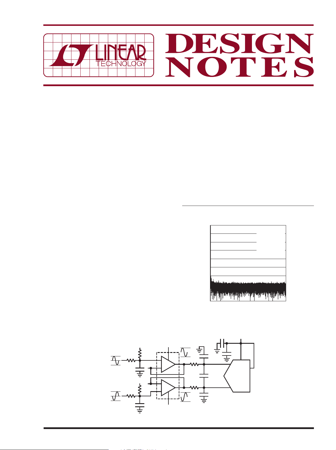
Fully Differential Driver
The circuit of Figure 1 converts a fully differential ±5V
signal to a fully differential 0V to 5V signal—the normal
input range for the LTC2379-18. This circuit is useful for
sensors that produce a fully differential output.
Filter networks R3, R5, C6 and R4, R6, C7 limit the input
bandwidth to approximately 100kHz. Matching on these
networks is important to achieve the lowest distortion,
as a mismatch in delay results in the development of a
common mode signal. The filter network comprising R1,
R2, C1, C2 and C3 minimizes the noise contribution of
the LT®6203 and minimizes disturbances reflected into
the LT6203 from sampling transients. The 32k point FFT
in Figure 2 shows the performance of the LTC2379-18 in
the circuit of Figure 1.
Single Supply Driver
The circuit of Figure 3 uses the digital gain compression
feature of the LTC2379-18, which de fines the ADC full-scal e
input swing to be 10% to 90% of the reference voltage.
This means that for a 5V reference the full-scale swing is
L, LT, LTC, LTM, Linear Technology and the Linear logo are registered trademarks of
Linear Technology Corporation. All other trademarks are the property of their respective
owners.
SNR = 101.2dB
–20
–40
–60
–80
–100
–120
–140
–160
–180
0 100 200 300 400 800700600500
FREQUENCY (kHz)
Figure 2. 32k Point FFT Using the Circuit of Figure 1
THD = –120dB
SINAD = 101.1dB
SFDR = 121dB
f
= 1.6Msps
S
= 2kHz
f
IN
DN494 F02
09/11/494
–5V
–5V
0.1µF
+
= 8V
5V
R3
1k
NPO
R4
1k
NPO
R5
1k
C6
5V
R6
1k
C7
V
IN
5V
0V
3300pF
V
IN
5V
0V
3300pF
V
8
+
V
3
+
2
–
LT6203
–
6
+
5
–
V
= –3.6V
–
V
4
5V
0V
1
R1
15Ω
R2
15Ω
7
5V
0V
C3
3300pF
NPO
C1
3300pF
NPO
C2
3300pF
NPO
5V
C4
47µF
REF
+
REF/DGC
LTC2379-18
–
DN494 F01
Figure 1. An LTC2379-18 Fully Differential ±5V Driver Using the LT®6203
+
= 5.5V
V
R18
1k
C42
10µF
±10V
–10V
R37
1k
V
IN
10V
R9
6.04k
+IN1
8
R15
4.32k
–IN1
1
R35
C45
10µF
15k
+IN2
2
0V
3
+
V
+
–
LT6350
415Ω
–
+
SHDN
–
V
6
7
OUT1
OUT2
4.5V
0.5V
4
5
4.5V
0.5V
Figure 3. LTC2379-18 Single Supply, ±10V Single-Ended Driver Using the LT6350
0.5V to 4.5V. This is sufficient headroom for the LT6350,
so a negative supply is not needed. This not only saves
the cost and complexity of providing a negative supply, it
also reduces the overall power consumption of the ADC
driver portion of the circuit by a factor of two.
R45
3.01k
R32
20Ω
R36
20Ω
C20
47µF
C19
3300pF
NPO
C40
3300pF
NPO
C39
3300pF
NPO
LTC2379-18
C56
0.1µF
+
–
REF
GND
C11
0.1µF
5V
REF/DGC
CHAIN
BUSY
OV
CNV
SCK
SDO
RD
V
DD
DD
V
IN
LTC6655-5
VO_F
VO_S
GND
2.5V
C10
0.1µF
3.3V
C7
0.1µF
R7
1k
C9
10µF
C6
10µF
DN494 F03
By using the LTC6655-5 precision low noise reference,
which only requires a supply 0.5V above its output, the
entire circuit can be operated from a single 5.5V supply.
This circuit ac cepts a ±10V single-ended input voltage and
converts it to a 0.5V to 4.5V fully differential signal. SNR
for this circuit is 99dB due to the reduced input swing
and THD is still a very good –95dB.
Layout Considerations
When dealing with a high speed 18-bit ADC, PC board
layout must be carefully considered. Always use a ground
plane. Keep traces as short as possible. Keep bypass
capacitors as close to the supply pins as possible. Each
bypass capacitor should have its own low impedance
return to ground. The analog input traces should be
screened by ground. The layout involving the ADC analog inputs should be as symmetrical as possible so that
parasitic elements cancel each other out. The output of
the reference and the REF pin bypass capacitors should
be as close to the REF pin as possible.
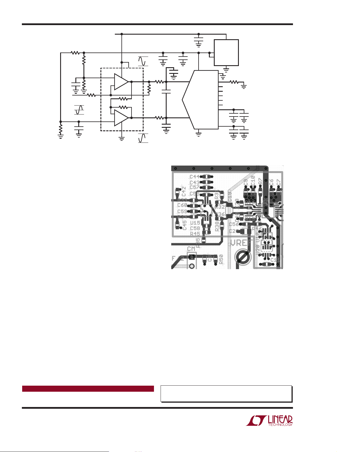
Figure 4 shows a sample layout for the LTC2379 -18.
Figure 4 is a composite of the top, ground, bottom and
silk screen layers. Component numbers used in the circui t
Figure 4. LTC2379-18 Sample Layout
of Figure 3 refer to layout of Figure 4. See the DC1783A
demo board manual available at www.linear.com for a
complete LTC2379-18 layout example.
Conclusion
Driving the LTC2379-18 is not difficult. Using the simple
circuits described here, the LTC2379-18 can be driven
over a variety of input voltage ranges with fully differential or single-ended inputs. With its unique digital-gain
compression function, the LTC2379-18 can be driven
with a single supply, which saves power while reducing
cost and complexity.
Data Sheet Download
www.linear.com/2379
Linear Technology Corporation
1630 McCarthy Blvd., Milpitas, CA 95035-7417
(408) 432-1900 ● FAX: (408) 434-0507 ● www.linear.com
For applications help,
call (408) 432-1900
dn494f LT/AP 0911 226K • PRINTED IN THE USA
LINEAR TECHNOLOGY CORPORATION 2011
 Loading...