

FEATURES
www.BDTIC.com/LINEAR
■
Sample Rate: 80Msps
■
Single 3V Supply (2.7V to 3.4V)
■
Low Power: 222mW
■
73dB SNR at 70MHz Input
■
90dB SFDR at 70MHz Input
■
No Missing Codes
■
Flexible Input: 1V
■
575MHz Full Power Bandwidth S/H
■
Clock Duty Cycle Stabilizer
■
Shutdown and Nap Modes
■
Pin Compatible Family
P-P
to 2V
P-P
Range
125Msps: LTC2253 (12-Bit), LTC2255 (14-Bit)
105Msps: LTC2252 (12-Bit), LTC2254 (14-Bit)
80Msps: LTC2229 (12-Bit), LTC2249 (14-Bit)
65Msps: LTC2228 (12-Bit), LTC2248 (14-Bit)
40Msps: LTC2227 (12-Bit), LTC2247 (14-Bit)
25Msps: LTC2226 (12-Bit), LTC2246 (14-Bit)
10Msps: LTC2225 (12-Bit), LTC2245 (14-Bit)
■
32-Pin (5mm × 5mm) QFN Package
U
APPLICATIO S
LTC2249
14-Bit, 80Msps
Low Power 3V ADC
U
DESCRIPTIO
The LTC®2249 is a 14-bit 80Msps, low power 3V A/D
converter designed for digitizing high frequency, wide
dynamic range signals. The LTC2249 is perfect for demanding imaging and communications applications with
AC performance that includes 73dB SNR and 90dB SFDR
for signals well beyond the Nyquist frequency.
DC specs include ±1LSB INL (typ), ±0.5LSB DNL (typ) and
no missing codes over temperature. The transition noise
is a low 1.2LSB
A single 3V supply allows low power operation. A separate
output supply allows the outputs to drive 0.5V to 3.6V
logic.
A single-ended CLK input controls converter operation. An
optional clock duty cycle stabilizer allows high performance at full speed for a wide range of clock duty cycles.
, LTC and LT are registered trademarks of Linear Technology Corporation.
All other trademarks are the property of their respective owners.
RMS
.
■
Wireless and Wired Broadband Communication
■
Imaging Systems
■
Ultrasound
■
Spectral Analysis
■
Portable Instrumentation
U
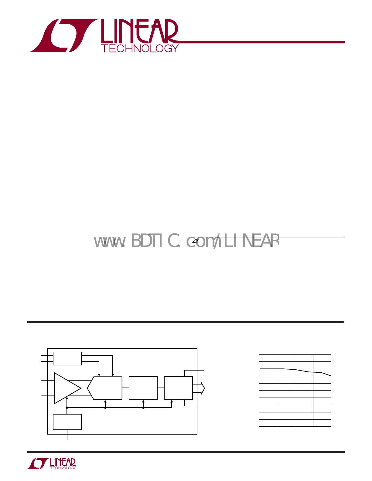
TYPICAL APPLICATIO
REFH
REFL
ANALOG
INPUT
FLEXIBLE
REFERENCE
+
INPUT
S/H
–
CLOCK/DUTY
CYCLE
CONTROL
CLK
14-BIT
PIPELINED
ADC CORE
CORRECTION
LOGIC
OUTPUT
DRIVERS
2229 TA01
OV
DD
D13
•
•
•
D0
OGND
SNR vs Input Frequency,
–1dB, 2V Range
75
74
73
72
71
70
69
SNR (dBFS)
68
67
66
65
50
0
INPUT FREQUENCY (MHz)
100
150
200
2249 G09
2249fa
1
LTC2249
www.BDTIC.com/LINEAR
WW
W
U
ABSOLUTE AXI U RATI GS
OVDD = VDD (Notes 1, 2)
Supply Voltage (VDD) ................................................. 4V
Digital Output Ground Voltage (OGND) ....... –0.3V to 1V
Analog Input Voltage (Note 3) ..... –0.3V to (V
Digital Input Voltage .................... –0.3V to (V
Digital Output Voltage ................– 0.3V to (OV
Power Dissipation............................................ 1500mW
Operating Temperature Range
LTC2249C ............................................... 0°C to 70°C
LTC2249I............................................. –40°C to 85°C
Storage Temperature Range ..................–65°C to 125°C
+ 0.3V)
DD
+ 0.3V)
DD
+ 0.3V)
DD
UUW
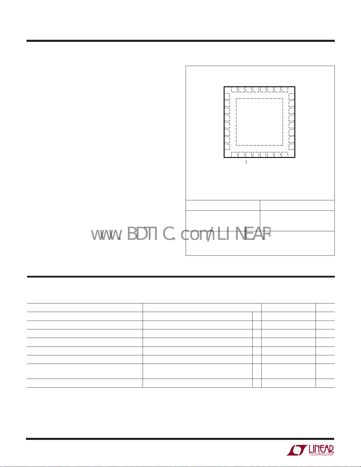
PACKAGE/ORDER I FOR ATIO
TOP VIEW
VDDVCMSENSE
32 31 30 29 28 27 26 25
+
1AIN
–
AIN
2
REFH
3
REFH
4
REFL
5
REFL
6
V
7
DD
GND
8
9 10 11 12
CLK
32-LEAD (5mm × 5mm) PLASTIC QFN
T
JMAX
EXPOSED PAD IS GND (PIN 33)
MUST BE SOLDERED TO PCB
ORDER PART NUMBER
LTC2249CUH
LTC2249IUH
MODEOFD13
33
13 14 15 16
OED0D1D2D3
SHDN
UH PACKAGE
= 125°C, θJA = 34°C/W
QFN PART MARKING*
D12
D11
24
23
22
21
20
19
18
17
D4
2249
D10
D9
D8
OV
DD
OGND
D7
D6
D5
Order Options Tape and Reel: Add #TR
Lead Free: Add #PBF Lead Free Tape and Reel: Add #TRPBF
Lead Free Part Marking: http://www.linear.com/leadfree/
Consult LTC Marketing for parts specified with wider operating temperature ranges.
*The temperature grade is identified by a label on the shipping container.
U
CO VERTER CHARACTERISTICS
temperature range, otherwise specifications are at TA = 25°C. (Note 4)
PARAMETER CONDITIONS MIN TYP MAX UNITS
Resolution (No Missing Codes) ● 14 Bits
Integral Linearity Error Differential Analog Input (Note 5) ● –4 ±1 4 LSB
Differential Linearity Error Differential Analog Input ● –1 ±0.5 1 LSB
Offset Error (Note 6) ● –12 ±212 mV
Gain Error External Reference ● –2.5 ±0.5 2.5 %FS
Offset Drift ±10 µV/°C
Full-Scale Drift Internal Reference ±30 ppm/°C
Transition Noise SENSE = 1V 1.2 LSB
The ● denotes the specifications which apply over the full operating
External Reference ±5 ppm/°C
RMS
2
2249fa
LTC2249
www.BDTIC.com/LINEAR
UU
A ALOG I PUT
specifications are at T
SYMBOL PARAMETER CONDITIONS MIN TYP MAX UNITS
V
IN
V
IN,CM
I
IN
I
SENSE
I
MODE
t
AP
t
JITTER
CMRR Analog Input Common Mode Rejection Ratio 80 dB
U
W
A
Analog Input Range (A
Analog Input Common Mode (A
Analog Input Leakage Current 0V < A
SENSE Input Leakage 0V < SENSE < 1V ● –3 3 µA
MODE Pin Leakage ● –3 3 µA
Sample-and-Hold Acquisition Delay Time 0 ns
Sample-and-Hold Acquisition Delay Time Jitter 0.2 ps
DY A IC ACCURACY
otherwise specifications are at TA = 25°C. AIN = –1dBFS. (Note 4)
SYMBOL PARAMETER CONDITIONS MIN TYP MAX UNITS
SNR Signal-to-Noise Ratio 5MHz Input 73 dB
SFDR Spurious Free Dynamic Range 5MHz Input 90 dB
2nd or 3rd Harmonic
SFDR Spurious Free Dynamic Range 5MHz Input 95 dB
4th Harmonic or Higher
S/(N+D) Signal-to-Noise Plus Distortion Ratio 5MHz Input 72.9 dB
I
MD
Intermodulation Distortion f
Full Power Bandwidth Figure 8 Test Circuit 575 MHz
The ● denotes the specifications which apply over the full operating temperature range, otherwise
= 25°C. (Note 4)
+
–
– A
IN
) 2.7V < V
IN
+
–
+ A
IN
)/2 Differential Input (Note 7) ● 1 1.5 1.9 V
IN
Single Ended Input (Note 7)
< 3.4V (Note 7) ● ±0.5 to ±1V
DD
● 0.5 1.5 2 V
+
–
, A
< V
IN
IN
DD
● –1 1 µA
The ● denotes the specifications which apply over the full operating temperature range,
40MHz Input ● 70.8 73 dB
70MHz Input 73 dB
140MHz Input 72.6 dB
40MHz Input
70MHz Input 90 dB
140MHz Input 85 dB
40MHz Input
70MHz Input 95 dB
140MHz Input 90 dB
40MHz Input ● 70.2 72.8 dB
70MHz Input 72.8 dB
140MHz Input 72.1 dB
= 28.2MHz, f
IN1
= 26.8MHz 90 dB
IN2
● 75 90 dB
● 81 95 dB
RMS
UU U
I TER AL REFERE CE CHARACTERISTICS
(Note 4)
PARAMETER CONDITIONS MIN TYP MAX UNITS
VCM Output Voltage I
VCM Output Tempco ±25 ppm/°C
VCM Line Regulation 2.7V < VDD < 3.4V 3 mV/V
VCM Output Resistance –1mA < I
OUT
= 0 1.475 1.500 1.525 V
< 1mA 4 Ω
OUT
2249fa
3
LTC2249
www.BDTIC.com/LINEAR
UU
DIGITAL I PUTS A D DIGITAL OUTPUTS
full operating temperature range, otherwise specifications are at T
SYMBOL PARAMETER CONDITIONS MIN TYP MAX UNITS
LOGIC INPUTS (CLK, OE, SHDN)
V
IH
V
IL
I
IN
C
IN
LOGIC OUTPUTS
OVDD = 3V
C
OZ
I
SOURCE
I
SINK
V
OH
V
OL
OV
= 2.5V
DD
V
OH
V
OL
OVDD = 1.8V
V
OH
V
OL
High Level Input Voltage VDD = 3V ● 2V
Low Level Input Voltage VDD = 3V ● 0.8 V
Input Current VIN = 0V to V
Input Capacitance (Note 7) 3 pF
Hi-Z Output Capacitance OE = High (Note 7) 3 pF
Output Source Current V
Output Sink Current V
High Level Output Voltage IO = –10µA 2.995 V
Low Level Output Voltage IO = 10µA 0.005 V
High Level Output Voltage IO = –200µA 2.49 V
Low Level Output Voltage IO = 1.6mA 0.09 V
High Level Output Voltage IO = –200µA 1.79 V
Low Level Output Voltage IO = 1.6mA 0.09 V
= 25°C. (Note 4)
A
= 0V 50 mA
OUT
= 3V 50 mA
OUT
= –200µA ● 2.7 2.99 V
I
O
= 1.6mA ● 0.09 0.4 V
I
O
The ● denotes the specifications which apply over the
DD
● –10 10 µA
WU
POWER REQUIRE E TS
range, otherwise specifications are at TA = 25°C. (Note 8)
SYMBOL PARAMETER CONDITIONS MIN TYP MAX UNITS
V
OV
IV
P
P
P
DD
DD
DD
DISS
SHDN
NAP
Analog Supply Voltage (Note 9) ● 2.7 3 3.4 V
Output Supply Voltage (Note 9) ● 0.5 3 3.6 V
Supply Current ● 74 86 mA
Power Dissipation ● 222 258 mW
Shutdown Power SHDN = H, OE = H, No CLK 2 mW
Nap Mode Power SHDN = H, OE = L, No CLK 15 mW
The ● denotes the specifications which apply over the full operating temperature
4
2249fa
LTC2249
www.BDTIC.com/LINEAR
UW
TI I G CHARACTERISTICS
range, otherwise specifications are at TA = 25°C. (Note 4)
SYMBOL PARAMETER CONDITIONS MIN TYP MAX UNITS
f
s
t
L
t
H
t
AP
t
D
Pipeline 5 Cycles
Latency
Sampling Frequency (Note 9) ● 1 80 MHz
CLK Low Time Duty Cycle Stabilizer Off ● 5.9 6.25 500 ns
CLK High Time Duty Cycle Stabilizer Off ● 5.9 6.25 500 ns
Sample-and-Hold Aperture Delay 0ns
CLK to DATA Delay CL = 5pF (Note 7) ● 1.4 2.7 5.4 ns
Data Access Time After OE↓ CL = 5pF (Note 7) ● 4.3 10 ns
BUS Relinquish Time (Note 7) ● 3.3 8.5 ns
The ● denotes the specifications which apply over the full operating temperature
Duty Cycle Stabilizer On (Note 7)
Duty Cycle Stabilizer On (Note 7)
● 5 6.25 500 ns
● 5 6.25 500 ns
Note 1: Stresses beyond those listed under Absolute Maximum Ratings
may cause permanent damage to the device. Exposure to any Absolute
Maximum Rating condition for extended periods may affect device
reliability and lifetime.
Note 2: All voltage values are with respect to ground with GND and OGND
wired together (unless otherwise noted).
Note 3: When these pin voltages are taken below GND or above V
DD
, they
will be clamped by internal diodes. This product can handle input currents
of greater than 100mA below GND or above V
Note 4: VDD = 3V, f
= 80MHz, input range = 2V
SAMPLE
without latchup.
DD
with differential
P-P
Note 5: Integral nonlinearity is defined as the deviation of a code from a
straight line passing through the actual endpoints of the transfer curve.
The deviation is measured from the center of the quantization band.
Note 6: Offset error is the offset voltage measured from –0.5 LSB when
the output code flickers between 00 0000 0000 0000 and
11 1111 1111 1111.
Note 7: Guaranteed by design, not subject to test.
Note 8: VDD = 3V, f
differential drive.
Note 9: Recommended operating conditions.
drive, unless otherwise noted.
UW
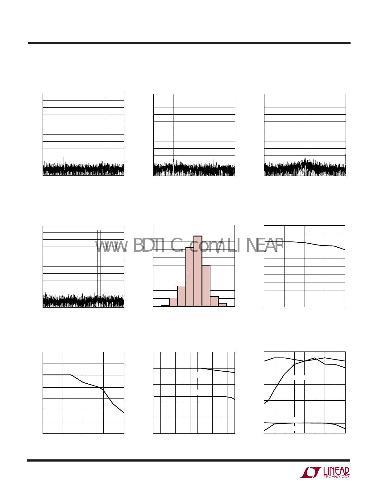
TYPICAL PERFOR A CE CHARACTERISTICS
Typical INL, 2V Range
2.0
1.5
1.0
0.5
0
–0.5
INL ERROR (LSB)
–1.0
–1.5
–2.0
0
4096
8192
CODE
12288
16384
2249 G01
Typical DNL, 2V Range
1.0
0.8
0.6
0.4
0.2
0
–0.2
DNL ERROR (LSB)
–0.4
–0.6
–0.8
–1.0
0
4096
8192
CODE
12288
16384
2249 G02
= 80MHz, input range = 1V
SAMPLE
8192 Point FFT, fIN = 5MHz,
–1dB, 2V Range
0
–10
–20
–30
–40
–50
–60
–70
AMPLITUDE (dB)
–80
–90
–100
–110
–120
5
0
with
P-P
15
FREQUENCY (MHz)
2510
20
30
35
40
2249 G03
2249fa
5
LTC2249
CLOCK DUTY CYCLE (%)
30
SNR AND SFDR (dBFS)
85
90
60
2249 G12
80
75
40 50
35 65
45 55 70
70
95
SFDR: DCS ON
SNR: DCS ON
SNR: DCS OFF
SFDR: DCS OFF
www.BDTIC.com/LINEAR
UW
TYPICAL PERFOR A CE CHARACTERISTICS
8192 Point FFT, fIN = 30MHz,
–1dB, 2V Range
0
–10
–20
–30
–40
–50
–60
–70
AMPLITUDE (dB)
–80
–90
–100
–110
–120
5
0
15
20
FREQUENCY (MHz)
8192 Point 2-Tone FFT,
fIN = 28.2MHz and 26.8MHz,
–1dB, 2V Range
0
–10
–20
–30
–40
–50
–60
–70
AMPLITUDE (dB)
–80
–90
–100
–110
–120
5
0
15
20
FREQUENCY (MHz)
8192 Point FFT, fIN = 70MHz,
–1dB, 2V Range
0
–10
–20
–30
–40
–50
–60
–70
AMPLITUDE (dB)
–80
–90
–100
–110
2510
30
35
40
2249 G04
–120
5
0
15
FREQUENCY (MHz)
2510
30
35
20
40
2249 G05
8192 Point FFT, fIN = 140MHz,
–1dB, 2V Range
0
–10
–20
–30
–40
–50
–60
–70
AMPLITUDE (dB)
–80
–90
–100
–110
–120
5
0
15
20
FREQUENCY (MHz)
2510
30
35
40
2249 G06
SNR vs Input Frequency,
Grounded Input Histogram
50000
35969
43161
CODE
25292
6150
1987
178
2249 G08
45000
40000
35000
30000
25000
COUNT
20000
15000
10000
5000
26
0
2510
30
35
40
2249 G07
8201
12558
5194
552
8203 8205 8207 8209
–1dB, 2V Range
75
74
73
72
71
70
69
SNR (dBFS)
68
67
66
65
0
50
INPUT FREQUENCY (MHz)
100
150
200
2249 G09
SFDR vs Input Frequency,
–1dB, 2V Range
100
95
90
85
80
SFDR (dBFS)
75
70
65
6
50 100 200
0
INPUT FREQUENCY (MHz)
150
2249 G10
SNR and SFDR vs Sample Rate,
2V Range, fIN = 5MHz, –1dB
100
90
80
70
SNR AND SFDR (dBFS)
60
50
10 20 30
0
40 50
SAMPLE RATE (Msps)
SFDR
SNR
60 70 90 100
80
SNR and SFDR
vs Clock Duty Cycle
110
2249 G11
2249fa
UW
www.BDTIC.com/LINEAR
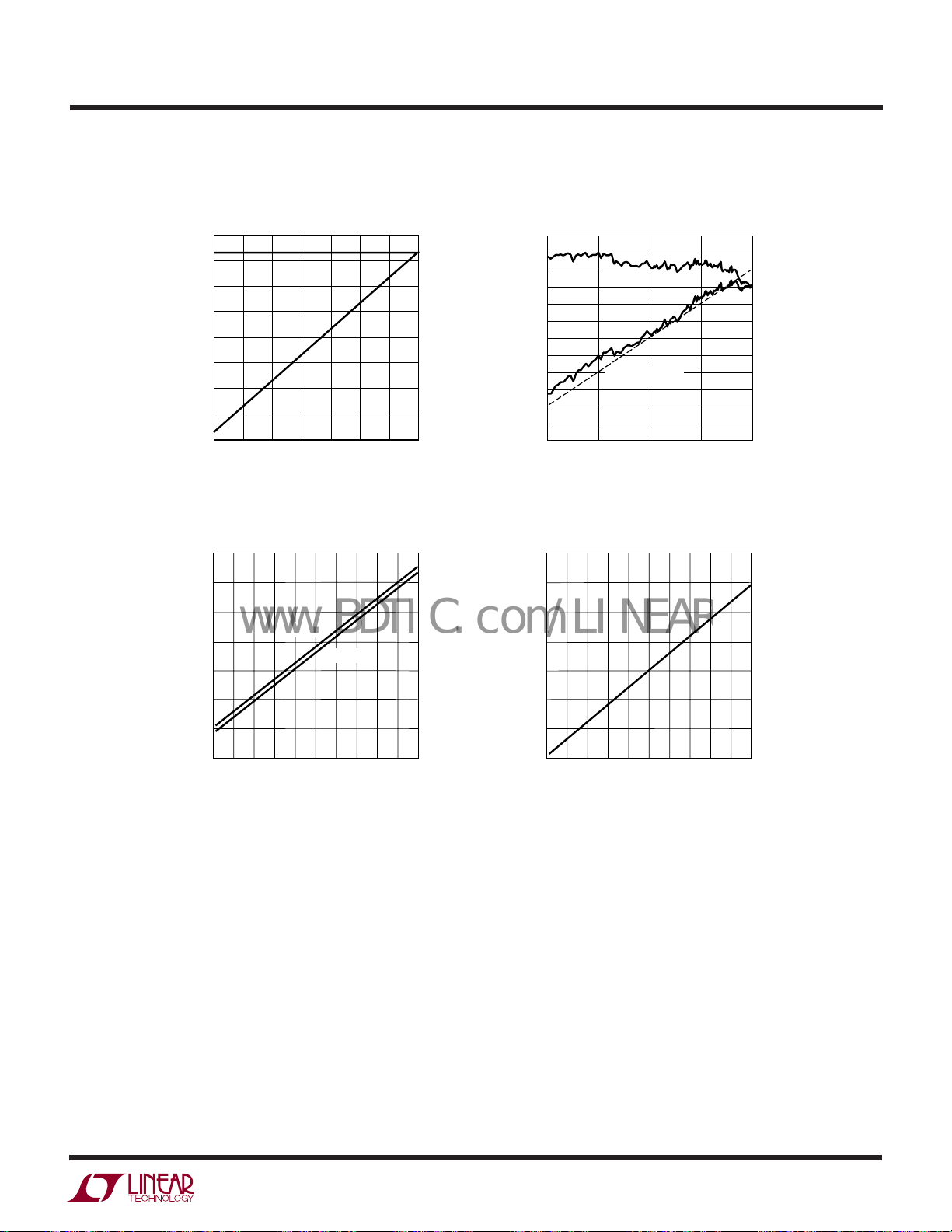
TYPICAL PERFOR A CE CHARACTERISTICS
LTC2249
SNR vs Input Level,
fIN = 70MHz, 2V Range
80
70
60
50
40
30
SNR (dBc AND dBFS)
20
10
0
I
VDD
dBFS
dBc
–40 –30
–50–60–70
INPUT LEVEL (dBFS)
vs Sample Rate,
5MHz Sine Wave Input, –1dB
85
80
75
(mA)
VDD
I
70
65
2V RANGE
1V RANGE
–20
–10
2249 G13
SFDR vs Input Level,
fIN = 70MHz, 2V Range
120
110
100
90
80
70
60
50
40
SFDR (dBc AND dBFS)
30
20
10
0
0
–80
I
OVDD
Wave Input, –1dB, O
7
6
5
(mA)
4
OVDD
I
3
dBFS
dBc
100dBc SFDR
REFERENCE LINE
–60
–40
INPUT LEVEL (dBFS)
–20
2249 G14
vs Sample Rate, 5MHz Sine
= 1.8V
VDD
0
60
55
50
0
30
20
10
SAMPLE RATE (Msps)
40
60 80
50
70
90
2249 G15
100
2
1
0
0
30
20
10
SAMPLE RATE (Msps)
40
50
70
60 80
90
2249 G16
100
2249fa
7
LTC2249
www.BDTIC.com/LINEAR
U
UU
PI FU CTIO S
AIN+ (Pin 1): Positive Differential Analog Input.
- (Pin 2): Negative Differential Analog Input.
A
IN
REFH (Pins 3, 4): ADC High Reference. Short together and
bypass to pins 5, 6 with a 0.1µF ceramic chip capacitor as
close to the pin as possible. Also bypass to pins 5, 6 with
an additional 2.2µF ceramic chip capacitor and to ground
with a 1µF ceramic chip capacitor.
REFL (Pins 5, 6): ADC Low Reference. Short together and
bypass to pins 3, 4 with a 0.1µF ceramic chip capacitor as
close to the pin as possible. Also bypass to pins 3, 4 with
an additional 2.2µF ceramic chip capacitor and to ground
with a 1µF ceramic chip capacitor.
V
(Pins 7, 32): 3V Supply. Bypass to GND with 0.1µF
DD
ceramic chip capacitors.
GND (Pin 8): ADC Power Ground.
CLK (Pin 9): Clock Input. The input sample starts on the
positive edge.
SHDN (Pin 10): Shutdown Mode Selection Pin. Connecting SHDN to GND and OE to GND results in normal
operation with the outputs enabled. Connecting SHDN to
GND and OE to VDD results in normal operation with the
outputs at high impedance. Connecting SHDN to VDD and
OE to GND results in nap mode with the outputs at high
impedance. Connecting SHDN to VDD and OE to V
results in sleep mode with the outputs at high impedance.
OE (Pin 11): Output Enable Pin. Refer to SHDN pin
function.
DD
D0 – D13 (Pins 12, 13, 14, 15, 16, 17, 18, 19, 22, 23, 24,
25, 26, 27): Digital Outputs. D13 is the MSB.
OGND (Pin 20): Output Driver Ground.
OVDD (Pin 21): Positive Supply for the Output Drivers.
Bypass to ground with 0.1µF ceramic chip capacitor.
OF (Pin 28): Over/Under Flow Output. High when an over
or under flow has occurred.
MODE (Pin 29): Output Format and Clock Duty Cycle
Stabilizer Selection Pin. Connecting MODE to GND selects
offset binary output format and turns the clock duty cycle
stabilizer off. 1/3 VDD selects offset binary output format
and turns the clock duty cycle stabilizer on. 2/3 VDD selects
2’s complement output format and turns the clock duty
cycle stabilizer on. VDD selects 2’s complement output
format and turns the clock duty cycle stabilizer off.
SENSE (Pin 30): Reference Programming Pin. Connecting
SENSE to VCM selects the internal reference and a ±0.5V
input range. VDD selects the internal reference and a ±1V
input range. An external reference greater than 0.5V and
less than 1V applied to SENSE selects an input range of
±V
VCM (Pin 31): 1.5V Output and Input Common Mode Bias.
Bypass to ground with 2.2µF ceramic chip capacitor.
GND (Exposed Pad) (Pin 33): ADC Power Ground. The
exposed pad on the bottom of the package needs to be
soldered to ground.
. ±1V is the largest valid input range.
SENSE
8
2249fa
 Loading...