

Linear Technology LTC222CJ, LTC221CN, LTC221CJ, LTC222MJ, LTC222CS Datasheet
...
FEATURES
■
Micropower Operation
■
Single 5V or ±15V Supply Operation
■
Low Charge Injection
■
Low R
■
■
■
■
■
■
ON
Low Leakage
Guaranteed Break Before Make
Latch Resistant Design
TLL/CMOS Compatible
Improved Second Source for DG221/DG222
Microprocessor Bus Compatible
U
KEY SPECIFICATIO S
■
Supply Current ..................... I+ = 40µA, I– = 5µA Max
■
Charge Injection
±15V Supplies .................................±25pC Max
Single 5V Supply .................................. 2pC Typ
■
RON............................................................... 65ΩTyp
■
Signal Range ..................................................... ±15V
LTC221/LTC222
Micropower, Low Charge
Injection, Quad CMOS Analog
Switches with Data Latches
U
DESCRIPTIO
The LTC®221 and LTC222 are micropower, quad CMOS
analog switches which typically dissipate only 250µW
from ±15V supplies and 40µW from a single 5V supply.
Onboard latches allow the LTC221 and LTC222 to interface directly to most microprocessor buses. The switches
have 65Ω typical on resistance and a very high off resistance. A break before make characteristic is inherent in
these switches to prevent the shorting of two channels.
The signal range is ±15V with a supply voltage of ±15V and
0V to 5V with a single 5V supply. The switches have special
charge compensation circuitry which greatly reduces
charge injection to a maximum of ±25pC (±15V supplies).
The LTC221 and LTC222 are designed for applications
such as microprocessor controlled programmable gain
amplifiers, automatic test equipment, communication
systems, and data acquisition systems. The LTC221 is
normally closed and the LTC222 is normally open as
shown in the Logic Table.
, LTC and LT are registered trademarks of Linear Technology Corporation.
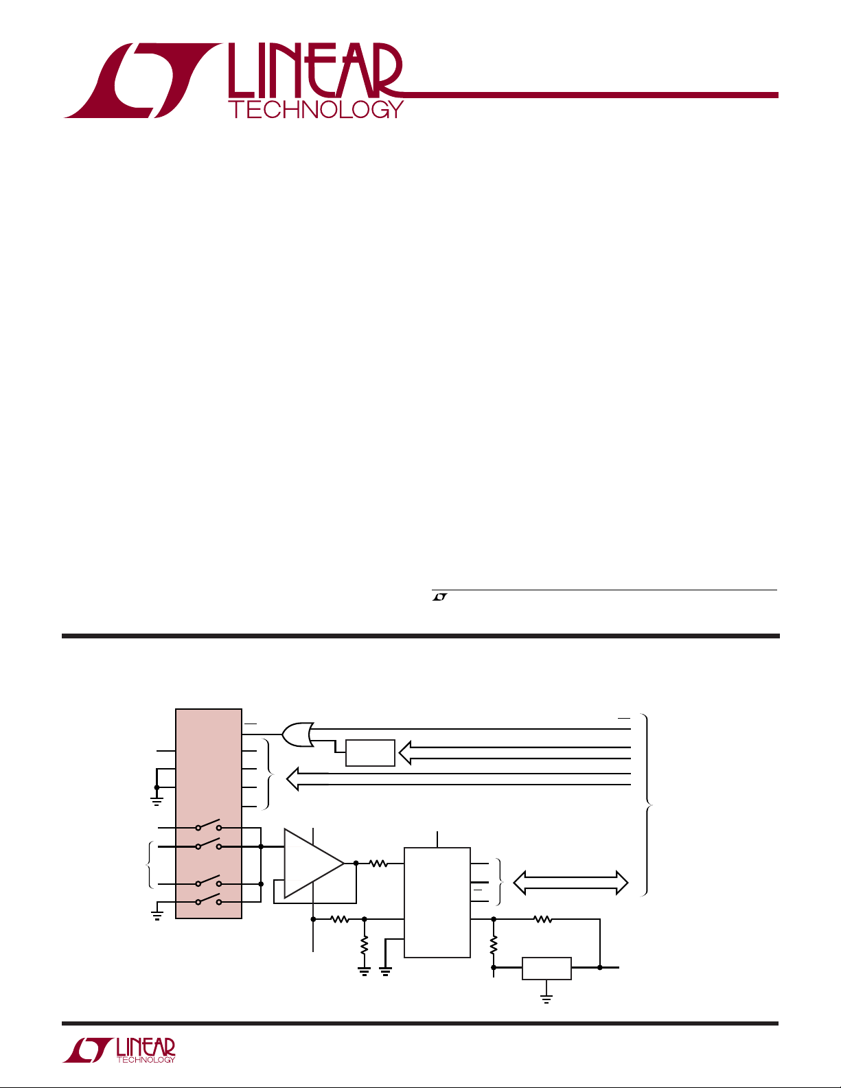
TYPICAL APPLICATIO
V
OV TO 5V
LTC221/LTC222
+
V
5V
GND IN3
–
V
V
FS
IN
WR
IN4
IN2
IN1
D1S1
D2S2
D3S3
D4S4
U
Two-Channel, 12-Bit, Self Calibrating Data Acquisition System
LOGIC
DECODER
DATA BUS B0 – B3
15V
+
LT1 006
–
–15V
10k
150k 100k
120Ω
–IN
GND
5V
LTC1292
IN
12-BIT
ADC
R1
ADDRESS BUS
CLK
D
OUT
CS
V
REF
270Ω
V
FS
SERIAL PORT
LT1027
WR
15V
LTC221/222 • TA01
TO MICROPROCESSOR
e.g. TMS320C25
2212fa
1
LTC221/LTC222
WWWU
ABSOLUTE AXI U RATI GS
(Note 1)
Voltages Referenced to V
+
V
...........................................................................................
GND..................................................................... 25V
Digital Inputs, S, D (Note 2) .......... –2V to (V+ 2V) or
Digital Inputs, S, D (N2020mA, Whichever Occurs First
Current
Any Input Except S or D ................................... 30mA
Continuous S or D ............................................ 20mA
Peak S or D
(Pulsed at 1 ms, 10% Duty Cycle Max) ......... 70mA
ESD Susceptibility (Note 3) ......................................4kV
Power Dissipation (Plastic) ............................... 500mW
Power Dissipation (Ceramic) ............................. 900mW
Operating Temperature Range
LTC221C/LTC222C .................................. 0°C to 70°C
LTC221M/LTC222M (OBSOLETE).......– 55°C to 125°C
Storage Temperature Range ................. –65°C to 150°C
Lead Temperature (Soldering, 10 sec).................. 300°C
–
44V
UU
W
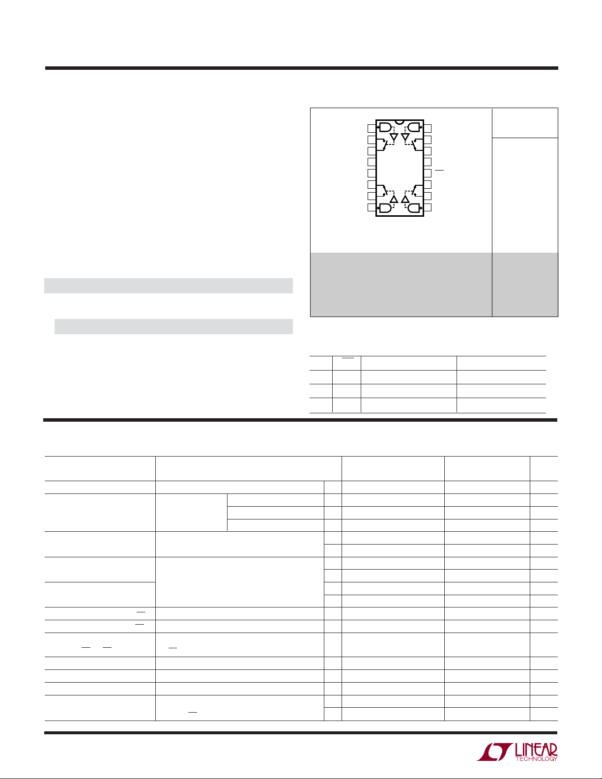
PACKAGE/ORDER I FOR ATIO
TOP VIEW
IN1
D1
S1
V
GND
S4
D4
IN4
N PACKAGE
16-LEAD PDIP
= 110°C, θJA = 120°C/W
J
MAX
1
2
3
–
4
5
6
7
8
J PACKAGE
16-LEAD CERDIP
16
IN2
15
D2
14
S2
+
13
V
12
WR
11
S3
10
D3
9
IN3
S PACKAGE
16-LEAD PLASTIC SO
= 110°C, θJA = 130°C/W
J
MAX
OBSOLETE PACKAGE
Consider the N or S Package for Alternate Source
Consult LTC Marketing for parts specified with wider operating temperature ranges.
ORDER PART
NUMBER
LTC221CN
LTC221CS
LTC222CN
LTC222CS
LTC221MJ
LTC221CJ
LTC222MJ
LTC222CJ
LOGIC TABLE
INX WR LTC221 LTC222
00 On Off
10 Off On
X1Maintain Previous State Maintain Previous State
U
DIGITAL A D DC ELECTRICAL CHARACTERISTICS
over full operating temperature range, otherwise specifications are at TA = 25°C. V+ = ±15V, V– = –15V, GND = 0V, unless noted.
PARAMETER CONDITIONS MIN TYP MAX MIN TYP MAX UNITS
Analog Signal Range
R
ON
Off Input Leakage IS (OFF) VD = 14V, VS = ±14V 0.01 ±1 0.01 ±5nA
Off Output Leakage ID (0FF) VIN = 2.4V, LTC221 0.01 ±1 0.01 ±5nA
On Channel Leakage lD (ON) VD = VS = ±14V, VIN = 2.4V, LTC222 0.02 ±1 0.02 ±5nA
Input High Voltage V
Input Low Voltage V
Input High or Low Current VIN = 15V, 0V
I
, I
, I
INH
INL
WRH, IWRL
CS (OFF) 55pF
CD (OFF) 12 12 pF
CD, CS (ON) 30 30 pF
+
I
INH
INL
, V
, V
VS = ±10V T
ID = 1mA 25°C65906590Ω
VIN = 0.8V, LTC222
VIN = 0.8V, LTC221
WRH
WRL
VWR = 15V, 0V
All Channels On or Off 16 40 16 40 µA
VIN = VWR = 0V or 4.0V
T
MIN
MAX
●
●
●
●
●
2.4 2.4 V
●
●
●
The ● denotes the specifications which apply
LTC221M/LTC222M LTC221C/LTC222C
±15 ±15 V
90 90 Ω
135 135 Ω
±100 ±100 nA
±100 ±100 nA
±200 ±200 nA
0.8 0.8 V
±1 ±1 µA
60 60 µA
2212fa
2
LTC221/LTC222
U
DIGITAL A D DC ELECTRICAL CHARACTERISTICS
over full operating temperature range, otherwise specifications are at T
PARAMETER CONDITIONS MIN TYP MAX MIN TYP MAX UNITS
–
I
= 25°C. V+ = ±15V, V– = –15V, GND = 0V, unless noted.
A
LTC221M/LTC222M LTC221C/LTC222C
0.1 5 0.1 5 µA
●
The ● denotes the specifications which apply
10 10
AC ELECTRICAL CHARACTERISTICS
V+ = 15V, V– = –15V, GND = 0V, unless otherwise noted.
LTC221M/LTC222M LTC221C/LTC222C
PARAMETER CONDITIONS MIN TYP MAX MIN TYP MAX UNITS
t
ON
t
OFF
t
OPEN
Off Isolation VS = 2Vp-p, RL = 1kΩ 75 75 dB
Crosstalk f = 100kHz 90 90
Charge Injection O
Total Harmonic Distortion THD VS = 2Vp-p, RL = 10kΩ 0.01 0.01 %
tON, WR VS = 2V, RL = 1kΩ, CL = 35pF 270 400 270 400 ns
t
, WR 160 300 160 300
OFF
INJ
VS = 2V, RL = 1kΩ, CL = 35pF 290 400 290 400 ns
210 300 210 300
20 85 20 85 ns
R
= 0Ω, CL = 1000pF, V
GEN
= 0 5 ±25 8 ±25 pC
GEN
U
DIGITAL A D DC ELECTRICAL CHARACTERISTICS
over full operating temperature range, otherwise specifications are at TA = 25°C. V+ = 5V, V– = GND = 0V, unless noted.
LTC221M/LTC222M LTC221C/LTC222C
PARAMETER CONDITIONS MIN TYP MAX MIN TYP MAX UNITS
Analog Signal Range
R
ON
Off Input Leakage IS (OFF) VD = 4V, 1V; VS = 1V, 4V 0.01 ±1 0.01 ± 5nA
Off Output Leakage ID (0FF) 0.01 ±1 0.01 ±5nA
On Channel Leakage lD (ON) VD = VS = 1V, 4V 0.01 ±1 0.01 ± 5nA
Input High Voltage V
Input Low Voltage V
Input High or Low Current VIN = 5V, 0V
I
, I
, I
INH
INL
WRH, IWRL
CS(OFF) 5 5 pF
CD (OFF) 12 12 pF
CD, CS (ON) 30 30 pF
+
I
INH
INL
, V
, V
WRL
VS = 1.5V, 3V T
ID = 0.25mA 25°C 280 450 280 520 Ω
(Note 4)
(Note 4)
WRH
VWR = 5V, 0V
All Channels On or Off 8 20 8 20 µA
VIN = VWR = 0V or 4.0V
T
MIN
MAX
●
0505 V
●
●
●
●
2.4 2.4 V
●
●
●
The ● denotes the specifications which apply
450 520 Ω
650 650 Ω
±100 ±100 nA
±100 ±100 nA
±200 ±200 nA
0.8 0.8 V
±1 ±1 µA
30 30 µA
2212fa
3
LTC221/LTC222
AC ELECTRICAL CHARACTERISTICS
V+ = 5V, V– = GND = 0V, unless otherwise noted.
LTC221M/LTC222M LTC221C/LTC222C
PARAMETER CONDITIONS MIN TYP MAX MIN TYP MAX UNITS
t
ON
t
OFF
t
OPEN
Off Isolation VS = 2V
VS = 2V, RL = 1kΩ, CL = 35pF 450 600 450 600 ns
190 300 190 300 ns
100 250 100 250 ns
, RL = 1kΩ 75 75 dB
P-P
Crosstalk f = 100kHz 90 90 dB
Charge Injection O
INJ
Total Harmonic Distortion THD VS = 2V
R
= 0Ω, CL = 1000pF, V
GEN
, RL = 10kΩ 0.01 0.01 %
P-P
= 2.5V 2 2 pC
GEN
tON, WR VS = 2V, RL = 1kΩ, CL = 35pF 430 600 430 600 ns
t
, WR 160 300 160 300 ns
OFF
Note 1: Absolute Maximum Ratings are those values beyond which the life
of a device may be impaired.
Note 2: Signals on S, D, or IN exceeding V
+
or V– will be clamped by
internal diodes. Limit forward diode current to maximum current rating.
Note 3: In-circuit ESD on the switch pins (S or D) exceeds 4kV (see test
circuit).
Note 4: Leakage current with a 5V supply is guaranteed by correlation with
the ±15V leakage current.
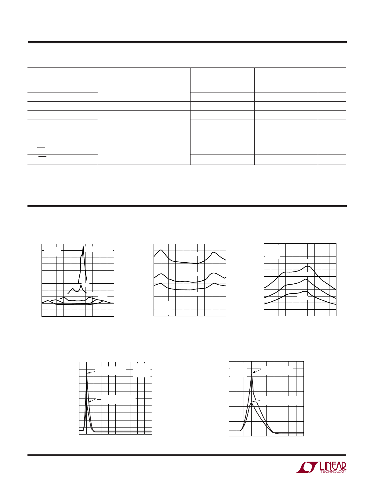
UW
TYPICAL PERFOR A CE CHARACTERISTICS
RON vs VS Over Supply Voltage
TA = 25°C
250
= 1mA
I
D
200
150
(Ω)
ON
R
100
50
0
–8
–16
–12–20 16
V
SUPPLY
±5V
±10V
–4
0
4
VS (V)
Positive Supply Current vs
Logic Input Voltage
250
200
150
(µA)
+
I
100
= 5V, OV
±15V
±20V
8
12
20
LTC221/222 • TPC01
ALL LOGIC INPUTS
TIED TOGETHER
ALL I
TIED TOGETHER
NX
WR TIED TO GROUND
(Ω)
ON
R
V+ = 15V
–
= –15V
V
= 25°C
T
A
RON vs VS Over Temperature RON vs VS Over Temperature
V+ = 5V
–
100
80
60
40
20
V+ = 15V
–
= –15V
V
= 1mA
I
D
0
–6
–12
–3
–9–15 12
0
VS (V)
125°C
25°C
–55°C
3
6
9
LTC221/222 • TPC02
15
500
= 0V
V
= 1mA
I
D
400
300
(Ω)
ON
R
200
100
0
10
2
125°C
25°C
–55°C
3
VS (V)
Positive Supply Current vs
Logic Input Voltage
250
V+ = 5V
–
= 0V
V
= 25°C
T
A
200
150
(µA)
+
I
100
ALL LOGIC INPUTS
TIED TOGETHER
ALL I
TIED TOGETHER
NX
WR TIED TO GROUND
4
LTC221/222 • TPC03
5
4
50
0
3
0
6
VIN (V)
9
12
LTC221/222 • TPC04
15
50
0
1
0
2
VIN (V)
3
4
LTC221/222 • TPC05
5
2212fa
 Loading...