

Linear Technology LTC2208UP, LTC2208 Datasheet
FEATURES
■
Sample Rate: 130Msps
■
78dBFS Noise Floor
■
100dB SFDR
■
SFDR >83dB at 250MHz (1.5V
■
PGA Front End (2.25V
■
700MHz Full Power Bandwidth S/H
■
Optional Internal Dither
■
Optional Data Output Randomizer
■
LVDS or CMOS Outputs
■
Single 3.3V Supply
■
Power Dissipation: 1.25W
■
Clock Duty Cycle Stabilizer
■
Pin Compatible 14-Bit Version
or 1.5V
P-P
Input Range)
P-P
Input Range)
P-P
130Msps: LTC2208 (16-Bit), LTC2208-14 (14-Bit)
■
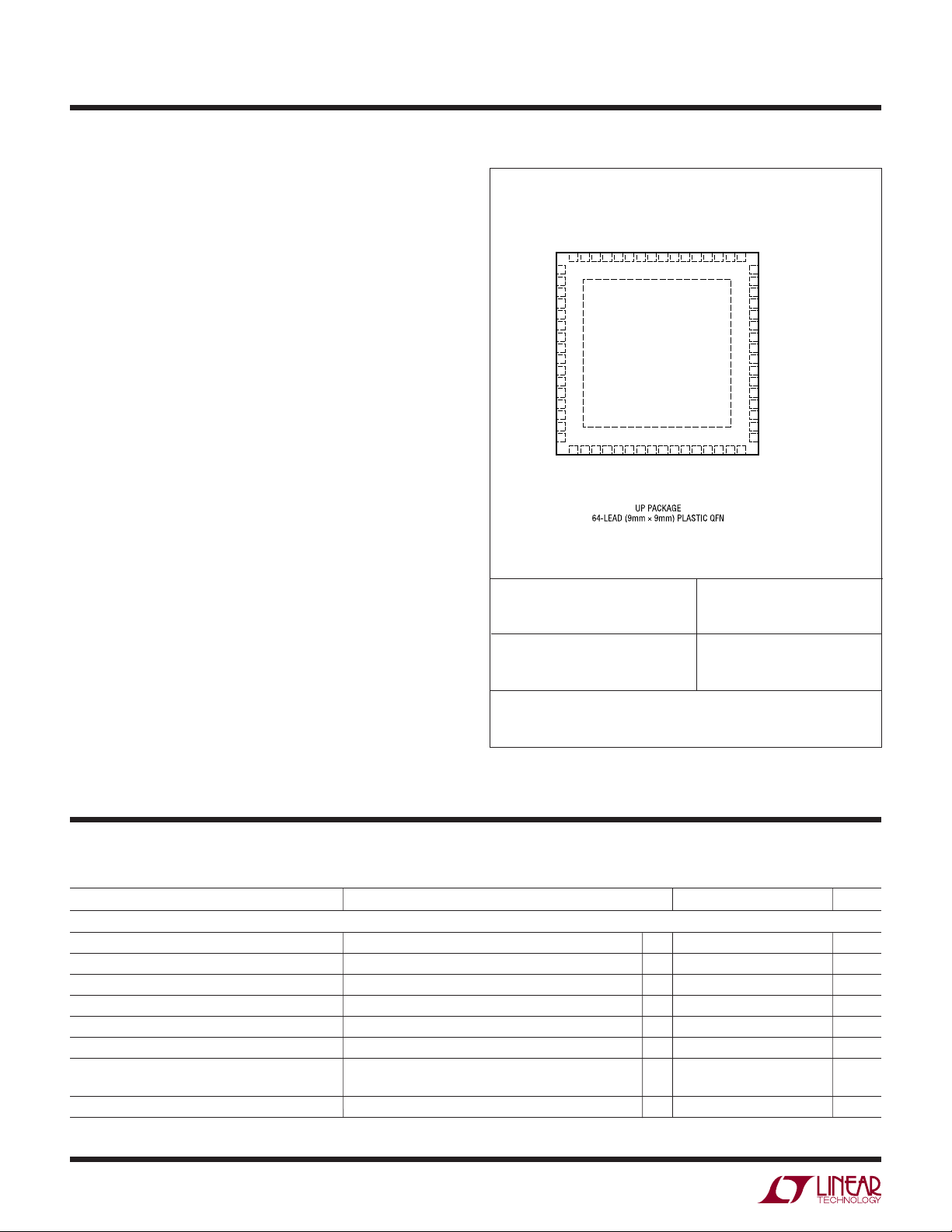
64-Pin (9mm × 9mm) QFN Package
U
APPLICATIO S
■
Telecommunications
■
Receivers
■
Cellular Base Stations
■
Spectrum Analysis
■
Imaging Systems
■
ATE
, LT, LTC and LTM are registered trademarks of Linear Technology Corporation.
All other trademarks are the property of their respective owners.
LTC2208
16-Bit, 130Msps ADC
U
DESCRIPTIO
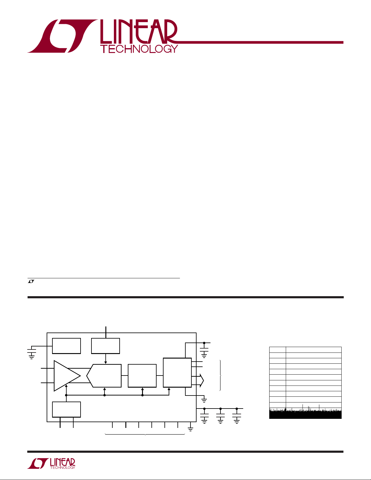
The LTC®2208 is a 130Msps, sampling 16-bit A/D converter designed for digitizing high frequency, wide dynamic
range signals with input frequencies up to 700MHz. The
input range of the ADC can be optimized with the PGA
front end.
The LTC2208 is perfect for demanding communications
applications, with AC performance that includes 78dBFS
Noise Floor and 100dB spurious free dynamic range
(SFDR). Ultra low jitter of 70fs
of high input frequencies with excellent noise performance.
Maximum DC specs include ±4LSB INL, ±1LSB DNL (no
missing codes).
The digital output can be either differential LVDS or
single-ended CMOS. There are two format options for the
CMOS outputs: a single bus running at the full data rate or
demultiplexed buses running at half data rate. A separate
output power supply allows the CMOS output swing to
range from 0.5V to 3.6V.
+
The ENC
and ENC– inputs may be driven differentially
or single-ended with a sine wave, PECL, LVDS, TTL or
CMOS inputs. An optional clock duty cycle stabilizer allows high performance at full speed with a wide range of
clock duty cycles.
allows undersampling
RMS
TYPICAL APPLICATIO
3.3V
SENSE
–
INTERNAL ADC
REFERENCE
GENERATOR
16-BIT
PIPELINED
ADC CORE
PGA SHDN DITH MODE LVDS RAND
ANALOG
INPUT
V
CM
2.2µF
AIN
AIN
COMMON MODE
+
–
1.25V
BIAS VOLTAGE
+
S/H
AMP
–
CLOCK/DUTY
CYCLE
CONTROL
+
ENC
ENC
U
CORRECTION
LOGIC AND
SHIFT REGISTER
ADC CONTROL INPUTS
OUTPUT
DRIVERS
OV
DD
OGND
V
GND
64k Point FFT, FIN = 15.1MHz,
0.5V TO 3.6V
1µF
OF
CLKOUT
D15
DD
CMOS
OR
•
LVDS
•
•
D0
1µF 1µF 1µF
3.3V
2208 TA01
0
–10
–20
–30
–40
–50
–60
–70
–80
AMPLITUDE (dBFS)
–90
–100
–110
–120
–130
0
–1dB, PGA = 0
20
10
FREQUENCY (MHz)
50
40
30
60
2208 G03
2208fb
1
LTC2208
WW
W
U
ABSOLUTE AXI U RATI GS
OV
= VDD (Notes 1 and 2)
DD
Supply Voltage (VDD) ...................................–0.3V to 4V
Digital Output Ground Voltage (OGND) ........–0.3V to 1V
Analog Input Voltage (Note 3) ..... –0.3V to (V
Digital Input Voltage .................... –0.3V to (V
Digital Output Voltage ................ –0.3V to (OV
Power Dissipation ............................................ 2000mW
Operating Temperature Range
LTC2208C ................................................0°C to 70°C
LTC2208I .............................................– 40°C to 85°C
Storage Temperature Range ..................–65°C to 150°C
Digital Output Supply Voltage (OV
) .......... –0.3V to 4V
DD
+ 0.3V)
DD
+ 0.3V)
DD
+ 0.3V)
DD
SENSE 1
GND 2
V
CM
GND 4
V
DD
V
DD
GND 7
AIN
AIN
GND 10
GND 11
+
ENC
–
ENC
GND 14
V
DD
V
DD
TOP VIEW
/DA14
+
/OFA
/DA15
+
–
59 OF
64 PGA
63 RAND
3
5
6
+
8
–
9
12
13
15
16
17
DD
V
GND 18
EXPOSED PAD IS GND (PIN 65)
MUST BE SOLDERED TO PCB BOARD
T
58 D15
62 MODE
61 LVDS
60 OF
19
20
/DB0 21
/DB1 22
/DB2 23
DITH
SHDN
–
+
–
D0
D1
DO
= 125°C, θJA = 20°C/W**
JMAX
+
–
57 D15 /DA13
65
/DB3 24
+
–
D1
/DA12
/DA11
–
56 D14
55 D14
/DB4 25
/DB5 26
+
D2
D2
/DA10
+
–
54 D13
/DB6 27
–
+
D3
/DA9
53 D13
/DB7 28
D3
UUW
FOR ATIOPACKAGE/ORDER I
/DA8
–
+
DD
52 D12
51 D12 /DA7
50 OGND
49 OV
48 D11
47 D11
46 D10
45 D10
+
44 D9
–
43 D9
+
42 D8
–
41 D8
40 CLKOUT
39 CLKOUT
+
38 D7
–
37 D7
+
36 D6
–
35 D6
+
34 D5
–
33 D5
32
DD
/DB8 29
/DB9 30
–
+
OV
OGND 31
D4
D4
+
/DA6
–
/DA5
+
/DA4
–
/DA3
/DA2
/DA1
/DA0
/CLKOUTA
+
/CLKOUTB
–
/OFB
/DB15
/DB14
/DB13
/DB12
/DB11
/DB10
ORDER PART
NUMBER
LTC2208CUP
UP PART
MARKING*
LTC2208UP
LTC2208IUP
Order Options Tape and Reel: Add #TR
Lead Free: Add #PBF Lead Free Tape and Reel: Add #TRPBF
Lead Free Part Marking: http://www.linear.com/leadfree/
Consult LTC Marketing for parts specifi ed with wider operating temperature ranges.
*The temperature grade is identifi ed by a label on the shipping container.
= 150°C, option available, consult factory.
**T
JMAX
U
CO VERTER CHARACTERISTICS
The
temperature range, otherwise specifi cations are at T
PARAMETER CONDITIONS MIN TYP MAX UNITS
Integral Linearity Error Differential Analog Input (Note 5) TA = 25°C ±1.2 ±4.0 LSB
Integral Linearity Error Differential Analog Input (Note 5)
Differential Linearity Error Differential Analog Input
Offset Error (Note 6)
Offset Drift ±10 μV/
Gain Error External Reference
Full-Scale Drift Internal Reference ±30
Transition Noise External Reference 2.9 LSB
= 25°C. (Note 4)
A
External Reference ±15
●
denotes the specifi cations which apply over the full operating
●
±1.5 ±4.5 LSB
●
±0.3 ±1 LSB
●
±2 ±8.5 mV
●
±0.2 ±1.5 %FS
ppm/°C
ppm/°C
RMS
°C
2
2208fb
LTC2208
T
UU
A ALOG I PU
The
specifi cations are at T
SYMBOL PARAMETER CONDITIONS MIN TYP MAX UNITS
VIN Analog Input Range (A
V
IN, CM
I
Analog Input Leakage Current 0V ≤ A
IN
I
SENSE Input Leakage Current 0V ≤ SENSE ≤ VDD
SENSE
MODE Pin Pull-Down Current to GND 10 µA
I
MODE
I
LVDS Pin Pull-Down Current to GND 10 µA
LVDS
C
Analog Input Capacitance Sample Mode ENC+ < ENC– 6.5 pF
IN
Hold Mode ENC
t
Sample-and-Hold 1 ns
AP
Acquisition Delay Time
t
Sample-and-Hold 70 fs RMS
JITTER
Acquisition Delay Time Jitter
CMRR Analog Input 1V < (A
Common Mode Rejection Ratio
BW-3dB Full Power Bandwidth R
U
W
DY A IC ACCURACY
The
= 25°C. (Note 4)
A
Analog Input Common Mode Differential Input (Note 7)
otherwise specifi cations are at T
SYMBOL PARAMETER CONDITIONS MIN TYP MAX UNITS
SNR Signal-to-Noise Ratio 5MHz Input (2.25V Range, PGA = 0) 77.7 dBFS
5MHz Input (1.5V Range, PGA = 1) 75.3 dBFS
30MHz Input (2.25V Range, PGA = 0) T
30MHz Input (2.25V Range, PGA = 0)
30MHz Input (1.5V Range, PGA = 1) 75.2 dBFS
70MHz Input (2.25V Range, PGA = 0) 77.5 dBFS
70MHz Input (1.5V Range, PGA = 1) 75.1 dBFS
140MHz Input (2.25V Range, PGA = 0) 76.9 dBFS
140MHz Input (1.5V Range, PGA = 1) T
140MHz Input (1.5V Range, PGA = 1)
250MHz Input (2.25V Range, PGA = 0) 75.4 dBFS
250MHz Input (1.5V Range, PGA =1 ) 73.8 dBFS
SFDR Spurious Free 5MHz Input (2.25V Range, PGA = 0) 100 dBc
Dynamic Range 5MHz Input (1.5V Range, PGA = 1) 100 dBc
2
30MHz Input (2.25V Range, PGA = 0)
30MHz Input (1.5V Range, PGA = 1) 100 dBc
70MHz Input (2.25V Range, PGA = 0) 90 dBc
70MHz Input (1.5V Range, PGA = 1) 95 dBc
140MHz Input (2.25V Range, PGA = 0) 85 dBc
140MHz Input (1.5V Range, PGA = 1) T
140MHz Input (1.5V Range, PGA = 1)
250MHz Input (2.25V Range, PGA = 0) 78 dBc
250MHz Input (1.5V Range, PGA = 1)
nd
or 3rd Harmonic 30MHz Input (2.25V Range, PGA = 0) TA = 25°C 88 95 dBc
●
denotes the specifi cations which apply over the full operating temperature range, otherwise
+
–
– A
IN
= 25°C. AIN = –1dBFS. (Note 4)
A
) 3.135V ≤ V
IN
< 25Ω 700 MHz
S
●
denotes the specifi cations which apply over the full operating temperature range,
≤ 3.465V 1.5 or 2.25 V
DD
●
+
–
, A
≤ VDD
IN
IN
+
–
> ENC
+
–
= A
IN
) <1.5V 80 dB
IN
= 25°C 76.5 77.6 dBFS
A
= 25°C 73.8 74.8 dBFS
A
= 25°C 86 90 dBc
A
1 1.25 1.5 V
●
–1 1 µA
●
–3 3 µA
1.8 pF
●
76.1 77.3 dBFS
●
73.4 74.5 dBFS
●
87 94 dBc
●
84 89 dBc
83 dBc
P-P
2208fb
3
LTC2208
U
W
DY A IC ACCURACY
The
otherwise specifi cations are at T
SYMBOL PARAMETER CONDITIONS MIN TYP MAX UNITS
SFDR Spurious Free 5MHz Input (2.25V Range, PGA = 0) 100 dBc
Dynamic Range 5MHz Input (1.5V Range, PGA = 1) 100 dBc
4
or Higher 30MHz Input (1.5V Range, PGA = 1) 100 dBc
70MHz Input (2.25V Range, PGA = 0) 100 dBc
70MHz Input (1.5V Range, PGA = 1) 100 dBc
140MHz Input (2.25V Range, PGA = 0) 95 dBc
140MHz Input (1.5V Range, PGA = 1)
250MHz Input (2.25V Range, PGA = 0) 90 dBc
250MHz Input (1.5V Range, PGA = 1)
S/(N+D) Signal-to-Noise 5MHz Input (2.25V Range, PGA = 0) 77.7 dBFS
Plus Distortion Ratio 5MHz Input (1.5V Range, PGA = 1) 75.3 dBFS
30MHz Input (2.25V Range, PGA = 0) T
30MHz Input (2.25V Range, PGA = 0)
30MHz Input (1.5V Range, PGA = 1) 75.2 dBFS
70MHz Input (2.25V Range, PGA = 0) 77.4 dBFS
70MHz Input (1.5V Range, PGA = 1) 75 dBFS
140MHz Input (2.25V Range, PGA = 0) 76.4 dBFS
140MHz Input (1.5V Range, PGA = 1) T
140MHz Input (1.5V Range, PGA = 1)
250MHz Input (2.25V Range, PGA = 0) 73.6 dBFS
250MHz Input (1.5V Range, PGA = 1)
SFDR Spurious Free Dynamic Range 5MHz Input (2.25V Range, PGA = 0) 105 dBFS
at –25dBFS 5MHz Input (1.5V Range, PGA = 1) 105 dBFS
Dither “OFF” 30MHz Input (2.25V Range, PGA = 0) 105 dBFS
30MHz Input (1.5V Range, PGA = 1) 105 dBFS
70MHz Input (2.25V Range, PGA = 0) 105 dBFS
70MHz Input (1.5V Range, PGA = 1) 105 dBFS
14 0MHz Input (2.25V Range, PGA = 0) 100 dBFS
140MHz Input (1.5V Range, PGA = 1)
250MHz Input (2.25V Range, PGA = 0) 100 dBFS
250MHz Input (1.5V Range, PGA = 1)
SFDR Spurious Free Dynamic Range 5MHz Input (2.25V Range, PGA = 0) 115 dBFS
at –25dBFS 5MHz Input (1.5V Range, PGA = 1) 115 dBFS
Dither “ON” 30MHz Input (2.25V Range, PGA = 0)
30MHz Input (1.5V Range, PGA = 1) 115 dBFS
70MHz Input (2.25V Range, PGA = 0) 115 dBFS
70MHz Input (1.5V Range, PGA = 1) 115 dBFS
140MHz Input (2.25V Range, PGA = 0) 110 dBFS
140MHz Input (1.5V Range, PGA = 1)
250MHz Input (2.25V Range, PGA = 0) 105 dBFS
250MHz Input (1.5V Range, PGA = 1)
th
Harmonic 30MHz Input (2.25V Range, PGA = 0)
= 25°C. AIN = –1dBFS unless otherwise noted. (Note 4)
A
●
denotes the specifi cations which apply over the full operating temperature range,
●
90 100 dBc
●
88 95 dBc
90 dBc
= 25°C 76.3 77.5 dBFS
A
= 25°C 73.6 74.5 dBFS
A
●
75.9 77.5 dBFS
●
73.2 74.5 dBFS
72.9 dBFS
100 dBFS
100 dBFS
●
100 115 dBFS
110 dBFS
105 dBFS
4
2208fb
LTC2208
WW
CO O ODE BIAS CHARACTERISTICS
The ● denotes the specifi cations which apply over
the full operating temperature range, otherwise specifi cations are at T
PARAMETER CONDITIONS MIN TYP MAX UNITS
VCM Output Voltage I
VCM Output Tempco I
VCM Line Regulation 3.135V ≤ V
V
Output Resistance 1mA ≤ | I
CM
U
W
= 25°C. (Note 4)
A
= 0 1.15 1.25 1.35 V
OUT
= 0 +40
OUT
≤ 3.465V 1 mV/ V
DD
| ≤ 1mA 2 Ω
OUT
ppm/°C
UU
DIGITAL I PUTS A D DIGITAL OUTPUTS
The
full operating temperature range, otherwise specifi cations are at T
SYMBOL PARAMETER CONDITIONS MIN TYP MAX UNITS
ENCODE INPUTS (ENC+, ENC–)
VID Differential Input Voltage (Note 7) ● 0.2 V
V
ICM
Externally Set (Note 7) 1.2 3.0 V
R
Input Resistance (See Figure 2) 6 kΩ
IN
CIN Input Capacitance (Note 7) 3 pF
LOGIC INPUTS (DITH, PGA, SHDN, RAND)
VIH High Level Input Voltage VDD = 3.3V
VIL Low Level Input Voltage V
IIN Digital Input Current VIN = 0V to VDD ● ±10 µA
C
IN
LOGIC OUTPUTS (CMOS MODE)
OV
= 3.3V
DD
VOH High Level Output Voltage VDD = 3.3V IO = –10µA 3.299 V
I
VOL Low Level Output Voltage VDD = 3.3V IO = 160µA 0.01 V
I
I
SOURCE
I
SINK
OVDD = 2.5V
VOH High Level Output Voltage VDD = 3.3V IO = –200µA 2.49 V
Low Level Output Voltage VDD = 3.3V IO = 1.60mA 0.1 V
V
OL
OVDD = 1.8V
VOH High Level Output Voltage VDD = 3.3V IO = –200µA 1.79 V
VOL Low Level Output Voltage VDD = 3.3V IO = 1.60mA 0.1 V
LOGIC OUTPUTS (LVDS MODE)
STANDARD LVDS
VOD Differential Output Voltage 100Ω Differential Load
VOS Output Common Mode Voltage 100Ω Differential Load
LOW POWER LVDS
VOD Differential Ouptut Voltage 100Ω Differential Load
VOS Output Common Mode Voltage 100Ω Differential Load
Common Mode Input Voltage Internally Set 1.6 V
= 3.3V
DD
Digital Input Capacitance
Output Source Current
Output Sink Current
(Note 7) 1.5 pF
V
OUT
V
OUT
= 25°C. (Note 4)
A
= 0V – 50 mA
= 3.3V 50 mA
●
denotes the specifi cations which apply over the
●
2 V
●
0.8 V
= –200µA ● 3.1 3.29 V
O
= 1.6mA ● 0.10 0.4 V
O
●
247 350 454 mV
●
1.125 1.2 1.375 V
●
125 175 250 mV
●
1.125 1.2 1.375 V
2208fb
5
LTC2208
WU
POWER REQUIRE E TS
The
range, otherwise specifi cations are at T
SYMBOL PARAMETER CONDITIONS MIN TYP MAX UNITS
V
DD
P
Shutdown Power SHDN = VDD 0.2 mW
SHDN
STANDARD LVDS OUTPUT MODE
OVDD Output Supply Voltage (Note 8)
I
Analog Supply Current
VDD
I
Output Supply Current
OVDD
P
Power Dissipation
DIS
LOW POWER LVDS OUTPUT MODE
OVDD Output Supply Voltage (Note 8)
I
Analog Supply Current
VDD
I
Output Supply Current
OVDD
P
Power Dissipation
DIS
CMOS OUTPUT MODE
OVDD Output Supply Voltage (Note 8)
I
Analog Supply Current
VDD
P
Power Dissipation
DIS
Analog Supply Voltage (Note 8)
= 25°C. AIN = –1dBFS. (Note 4)
A
●
denotes the specifi cations which apply over the full operating temperature
●
3.135 3.3 3.465 V
●
3 3.3 3.6 V
●
380 450 mA
●
74 90 mA
●
1498 1782 mW
●
3 3.3 3.6 V
●
380 450 mA
●
31 50 mA
●
1356 1650 mW
●
0.5 3.6 V
●
380 450 mA
●
1250 1485 mW
UW
TI I G CHARACTERISTICS
The
range, otherwise specifi cations are at T
SYMBOL PARAMETER CONDITIONS MIN TYP MAX UNITS
fS Sampling Frequency (Note 8)
tL ENC Low Time Duty Cycle Stabilizer Off (Note 7)
Duty Cycle Stabilizer On (Note 7)
tH ENC High Time Duty Cycle Stabilizer Off (Note 7)
Duty Cycle Stabilizer On (Note 7)
tAP Sample-and-Hold Aperture Delay –1 ns
LVDS OUTPUT MODE (STANDARD and LOW POWER)
tD ENC to DATA Delay (Note 7)
t
ENC to CLKOUT Delay (Note 7)
C
t
DATA to CLKOUT Skew (tC-tD) (Note 7)
SKEW
t
Output Rise Time 0.5 ns
RISE
t
Output Fall Time 0.5 ns
FALL
Data Latency Data Latency 7 Cycles
CMOS OUTPUT MODE
tD ENC to DATA Delay (Note 7)
tC ENC to CLKOUT Delay (Note 7)
t
DATA to CLKOUT Skew (tC-tD) (Note 7)
SKEW
Data Latency Data Latency Full Rate CMOS 7 Cycles
Demuxed 7 Cycles
= 25°C. (Note 4)
A
●
denotes the specifi cations which apply over the full operating temperature
●
1 130 MHz
●
3.65 3.846 1000 ns
●
2.6 3.846 1000 ns
●
3.65 3.846 1000 ns
●
2.6 3.846 1000 ns
●
1.3 2.5 3.8 ns
●
1.3 2.5 3.8 ns
●
–0.6 0 0.6 ns
●
1.3 2.7 4.0 ns
●
1.3 2.7 4.0 ns
●
–0.6 0 0.6 ns
6
2208fb
ELECTRICAL CHARACTERISTICS
LTC2208
Note 1: Stresses beyond those listed under Absolute Maximum Ratings
may cause permanent damage to the device. Exposure to any Absolute
Maximum Rating condition for extended periods may affect device
reliability and lifetime.
Note 2: All voltage values are with respect to GND, with GND and OGND
shorted (unless otherwise noted).
Note 3: When these pin voltages are taken below GND or above V
DD
, they
will be clamped by internal diodes. This product can handle input currents
of greater than 100mA below GND or above V
Note 4: V
ENC
–
= 2V
= 3.3V, f
DD
sine wave with 1.6V common mode, input range = 2.25V
P-P
= 130MHz, LVDS outputs, differential ENC+/
SAMPLE
without latchup.
DD
P-P
with differential drive (PGA = 0), unless otherwise specifi ed.
UWW
TI I G DIAGRA
LVDS Output Mode Timing
All Outputs are Differential and Have LVDS Levels
t
ANALOG
INPUT
ENC
ENC
D0-D15, OF
AP
N
t
H
–
+
t
D
N + 1
t
L
N – 7 N – 6 N – 5 N – 4 N – 3
Note 5: Integral nonlinearity is defi ned as the deviation of a code from a “best
fi t straight line” to the transfer curve. The deviation is measured from the
center of the quantization band.
Note 6: Offset error is the offset voltage measured from –1/2LSB when the
output code fl ickers between 0000 0000 0000 0000 and 1111 1111 1111
1111 in 2’s complement output mode.
Note 7: Guaranteed by design, not subject to test.
Note 8: Recommended operating conditions.
N + 4
N + 2
N + 3
CLKOUT
CLKOUT
t
+
–
C
2208 TD01
2208fb
7
LTC2208
3
WUW
TI I G DIAGRA S
ANALOG
INPUT
–
ENC
+
ENC
DA0-DA15, OFA
CLKOUTA
CLKOUTB
Full-Rate CMOS Output Mode Timing
All Outputs are Single-Ended and Have CMOS Levels
t
AP
N
t
H
t
D
t
C
N + 1
N + 2
t
L
N – 7 N – 6 N – 5 N – 4 N – 3
N + 3
N + 4
DB0-DB15, OFB
ANALOG
INPUT
ENC
ENC
DA0-DA15, OFA
DB0-DB15, OFB
CLKOUTA
CLKOUTB
HIGH IMPEDANCE
2208 TD02
Demultiplexed CMOS Output Mode Timing
All Outputs are Single-Ended and Have CMOS Levels
t
AP
N
t
H
–
+
t
D
t
D
t
C
N + 1
N + 2
t
L
N – 8 N – 6 N – 4
N – 7 N – 5 N – 3
N + 3
N + 4
2208 TD0
8
2208fb
TYPICAL PERFOR
LTC2208
UW
CE CHARACTERISTICSA
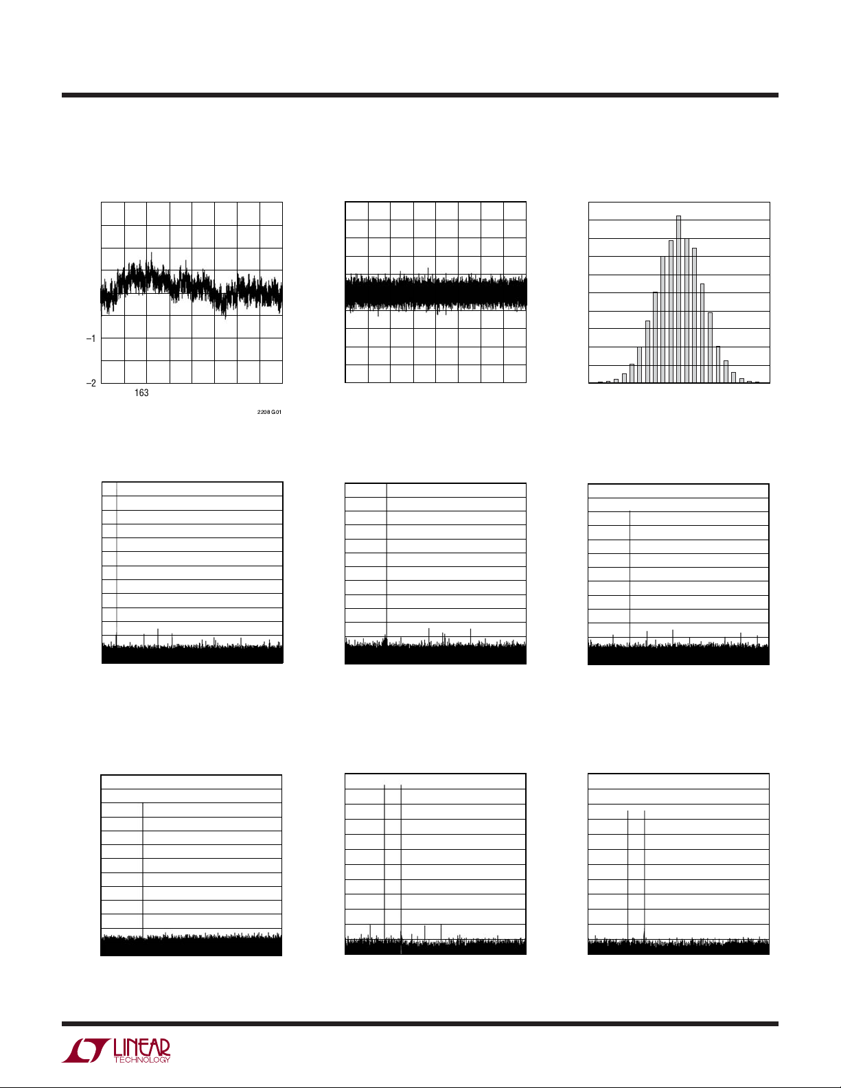
Integral Nonlinearity (INL) vs
Output Code
2
1.5
1
0.5
0
–0.5
INL ERROR (LSB)
–1
–1.5
–2
0
16384
128K Point FFT, f
32768
OUTPUT CODE
IN
–1dBFS, PGA = 0
0
–10
–20
–30
–40
–50
–60
–70
–80
AMPLITUDE (dBFS)
–90
–100
–110
–120
–130
10
0
30
20
FREQUENCY (MHz)
49152
& /
= 4.93MHz,
40
50
65536
60
2208 G15
Differential Nonlinearity (DNL) vs
Output Code
1
0.8
0.6
0.4
0.2
0
0.2
DNL ERROR (LSB)
0.4
0.6
0.8
1
0
16384
32768
OUTPUT CODE
64k Point FFT, fIN = 15.1MHz,
–1dBFS, PGA = 0
0
–10
–20
–30
–40
–50
–60
–70
–80
AMPLITUDE (dBFS)
–90
–100
–110
–120
–130
0
20
10
FREQUENCY (MHz)
40
30
49152
50
2208 G02
60
2208 G03
65536
AC Grounded Input Histogram
10000
9000
8000
7000
6000
5000
COUNT
4000
3000
2000
1000
0
32736 32740 32744 32748 32752 32756
OUTPUT CODE
64k Point FFT, 15.1MHz, –20dBFS,
PGA = 0, Internal Dither “Off”
0
–10
–20
–30
–40
–50
–60
–70
–80
AMPLITUDE (dBFS)
–90
–100
–110
–120
–130
0
20
10
FREQUENCY (MHz)
40
30
2208 G14
50
60
2208 G04
64k Point FFT, 15.1MHz, –20dBFS,
PGA = 0, Internal Dither “On”
0
–10
–20
–30
–40
–50
–60
–70
–80
AMPLITUDE (dBFS)
–90
–100
–110
–120
–130
0
20
10
FREQUENCY (MHz)
40
30
32k Point 2-Tone FFT,
= 21.14 MHz and 14.25MHz,
f
IN
–7dBFS, PGA = 0
0
–10
–20
–30
–40
–50
–60
–70
–80
AMPLITUDE (dBFS)
–90
–100
–110
–120
50
60
2208 G05
0
20
10
FREQUENCY (MHz)
30
50
40
60
2208 G06
32k Point 2-Tone FFT,
= 20.14 MHz and 14.25MHz,
f
IN
–25dBFS, PGA = 0
0
–10
–20
–30
–40
–50
–60
–70
–80
AMPLITUDE (dBFS)
–90
–100
–110
–120
0
20
10
FREQUENCY (MHz)
30
50
40
60
2208 G07
2208fb
9
LTC2208
UW
TYPICAL PERFOR A CE CHARACTERISTICS
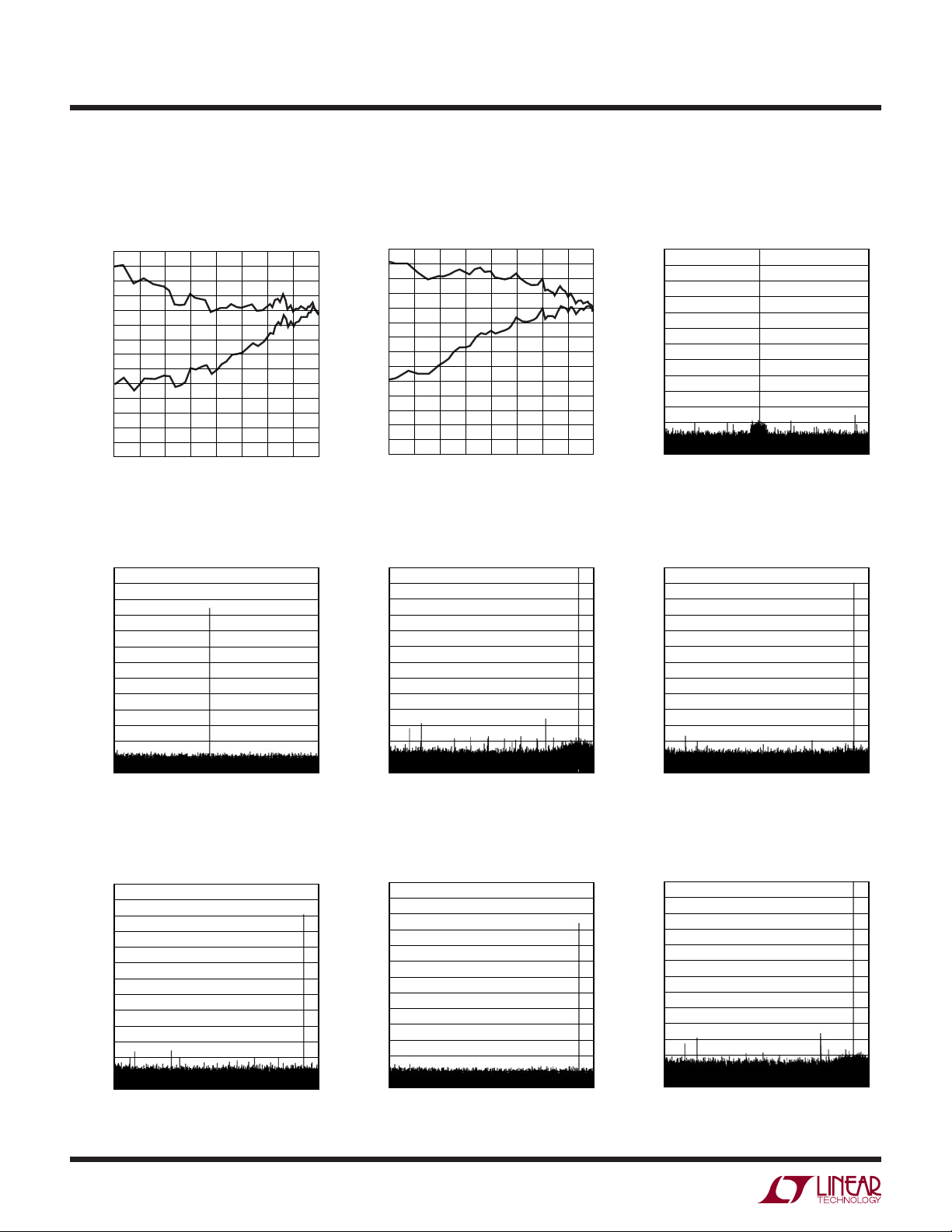
SFDR vs Input Level, fIN = 15MHz,
PGA = 0, Dither “Off”
140
130
120
110
100
90
80
70
60
50
40
SFDR (dBc AND dBFS)
30
20
10
0
–80
–60
–70
INPUT LEVEL (dBFS)
–50
–30
–40 0
128K Point FFT, fIN = 30.1 MHz,
–25dBFS, PGA = 0, Dither “On”
0
–10
–20
–30
–40
–50
–60
–70
–80
AMPLITUDE (dBFS)
–90
–100
–110
–120
–130
10
0
20
FREQUENCY (MHz)
40
30
–20 –10
50
2208 G08
60
2208 G17
SFDR vs Input Level, fIN = 15MHz,
PGA = 0, Dither “On”
140
130
120
110
100
90
80
70
60
50
40
SFDR (dBc AND dBFS)
30
20
10
0
–80
–60
–70
INPUT LEVEL (dBFS)
–50
–30
–40 0
64K Point FFT, fIN = 70.1 MHz,
–1dBFS, PGA = 0
0
–10
–20
–30
–40
–50
–60
–70
–80
AMPLITUDE (dBFS)
–90
–100
–110
–120
–130
10
0
20
FREQUENCY (MHz)
40
30
–20 –10
50
2208 G09
60
2208 G18
64K Point FFT, f
= 30.1 MHz,
IN
–1dBFS, PGA = 0
0
–10
–20
–30
–40
–50
–60
–70
–80
AMPLITUDE (dBFS)
–90
–100
–110
–120
–130
10
0
30
20
FREQUENCY (MHz)
64K Point FFT, fIN = 70.1 MHz,
–10dBFS, PGA = 0
0
–10
–20
–30
–40
–50
–60
–70
–80
AMPLITUDE (dBFS)
–90
–100
–110
–120
–130
10
0
30
20
FREQUENCY (MHz)
40
50
60
2208 G16
40
50
60
2208 G19
64K Point FFT, fIN = 70.1 MHz,
–20dBFS, PGA = 0
0
–10
–20
–30
–40
–50
–60
–70
–80
AMPLITUDE (dBFS)
–90
–100
–110
–120
–130
10
0
30
20
FREQUENCY (MHz)
10
128K Point FFT, fIN = 70.1 MHz,
–25dBFS, PGA = 0, Dither “On”
0
–10
–20
–30
–40
–50
–60
–70
–80
AMPLITUDE (dBFS)
–90
–100
–110
–120
40
50
60
2208 G20
–130
10
0
20
FREQUENCY (MHz)
40
30
50
60
2208 G21
64K Point FFT, fIN = 70.1 MHz,
–1dBFS, PGA = 1
0
–10
–20
–30
–40
–50
–60
–70
–80
AMPLITUDE (dBFS)
–90
–100
–110
–120
–130
10
0
30
20
FREQUENCY (MHz)
40
50
60
2208 G22
2208fb
 Loading...