

FEATURES
LTC2053/LTC2053-SYNC
Precision, Rail-to-Rail,
Zero-Drift, Resistor-Programmable
Instrumentation Amplifier
U
DESCRIPTIO
■
116dB CMRR Independent of Gain
■
Maximum Offset Voltage: 10µV
■
Maximum Offset Voltage Drift: 50nV/°C
■
Rail-to-Rail Input
■
Rail-to-Rail Output
■
2-Resistor Programmable Gain
■
Supply Operation: 2.7V to ±5.5V
■
Typical Noise: 2.5µV
■
Typical Supply Current: 750µA
■
LTC2053-SYNC Allows Synchronization to
(0.01Hz to 10Hz)
P-P
External Clock
■
Available in MS8 and 3mm × 3mm × 0.8mm
DFN Packages
U
APPLICATIO S
■
Thermocouple Amplifiers
■
Electronic Scales
■
Medical Instrumentation
■
Strain Gauge Amplifiers
■
High Resolution Data Acquisition
The LTC®2053 is a high precision instrumentation amplifier. The CMRR is typically 116dB with a single or dual 5V
supply and is independent of gain. The input offset voltage
is guaranteed below 10µV with a temperature drift of less
than 50nV/°C. The LTC2053 is easy to use; the gain is
adjustable with two external resistors, like a traditional
op amp.
The LTC2053 uses charge balanced sampled data techniques to convert a differential input voltage into a single
ended signal that is in turn amplified by a zero-drift
operational amplifier.
The differential inputs operate from rail-to-rail and the
single ended output swings from rail-to-rail. The LTC2053
can be used in single supply applications, as low as 2.7V.
It can also be used with dual ±5.5V supplies. The LTC2053
requires no external clock, while the LTC2053-SYNC has
a CLK pin to synchronize to an external clock.
The LTC2053 is available in an MS8 surface mount package. For space limited applications, the LTC2053 is available in a 3mm × 3mm × 0.8mm dual fine pitch leadless
package (DFN).
, LTC and LT are registered trademarks of Linear Technology Corporation.
All other trademarks are the property of their respective owners.
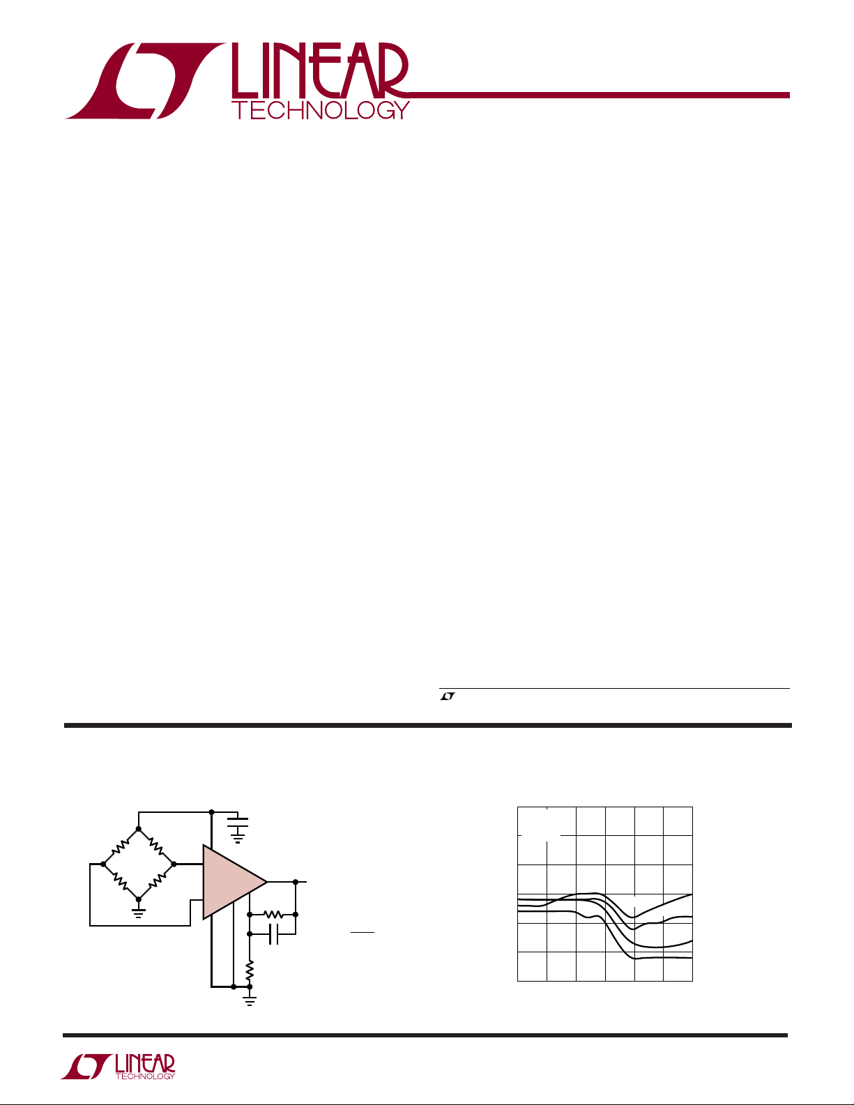
TYPICAL APPLICATIO
Differential Bridge Amplifier
3V
0.1µF
R < 10k
2
3
8
–
LTC2053
+
1, 4
6
R2 10k
5
R1
10Ω
7
0.1µF
U
OUT
GAIN = 1+
2053 TA01
Typical Input Referred Offset vs Input
Common Mode Voltage (VS = 3V)
15
VS = 3V
= 0V
V
REF
= 25°C
T
10
A
5
0
R2
R1
–5
INPUT OFFSET VOLTAGE (µV)
–10
–15
0
1.0 1.5 2.0
0.5
INPUT COMMON MODE VOLTAGE (V)
G = 1000
G = 10
G = 100
G = 1
2.5 3.0
2053 TA01b
2053syncfb
1
LTC2053/LTC2053-SYNC
WW
W
U
ABSOLUTE AXI U RATI GS
(Note 1)
Total Supply Voltage (V+ to V–) ............................... 11V
Input Current ...................................................... ±10mA
+
⏐V
⏐V
IN
IN
– V
–
– V
⏐ ........................................................ 5.5V
REF
⏐ ........................................................ 5.5V
REF
Output Short Circuit Duration .......................... Indefinite
Operating Temperature Range
LTC2053C, LTC2053C-SYNC................... 0°C to 70°C
UUW
PACKAGE/ORDER I FOR ATIO
ORDER PART NUMBER
LTC2053CMS8
†
EN/CLK
1
2
–IN
3
+IN
–
4
V
MS8 PACKAGE
8-LEAD PLASTIC MSOP
T
= 150°C, θJA = 200°C/W
JMAX
†
PIN 1 IS EN ON LTC2053,
CLK ON LTC2053-SYNC
TOP VIEW
+
8
V
7
OUT
6
RG
5
REF
LTC2053IMS8
LTC2053HMS8
LTC2053CMS8-SYNC
LTC2053IMS8-SYNC
MS8 PART MARKING
LTVT
LTJY
LTAFB
LTC2053I, LTC2053I-SYNC ................ – 40°C to 85°C
LTC2053H ........................................ –40°C to 125°C
Storage Temperature Range
MS8 Package ................................... – 65°C to 150°C
DD Package ...................................... –65°C to 125°C
Lead Temperature (Soldering, 10 sec).................. 300°C
TOP VIEW
+
1
EN
–IN
2
+IN
3
–
V
4
8-LEAD (3mm × 3mm) PLASTIC DFN
DD PACKAGE
T
= 125°C, θJA = 160°C/W
JMAX
UNDERSIDE METAL INTERNALLY
CONNECTED TO V
(PCB CONNECTION OPTIONAL)
8
V
OUT
7
RG
6
REF
5
–
ORDER PART NUMBER
LTC2053CDD
LTC2053IDD
LTC2053HDD
DD PART MARKING
*LAEQ
*LTBNP
*The temperature grade (C, I, or H) is indicated on the shipping container. Consult LTC Marketing for parts specified with wider operating temperature ranges.
ELECTRICAL CHARACTERISTICS
temperature range, otherwise specifications are at TA = 25°C. V+ = 3V, V– = 0V, REF = 200mV. Output voltage swing is referenced
to V–. All other specifications reference the OUT pin to the REF pin.
PARAMETER CONDITIONS MIN TYP MAX UNITS
Gain Error AV = 1 ● 0.001 0.01 %
Gain Nonlinearity AV = 1, LTC2053 ● 3 12 ppm
= 1, LTC2053-SYNC ● 3 15 ppm
A
V
Input Offset Voltage (Note 2) VCM = 200mV –5 ±10 µV
Average Input Offset Drift (Note 2) TA = –40°C to 85°C ● ±50 nV/°C
= 85°C to 125°C ● –1 –2.5 µV/°C
T
A
Average Input Bias Current (Note 3) VCM = 1.2V ● 410 nA
Average Input Offset Current (Note 3) VCM = 1.2V ● 13 nA
Input Noise Voltage DC to 10Hz 2.5 µV
Common Mode Rejection Ratio AV = 1, VCM = 0V to 3V, LTC2053C, LTC2053C-SYNC ● 100 113 dB
(Notes 4, 5) A
= 1, VCM = 0.1V to 2.9V, LTC2053I, LTC2053I-SYNC ● 100 113 dB
V
A
= 1, VCM = 0V to 3V, LTC2053I, LTC2053I-SYNC ● 95 113 dB
V
= 1, VCM = 0.1V to 2.9V, LTC2053H ● 100 dB
A
V
= 1, VCM = 0V to 3V, LTC2053H ● 85 dB
A
V
The ● denotes the specifications which apply over the full operating
P-P
2053syncfb
2
LTC2053/LTC2053-SYNC
ELECTRICAL CHARACTERISTICS
temperature range, otherwise specifications are at T
–
to V
. All other specifications reference the OUT pin to the REF pin.
The ● denotes the specifications which apply over the full operating
= 25°C. V+ = 3V, V– = 0V, REF = 200mV. Output voltage swing is referenced
A
PARAMETER CONDITIONS MIN TYP MAX UNITS
Power Supply Rejection Ratio (Note 6) VS = 2.7V to 6V ● 110 116 dB
Output Voltage Swing High RL = 2k to V
= 10k to V
R
L
–
–
● 2.85 2.94 V
● 2.95 2.98 V
Output Voltage Swing Low ● 20 mV
Supply Current No Load ● 0.75 1 mA
Supply Current, Shutdown VEN ≥ 2.5V, LTC2053 Only 10 µA
EN/CLK Pin Input Low Voltage, V
EN/CLK Pin Input High Voltage, V
IL
IH
EN/CLK Pin Input Current V
EN/CLK
= V
2.5 V
–
–0.5 – 10 µA
0.5 V
Internal Op Amp Gain Bandwidth 200 kHz
Slew Rate 0.2 V/µs
Internal Sampling Frequency 3kHz
The ● denotes the specifications which apply over the full operating temperature range, otherwise specifications are at TA = 25°C. V+ = 5V,
V– = 0V, REF = 200mV. Output voltage swing is referenced to V–. All other specifications reference the OUT pin to the REF pin.
PARAMETER CONDITIONS MIN TYP MAX UNITS
Gain Error AV = 1 ● 0.001 0.01 %
Gain Nonlinearity AV = 1 ● 3 10 ppm
Input Offset Voltage (Note 2) VCM = 200mV –5 ±10 µV
Average Input Offset Drift (Note 2) TA = – 40°C to 85°C ● ±50 nV/°C
= 85°C to 125°C ● –1 –2.5 µV/°C
T
A
Average Input Bias Current (Note 3) VCM = 1.2V ● 410 nA
Average Input Offset Current (Note 3) VCM = 1.2V ● 13 nA
Common Mode Rejection Ratio AV = 1, VCM = 0V to 5V, LTC2053C ● 105 116 dB
(Notes 4, 5) A
Power Supply Rejection Ratio (Note 6) VS = 2.7V to 6V ● 110 116 dB
Output Voltage Swing High RL = 2k to V
Output Voltage Swing Low ● 20 mV
Supply Current No Load ● 0.85 1.1 mA
Supply Current, Shutdown VEN ≥ 4.5V, LTC2053 Only 10 µA
EN/CLK Pin Input Low Voltage, V
EN/CLK Pin Input High Voltage, V
IL
IH
EN/CLK Pin Input Current V
Internal Op Amp Gain Bandwidth 200 kHz
Slew Rate 0.2 V/µs
Internal Sampling Frequency 3kHz
= 1, VCM = 0V to 5V, LTC2053C-SYNC ● 100 116 dB
V
= 1, VCM = 0.1V to 4.9V, LTC2053I ● 105 116 dB
A
V
A
= 1, VCM = 0.1V to 4.9V, LTC2053I-SYNC ● 100 116 dB
V
= 1, VCM = 0V to 5V, LTC2053I, LTC2053I-SYNC ● 95 116 dB
A
V
= 1, VCM = 0.1V to 4.9V, LTC2053H ● 100 dB
A
V
A
= 1, VCM = 0V to 5V, LTC2053H ● 85 dB
V
= 10k to V
R
L
–
–
● 4.85 4.94 V
● 4.95 4.98 V
0.5 V
4.5 V
–
EN/CLK
= V
–1 –10 µA
2053syncfb
3
LTC2053/LTC2053-SYNC
ELECTRICAL CHARACTERISTICS
temperature range, otherwise specifications are at T
PARAMETER CONDITIONS MIN TYP MAX UNITS
Gain Error AV = 1 ● 0.001 0.01 %
Gain Nonlinearity AV = 1 ● 3 10 ppm
Input Offset Voltage (Note 2) VCM = 0V 10 ±20 µV
Average Input Offset Drift (Note 2) TA = –40°C to 85°C ● ±50 nV/°C
= 85°C to 125°C ● –1 –2.5 µV/°C
T
A
Average Input Bias Current (Note 3) VCM = 1V ● 410 nA
Average Input Offset Current (Note 3) VCM = 1V ● 13 nA
Common Mode Rejection Ratio AV = 1, VCM = – 5V to 5V, LTC2053C ● 105 118 dB
(Notes 4, 5) A
(Notes 4, 5) A
Power Supply Rejection Ratio (Note 6) VS = 2.7V to 11V ● 110 116 dB
Maximum Output Voltage Swing RL = 2k to GND, C and I Grades ● ± 4.5 ±4.8 V
Supply Current No Load ● 0.95 1.3 mA
Supply Current, Shutdown VEN ≥ 4.5V, LTC2053 Only 20 µA
EN Pin Input Low Voltage, V
CLK Pin Input Low Voltage, V
EN/CLK Pin Input High Voltage, V
EN/CLK Pin Input Current V
Internal Op Amp Gain Bandwidth 200 kHz
Slew Rate 0.2 V/µs
Internal Sampling Frequency 3kHz
Note 1: Absolute Maximum Ratings are those values beyond which the life
of a device may be impaired.
Note 2: These parameters are guaranteed by design. Thermocouple effects
preclude measurement of these voltage levels in high speed automatic test
systems. V
capability.
Note 3: If the total source resistance is less than 10k, no DC errors result
from the input bias currents or the mismatch of the input bias currents or
the mismatch of the resistances connected to –IN and +IN .
is measured to a limit determined by test equipment
OS
IL
IL
IH
= 1, VCM = – 5V to 5V, LTC2053C-SYNC ● 100 118 dB
V
= 1, VCM = – 4.9V to 4.9V, LTC2053I ● 105 118 dB
V
A
= 1, VCM = – 4.9V to 4.9V, LTC2053I-SYNC ● 100 118 dB
V
= 1, VCM = – 5V to 5V, LTC2053I, LTC2053I-SYNC ● 95 118 dB
A
V
= 1, VCM = –4.9V to 4.9V, LTC2053H ● 100 dB
A
V
A
= 1, VCM = –5V to 5V, LTC2053H ● 90 dB
V
= 10k to GND, All Grades ● ± 4.6 ±4.9 V
R
L
= 2k to GND, LTC2053H Only ● ± 4.4 ±4.8 V
R
L
–
= V
EN/CLK
The ● denotes the specifications which apply over the full operating
= 25°C. V+ = 5V, V– = –5V, REF = 0V.
A
4.5 V
–3 –20 µA
Note 4: The CMRR with a voltage gain, A
Note 5: At temperatures above 70°C, the common mode rejection ratio
lowers when the common mode input voltage is within 100mV of the
supply rails.
Note 6: The power supply rejection ratio (PSRR) measurement accuracy
depends on the proximity of the power supply bypass capacitor to the
device under test. Because of this, the PSRR is 100% tested to relaxed
limits at final test. However, their values are guaranteed by design to meet
the data sheet limits.
, larger than 10 is 120dB (typ).
V
– 4.5 V
0.5 V
4
2053syncfb
LTC2053/LTC2053-SYNC
INPUT COMMON MODE VOLTAGE (V)
–5
INPUT OFFSET VOLTAGE (µV)
20
15
10
5
0
–5
–10
–15
–20
–3
–1 1 3
2053 G03
5
VS = ±5V
V
REF
= 0V
T
A
= 25°C
G=1000
G=10
G=1
G=100
UW
TYPICAL PERFOR A CE CHARACTERISTICS
Input Offset Voltage vs Input
Common Mode Voltage
15
VS = 3V
= 0V
V
REF
= 25°C
T
10
A
5
0
–5
INPUT OFFSET VOLTAGE (µV)
–10
–15
0
1.0 1.5 2.0
0.5
INPUT COMMON MODE VOLTAGE (V)
Input Offset Voltage vs Input
Common Mode Voltage
20
VS = 3V
= 0V
V
REF
15
G = 10
10
5
0
–5
–10
INPUT OFFSET VOLTAGE (µV)
–15
–20
0
TA = 25°C
TA = –55°C
1.0 1.5 2.0 2.5 3.0
0.5
INPUT COMMON MODE VOLTAGE (V)
G = 1000
G = 10
TA = 85°C
G = 100
G = 1
2.5 3.0
2053 G01
TA = 70°C
2053 G04
Input Offset Voltage vs Input
Common Mode Voltage
15
VS = 5V
= 0V
V
REF
= 25°C
T
10
A
5
0
–5
INPUT OFFSET VOLTAGE (µV)
–10
–15
0
INPUT COMMON MODE VOLTAGE (V)
234
1
Input Offset Voltage vs Input
Common Mode Voltage
20
VS = 5V
= 0V
V
REF
15
G = 10
10
5
0
–5
–10
INPUT OFFSET VOLTAGE (µV)
–15
–20
0
TA = 85°C
TA = 25°C
234
1
INPUT COMMON MODE VOLTAGE (V)
G = 1000
G = 100
G = 10
TA = 70°C
TA = –55°C
G = 1
2053 G02
2053 G05
Input Offset Voltage vs Input
Common Mode Voltage
5
Input Offset Voltage vs Input
Common Mode Voltage
20
VS = ±5V
= 0V
V
REF
15
G = 10
10
5
0
–5
–10
INPUT OFFSET VOLTAGE (µV)
–15
–20
5
–5
INPUT COMMON MODE VOLTAGE (V)
TA = 25°C
–3
TA = 70°C
TA = –55°C
–1 1 3
TA = 85°C
5
2053 G06
Input Offset Voltage vs Input
Common Mode Voltage
60
H-GRADE PARTS
= 3V
V
S
= 0V
V
40
REF
G = 10
20
0
–20
INPUT OFFSET VOLTAGE (µV)
–40
–60
0
TA = 25°C
1.0 1.5 2.0 2.5 3.0
0.5
INPUT COMMON MODE VOLTAGE (V)
TA = 85°C
TA = 125°C
2053 G07
Input Offset Voltage vs Input
Common Mode Voltage
60
H-GRADE PARTS
= 5V
V
S
= 0V
V
40
REF
G = 10
20
0
–20
INPUT OFFSET VOLTAGE (µV)
–40
–60
0
0
INPUT COMMON MODE VOLTAGE (V)
TA = 25°C
TA = 125°C
2345
1
TA = 85°C
2053 G08
Input Offset Voltage vs Input
Common Mode Voltage
100
H-GRADE PARTS
80
= ±5V
V
S
= 0V
V
REF
60
G = 10
40
20
–20
–40
–60
INPUT OFFSET VOLTAGE (µV)
–80
–100
0
–5
–3
INPUT COMMON MODE VOLTAGE (V)
TA = 25°C
TA = 125°C
–1 1 3
TA = 85°C
5
2053 G09
2053syncfb
5

LTC2053/LTC2053-SYNC
UW
TYPICAL PERFOR A CE CHARACTERISTICS
Error Due to Input RS vs Input
Common Mode (CIN < 100pF)
60
VS = 3V
= 0V
V
REF
+
= R– = R
R
ADDITIONAL OFFSET ERROR (µV)
40
20
–20
–40
–60
CIN < 100pF
G = 10
T
0
SMALL C
0
S
= 25°C
A
RS = 10k
R
S
+
IN
R
0.5
INPUT COMMON MODE VOLTAGE (V)
–
S
1.0 1.5 2.0
Error Due to Input R
vs Input Common Mode
(CIN < 100pF)
50
VS = 3V
= 0V
V
40
REF
< 100pF
C
IN
30
G = 10
= 25°C
T
A
20
10
0
–10
–20
–30
SMALL C
ADDITIONAL OFFSET ERROR (µV)
–40
–50
0
R+ = 0k, R– = 5k
R+ = 5k, R– = 0k
R+ = 10k, R– = 0k
+
R
IN
–
R
0.5
INPUT COMMON MODE VOLTAGE (V)
R+ = 0k, R– = 15k
R+ = 0k, R– = 10k
+
–
1.0 1.5 2.0
RS = 5k
RS = 15k
RS = 20k
Mismatch
S
R+ =15k, R– = 0k
RS = 0k
2.5 3.0
2053 G10
2.5 3.0
2053 G13
Error Due to Input RS vs Input
Common Mode (C
30
VS = 5V
= 0V
V
REF
+
= R– = R
R
20
CIN < 100pF
G = 10
10
= 25°C
T
A
0
–10
–20
ADDITIONAL OFFSET ERROR (µV)
–30
0
1
INPUT COMMON MODE VOLTAGE (V)
S
< 100pF)
IN
234
Error Due to Input RS Mismatch
vs Input Common Mode
(CIN < 100pF)
40
VS = 5V
= 0V
V
REF
30
< 100pF
C
IN
G = 10
20
= 25°C
T
A
10
0
–10
–20
ADDITIONAL OFFSET ERROR (µV)
–30
–40
0
R
R
1
INPUT COMMON MODE VOLTAGE (V)
+
R
= 0k, R
IN
+
R
= 0k, R
IN
+
IN
+
IN
R
–
= 0k, R
= 10k
IN
–
=10k, R
= 0k
IN
+
=15k, R
IN
+
R
=20k, R
IN
234
RS = 20k
RS = 15k
RS = 10k
RS = 5k
IN
–
= 15k
IN
–
= 0k
IN
IN
–
= 20k
–
= 0k
2053 G11
2053 G14
Error Due to Input R
Common Mode (C
25
VS = ±5V
20
= 0V
V
REF
+
= R– = R
R
15
CIN < 100pF
G = 10
10
T
5
0
–5
–10
–15
ADDITIONAL OFFSET ERROR (µV)
–20
–25
5
–5
S
= 25°C
A
–1 1 3 5
–3
INPUT COMMON MODE VOLTAGE (V)
vs Input
S
< 100pF)
IN
RS = 20k
RS = 15k
RS = 10k
2053 G12
Error Due to Input RS Mismatch
vs Input Common Mode
(CIN < 100pF)
40
VS = ±5V
= 0V
V
REF
30
< 100pF
C
IN
G = 10
20
= 25°C
T
A
10
0
–10
–20
ADDITIONAL OFFSET ERROR (µV)
–30
–40
5
–5
–3
INPUT COMMON MODE VOLTAGE (V)
R+ = 0k, R– = 20k
R+ = 0k, R– = 15k
R+ =15k, R– = 0k
R+ =20k, R– = 0k
–1 1 3 5
2053 G15
Error Due to Input RS vs Input
Common Mode (CIN > 1µF)
40
VS = 3V
= 0V
V
REF
30
+
= R– = R
R
CIN > 1µF
20
G = 10
T
10
0
–10
–20
ADDITIONAL OFFSET ERROR (µV)
–30
–40
0
S
= 25°C
A
R
S
BIG C
R
0.5
INPUT COMMON MODE VOLTAGE (V)
+
IN
–
S
1.0 1.5 2.0
6
RS = 15k
RS = 10k
RS = 5k
2.5 3.0
2053 G16
Error Due to Input RS vs Input
Common Mode (CIN > 1µF)
70
VS = 5V
= 0V
V
REF
+
50
= R– = R
R
CIN > 1µF
G = 10
30
= 25°C
T
A
10
–10
–30
ADDITIONAL OFFSET ERROR (µV)
–50
–70
0
1
INPUT COMMON MODE VOLTAGE (V)
RS = 10k
S
234
RS = 5k
RS = 1k
RS = 500Ω
2053 G17
Error Due to Input RS vs Input
Common Mode (CIN > 1µF)
80
VS = ±5V
= 0V
V
REF
60
+
= R– = R
R
CIN > 1µF
40
G = 10
T
20
0
–20
–40
ADDITIONAL OFFSET ERROR (µV)
–60
5
–80
–5
S
= 25°C
A
–1 1 3 5
–3
INPUT COMMON MODE VOLTAGE (V)
RS = 10k
RS = 5k
RS = 1k
RS = 500Ω
2053 G18
2053syncfb

LTC2053/LTC2053-SYNC
UW
TYPICAL PERFOR A CE CHARACTERISTICS
Error Due to Input RS Mismatch
vs Input Common Mode
>1µF)
(C
IN
200
VS = 3V
= 0V
V
REF
150
T
= 25°C
–100
ADDITIONAL OFFSET ERROR (µV)
–150
–200
A
100
50
0
–50
BIG C
0
R+ = 0k, R– = 100Ω
R+ = 100Ω, R– = 0k
+
R+ = 500Ω, R– = 0k
R
IN
–
R
1.0 1.5 2.0 2.5 3.0
0.5
INPUT COMMON MODE VOLTAGE (V)
R+ = 0k, R– = 1k
R+ = 0k, R– = 500Ω
+
–
Offset Voltage vs Temperature
80
60
40
20
0
–20
–40
INPUT OFFSET VOLTAGE (µV)
–60
–80
–50
VS = ±5V
VS = 3V
050–25 25 75 125
TEMPERATURE (°C)
R+ =1k, R– = 0k
VS = 5V
100
2053 G19
2053 G22
Error Due to Input RS Mismatch
vs Input Common Mode
(C
>1µF)
IN
200
VS = 5V
= 0V
V
150
100
–100
ADDITIONAL OFFSET ERROR (µV)
–150
–200
(µV)
OS
V
–10
–20
–30
REF
= 25°C
T
A
R+ = 0k, R– = 500Ω
50
0
50
30
20
10
0
0
0
V
OS
V
IN
G = 10
TA = 25°C
0
R+ = 0k, R– = 100Ω
R+ = 100Ω, R– = 0k
1
INPUT COMMON MODE VOLTAGE (V)
vs REF (Pin 5)
+
= V
= REF
IN–
VS = 3V
1
R+ = 0k, R– = 1k
R+ = 500Ω, R– = 0k
234
2
V
(V)
REF
R+ =1k, R– = 0k
2053 G20
VS = 5V
34
2053 G23
Error Due to Input RS Mismatch
vs Input Common Mode
(CIN >1µF)
150
VS = ±5V
= 0V
V
REF
= 25°C
T
100
A
50
0
–50
–100
ADDITIONAL OFFSET ERROR (µV)
5
–150
–5
INPUT COMMON MODE VOLTAGE (V)
V
vs REF (Pin 5)
OS
60
+
V
= V
IN
G = 10
= 25°C
T
40
A
20
(µV)
0
OS
V
–20
–40
–60
13
02459
–1 1 3 5
–3
= REF
IN–
R+ = 0k, R– = 1k
R+ = 0k, R– = 500Ω
R+ = 0k, R– = 100Ω
R+ = 100Ω, R– = 0k
R+ = 500Ω, R– = 0k
R+ =1k, R– = 0k
VS = 10V
REF
6
(V)
V
2053 G21
7
8
2053 G24
Gain Nonlinearity, G = 1
10
VS = ±2.5V
8
= 0V
V
REF
G = 1
6
= 10k
R
L
= 25°C
T
4
A
2
0
–2
–4
NONLINEARITY (ppm)
–6
–8
–10
–2.4
–1.9 –0.9
–1.4
OUTPUT VOLTAGE (V)
–0.4
0.1
0.6
1.1
2053 G25
1.6
Gain Nonlinearity, G = 10
10
VS = ±2.5V
8
= 0V
V
REF
G = 10
6
= 10k
R
L
= 25°C
T
4
A
2
0
–2
–4
NONLINEARITY (ppm)
–6
–8
–10
–2.4
–0.4
–1.4
OUTPUT VOLTAGE (V)
0.6
1.6
2053 G26
2.6
CMRR vs Frequency
130
VS = 3V, 5V, ±5V
= 1V
V
IN
120
110
100
CMRR (db)
90
80
70
P-P
R+ = 10k, R– = 0k
+
R
–
R
1
R+ = R– = 1k
R+ = R– = 10k
+
–
10 100 1000
FREQUENCY (Hz)
R+ = 0k, R– = 10k
2053 G27
2053syncfb
7

LTC2053/LTC2053-SYNC
TIME (s)
0
INPUT REFERRED NOISE VOLTAGE (µV)
3
2
1
0
–1
–2
–3
2468
2053 G30
10
VS = 5V
T
A
= 25°C
UW
TYPICAL PERFOR A CE CHARACTERISTICS
Input Voltage Noise Density vs
Frequency
300
G = 10
= 25°C
T
A
INPUT REFERRED NOISE DENSITY (nV/√Hz)
250
200
150
100
50
0
1
VS = ±5V
VS = 5V
VS = 3V
10 100 1000 10000
FREQUENCY (Hz)
Output Voltage Swing vs Output
Current
5.0
T
= 25°C
A
4.5
4.0
3.5
3.0
2.5
2.0
1.5
1.0
OUTPUT VOLTAGE SWING (V)
0.5
0
0.01
VS = 5V, SOURCING
VS = 3V, SOURCING
VS = 3V, SINKING
VS = 5V, SINKING
0.1
OUTPUT CURRENT (mA)
INPUT REFERRED NOISE VOLTAGE (µV)
2053 G28
OUTPUT VOLTAGE SWING (V)
110
2053 G31
Input Referred Noise in 10Hz
Bandwidth
3
VS = 3V
= 25°C
T
A
2
1
0
–1
–2
–3
0
2468
TIME (s)
Output Voltage Swing vs Output
Current
5
4
3
2
1
0
–1
–2
–3
–4
–5
VS = ±5V
T
0.01
= 25°C
A
0.1
OUTPUT CURRENT (mA)
SOURCING
SINKING
110
2053 G29
2053 G32
Input Referred Noise in 10Hz
Bandwidth
10
Supply Current vs Supply Voltage
1.00
0.95
0.90
0.85
0.80
0.75
SUPPLY CURRENT
0.70
0.65
0.60
TA = –55°C
2.5
TA = 125°C
TA = 0°C
6.5
4.5
SUPPLY VOLTAGE (V)
TA = 85°C
8.5
10.5
2053 G33
Low Gain Settling Time vs
Settling Accuracy
8
7
6
5
4
3
SETTLING TIME (ms)
2
1
0
0.0001
8
0.001
SETTLING ACCURACY (%)
0.01
VS = 5V
dV
OUT
G < 100
= 25°C
T
A
= 1V
0.1
2053 G34
Settling Time vs Gain
35
VS = 5V
= 1V
dV
OUT
30
0.1% ACCURACY
= 25°C
T
A
25
20
15
SETTLING TIME (ms)
10
5
0
1
10 100 1000 10000
GAIN (V/V)
2053 G35
Internal Clock Frequency vs
Supply Voltage
3.40
3.35
3.30
TA = 125°C
3.25
3.20
CLOCK FREQUENCY (kHz)
3.15
TA = 25°C
3.10
2.5
TA = 85°C
TA = –55°C
6.5
4.5
SUPPLY VOLTAGE (V)
8.5
10.5
2053 G36
2053syncfb

UUU
PI FU CTIO S
LTC2053/LTC2053-SYNC
EN (Pin 1, LTC2053 Only): Active Low Enable Pin.
CLK (Pin 1, LTC2053-SYNC Only): Clock input for
synchronizing to external system clock.
–IN (Pin 2): Inverting Input.
+IN (Pin 3): Noninverting Input.
–
V
(Pin 4): Negative Supply.
REF (Pin 5): Voltage Reference (V
) for Amplifier Output.
REF
W
BLOCK DIAGRA
+IN
3
C
–IN
2
*NOTE: PIN 1 IS EN ON THE LTC2053 AND CLK ON THE LTC2053-SYNC.
S
5
RG (Pin 6): Inverting Input of Internal Op Amp. With a
resistor, R2, connected between the OUT pin and the RG
pin and a resistor, R1, between the RG pin and the REF pin,
the DC gain is given by 1 + R2 / R1.
OUT (Pin 7): Amplifier Output.
V
= GAIN (V
OUT
+IN
– V
–IN
) + V
REF
V+ (Pin 8): Positive Supply.
8
+
V
ZERO-DRIFT
OP AMP
C
H
REF6RG
+
–
–
V
4
EN/CLK*
1
OUT
7
2053 BD
U
WUU
APPLICATIO S I FOR ATIO
Theory of Operation
The LTC2053 uses an internal capacitor (CS) to sample a
differential input signal riding on a DC common mode
voltage (see Block Diagram). This capacitor’s charge is
transferred to a second internal hold capacitor (CH) translating the common mode of the input differential signal to
that of the REF pin. The resulting signal is amplified by a
zero-drift op amp in the noninverting configuration. The
RG pin is the negative input of this op amp and allows
external programmability of the DC gain. Simple filtering
can be realized by using an external capacitor across the
feedback resistor.
Input Voltage Range
The input common mode voltage range of the LTC2053 is
rail-to-rail. However, the following equation limits the size
of the differential input voltage:
V– ≤ (V
+IN
– V
–IN
) + V
≤ V+ – 1.3
REF
Where V
pins respectively, V
+IN
and V
are the voltages of the +IN and –IN
–IN
is the voltage at the REF pin and V
REF
+
is the positive supply voltage.
For example, with a 3V single supply and a 0V to 100mV
differential input voltage, V
must be between 0V and
REF
1.6V.
±5 Volt Operation
When using the LTC2053 with supplies over 5.5V, care
must be taken to limit the maximum difference between
any of the input pins (+IN or –IN) and the REF pin to 5.5V;
if not, the device will be damaged. For example, if rail-torail input operation is desired when the supplies are at
±5V, the REF pin should be 0V, ±0.5V. As a second
example, if V+ is 10V and V– and REF are at 0V, the inputs
should not exceed 5.5V.
2053syncfb
9

LTC2053/LTC2053-SYNC
U
WUU
APPLICATIO S I FOR ATIO
Settling Time
The sampling rate is 3kHz and the input sampling period
during which C
V
is approximately 150µs. First assume that on each
IN
input sampling period, CS is charged fully to VIN. Since C
= CH (= 1000pF), a change in the input will settle to N bits
of accuracy at the op amp noninverting input after N clock
cycles or 333µs(N). The settling time at the OUT pin is also
affected by the settling of the internal op amp. Since the
gain bandwidth of the internal op amp is typically 200kHz,
the settling time is dominated by the switched capacitor
front end for gains below 100 (see Typical Performance
Characteristics).
Input Current
Whenever the differential input V
charged up to the new input voltage via CS. This results in
an input charging current during each input sampling
period. Eventually, CH and CS will reach VIN and, ideally,
the input current would go to zero for DC inputs.
In reality, there are additional parasitic capacitors which
disturb the charge on CS every cycle even if VIN is a DC
voltage. For example, the parasitic bottom plate capacitor
on CS must be charged from the voltage on the REF pin to
the voltage on the –IN pin every cycle. The resulting input
is charged to the input differential voltage
S
changes, CH must be
IN
S
charging current decays exponentially during each input
sampling period with a time constant equal to R
SCS
. If the
voltage disturbance due to these currents settles before
the end of the sampling period, there will be no errors
due to source resistance or the source resistance mismatch between –IN and +IN. With RS less than 10k, no
DC errors occur due to this input current.
In the Typical Performance Characteristics section of this
data sheet, there are curves showing the additional error
from non-zero source resistance in the inputs. If there are
no large capacitors across the inputs, the amplifier is less
sensitive to source resistance and source resistance mismatch. When large capacitors are placed across the inputs, the input charging currents described above result in
larger DC errors, especially with source resistor mismatches.
Power Supply Bypassing
The LTC2053 uses a sampled data technique and therefore
contains some clocked digital circuitry. It is therefore
sensistive to supply bypassing. For single or dual supply
operation, a 0.1µF ceramic capacitor must be connected
between Pin 8 (V+) and Pin 4 (V–) with leads as short as
possible.
10
SINGLE SUPPLY, UNITY GAIN DUAL SUPPLY
5V
8
3
V
+IN
V
–IN
+
+
V
D
2
–
–
4
0V < V
+IN
0V < V
–IN
0V < V
< 3.7V
D
V
= V
OUT
< 5V
< 5V
D
7
6
5
V
+IN
V
OUT
V
–IN
–5V < V
–5V < V
–5V < V
V
OUT
5V
8
3
+
+
V
D
2
–
–
4
–5V
< 5V AND ⏐V
–IN
< 5V AND ⏐V
+IN
+ V
< 3.7V
D
REF
R2
= 1 + VD + V
()
R1
Figure 1
7
V
REF
REF
OUT
⏐ < 5.5V
⏐ < 5.5V
2053 F01
2053syncfb
6
R2
5
R1
V
REF
– V
–IN
– V
+IN
REF

LTC2053/LTC2053-SYNC
SAMPLE FREQUENCY (F
CLK
/8)
0
INPUT REFERRED NOISE VOLTAGE (µV
PP
)
12
10
8
6
4
2
0
2000
4000 6000 8000
2053 F05
10000
Typ LTC2053 Sample Frequency
VS = 5V
T
A
= 25°C
Noise in 10Hz Bandwidth
U
WUU
APPLICATIO S I FOR ATIO
Synchronizing to an External Clock
(LTC2053-SYNC Only)
The LTC2053 has an internally generated sample clock
that is typically 3kHz. There is no need to provide the
LTC2053 with a clock. However, in some applications, it
may be desirable for the user to control the sampling
frequency more precisely to avoid undesirable aliasing.
This can be done with the LTC2053-SYNC. This device
uses PIN 1 as a clock input whereas the LTC2053 uses Pin
1 as an enable pin. If CLK (PIN 1) is left floating on the
LTC2053-SYNC, the device will run on its internal oscillator, similar to the LTC2053. However, if not externally
synchronizing to a system clock, it is recommended that
the LTC2053 be used instead of the LTC2053-SYNC
because the LTC2053-SYNC is sensitive to parasitic capacitance on the CLK pin when left floating. Clocking the
LTC2053-SYNC is accomplished by driving the CLK pin
at 8 times the desired sample clock frequency. This
completely disables the internal clock. For example, to
achieve the nominal LTC2053 sample clock rate of 3kHz,
a 24kHz external clock should be applied to the CLK pin
of the LTC2053-SYNC. If a square wave is used to drive the
CLK pin, a 5µs RC time constant should be placed in front
of the CLK pin to maintain low offset voltage performance
(see Figure 2). This avoids internal and external coupling
of the high frequency components of the external clock at
the instant the LTC2053-SYNC holds the sampled input.
The LTC2053-SYNC is tested with a sample clock of 3kHz
(f
= 24kHz) to the same specifications as the LTC2053.
CLK
In addition the LTC2053-SYNC is tested at 1/2 and 2X this
frequency to verify proper operation. The curves in the
Typical Performance Characteristics section of this
datasheet apply to the LTC2053-SYNC when driving it with
a 24kHz clock at PIN1 (f
= 24kHz, 3kHz sample clock
CLK
rate). Below are three curves that show the behavior of the
LTC2053-SYNC as the clock frequency is varied. The
offset is essentially unaffected over a 2:1 increase or
decrease of the typical LTC2053 sample clock speed. The
bias current is directly proportional to the clock speed. The
noise is roughly proportional to the square root of the
clock frequency. For optimum noise and bias current
performance, drive the LTC2053-SYNC with a nominal
24kHz external clock (3kHz sample clock).
1kΩ
V
+IN
+
V
D
–
V
–IN
LTC2053-SYNC
5V
8
3
2
1
+
–
4
CLK
7
6
R2
5
R1
Figure 2
4.7nF
V
EXTERNAL
CLOCK
0V
OUT
5V
2053 F02
LTC2053-SYNC
Input Offset
vs Sample Frequency
20
15
10
5
0
–5
INPUT OFFSET (µV)
–10
–15
–20
0
2000
SAMPLE FREQUENCY (Hz) (=F
VS = ±5V
VS = 5V
VS = 3V
Typ LTC2053 Sample Frequency
4000 6000 8000
CLK
10000
/8)
2053 F03
14
VS = 5V
V
12
V
10
8
6
4
INPUT BIAS CURRENT (nA)
2
0
0
LTC2053-SYNC
Average Input Bias Current
vs Sample Frequency
= 0
REF
= 1V
CM
Typ LTC2053 Sample Frequency
4000 6000 8000
2000
SAMPLE FREQUENCY (Hz) (=F
CLK
LTC2053-SYNC
Input Referred Noise
vs Sample Frequency
10000
/8)
2053 F04
2053syncfb
11

LTC2053/LTC2053-SYNC
U
TYPICAL APPLICATIO S
5V
2
R
i
LOAD
3
V
C
V
OUT
–
LTC2053
+
EN
1
10k
REF
4
8
5
RG
6
2.7k
0.1µF
7
0.1µF
V
C
i = — , i ≤ 5mA
R
0 < V
< (5V – VC)
OUT
2053 TA02
1
1µF
(Low Noise 2.5V Reference)Precision Current Source
LT1027
–5
0.1µF
Precision ÷2
8
3
4
2
2
+
LTC2053
–
1
1k
8V
0.1µF
8
7
2.5V
(110nV/√Hz)
6
5
4
2053 TA03
Precision Doubler
(General Purpose)
V
IN
3
2
0.1µF
+
LTC2053
–
4
–5V
5V
1
0.1µF
Precision Inversion
(General Purpose)
5V
LTC2053
4
1
0.1µF
8
5
0.1µF
6
7
V
OUT
V
= –V
OUT
IN
2053 TA05
0.1µF
8
7
V
OUT
= 2V
OUT
IN
2053 TA04
6
5
V
3
+
2
–
V
IN
–5V
12
2053syncfb

U
TYPICAL APPLICATIO S
LTC2053/LTC2053-SYNC
Differential Thermocouple Amplifier
10M
10M
5V
0.1µF
0°C → 500°C
TYPE K
THERMOCOUPLE
(40.6µV/°C)
YELLOW
ORANGE
THERMAL
COUPLING
+
–
0.001µF
5V
0.1µF
2
LT1025
R
4
1M1M
0.001µF
46
3
3
V
O
–
200k
5
High Side Power Supply Current Sense
2
3
–
LTC2053
+
1,4
I
LOAD
0.1µF
8
5
0.0015Ω
V
REG
10k
–
LTC2050
+
7
10k
6
0.1µF
10k
5V
2
LOAD
3
+
2
–
1
EN
8
LTC2053
REF
4
1
OUT
100mV/A
OF LOAD
CURRENT
RG
5
7
6
0.1µF
1k
1%
SCALE FACTOR
10mV/°C
249k
1%
100Ω
TRIM
2053 TA06
150Ω
2053 TA07
2053syncfb
13

LTC2053/LTC2053-SYNC
U
PACKAGE DESCRIPTIO
MS8 Package
8-Lead Plastic MSOP
(Reference LTC DWG # 05-08-1660)
0.889 ± 0.127
(.035 ± .005)
5.23
(.206)
MIN
0.42 ± 0.038
(.0165 ± .0015)
TYP
RECOMMENDED SOLDER PAD LAYOUT
0.254
(.010)
GAUGE PLANE
0.18
(.007)
NOTE:
1. DIMENSIONS IN MILLIMETER/(INCH)
2. DRAWING NOT TO SCALE
3. DIMENSION DOES NOT INCLUDE MOLD FLASH, PROTRUSIONS OR GATE BURRS.
MOLD FLASH, PROTRUSIONS OR GATE BURRS SHALL NOT EXCEED 0.152mm (.006") PER SIDE
4. DIMENSION DOES NOT INCLUDE INTERLEAD FLASH OR PROTRUSIONS.
INTERLEAD FLASH OR PROTRUSIONS SHALL NOT EXCEED 0.152mm (.006") PER SIDE
5. LEAD COPLANARITY (BOTTOM OF LEADS AFTER FORMING) SHALL BE 0.102mm (.004") MAX
DETAIL “A”
(.126 – .136)
(.0256)
° – 6° TYP
0
DETAIL “A”
3.20 – 3.45
0.65
BSC
0.53 ± 0.152
(.021 ± .006)
SEATING
PLANE
3.00 ± 0.102
(.118 ± .004)
(NOTE 3)
4.90 ± 0.152
(.193 ± .006)
(.043)
0.22 – 0.38
(.009 – .015)
TYP
1.10
MAX
8
12
0.65
(.0256)
BSC
7
0.52
5
4
(.0205)
REF
3.00 ± 0.102
(.118 ± .004)
(NOTE 4)
0.86
(.034)
REF
0.127 ± 0.076
(.005 ± .003)
MSOP (MS8) 0204
6
3
14
2053syncfb

PACKAGE DESCRIPTIO
LTC2053/LTC2053-SYNC
U
DD Package
8-Lead Plastic DFN (3mm × 3mm)
(Reference LTC DWG # 05-08-1698)
0.675 ±0.05
3.5 ±0.05
1.65 ±0.05
(2 SIDES)2.15 ±0.05
PACKAGE
OUTLINE
0.25 ± 0.05
RECOMMENDED SOLDER PAD PITCH AND DIMENSIONS
PIN 1
TOP MARK
(NOTE 6)
0.200 REF
NOTE:
1. DRAWING TO BE MADE A JEDEC PACKAGE OUTLINE M0-229 VARIATION OF (WEED-1)
2. DRAWING NOT TO SCALE
3. ALL DIMENSIONS ARE IN MILLIMETERS
4. DIMENSIONS OF EXPOSED PAD ON BOTTOM OF PACKAGE DO NOT INCLUDE
MOLD FLASH. MOLD FLASH, IF PRESENT, SHALL NOT EXCEED 0.15mm ON ANY SIDE
5. EXPOSED PAD SHALL BE SOLDER PLATED
6. SHADED AREA IS ONLY A REFERENCE FOR PIN 1 LOCATION
ON TOP AND BOTTOM OF PACKAGE
0.50
BSC
2.38 ±0.05
(2 SIDES)
3.00 ±0.10
(4 SIDES)
0.75 ±0.05
0.00 – 0.05
1.65 ± 0.10
(2 SIDES)
R = 0.115
TYP
0.25 ± 0.05
2.38 ±0.10
(2 SIDES)
BOTTOM VIEW—EXPOSED PAD
0.38 ± 0.10
85
14
0.50 BSC
(DD8) DFN 1203
Information furnished by Linear Technology Corporation is believed to be accurate and reliable.
However, no responsibility is assumed for its use. Linear Technology Corporation makes no representation that the interconnection of its circuits as described herein will not infringe on existing patent rights.
2053syncfb
15

LTC2053/LTC2053-SYNC
U
TYPICAL APPLICATIO
Linearized Platinum RTD Amplifier
5V
2
1.21k
3
i ≈ 1mA
2
3
PT100*
3-WIRE RTD
–
LTC2053
+
1
–
LTC2053
+
1
8
5
4
5V
8
5
4
0.1µF
6
6
0.1µF
GAIN
*CONFORMING TO IEC751 OR DIN43760
R
= RO (1 + 3.908 • 10–3T – 5.775 • 10–7T2), RO = 100Ω
T
(e.g. 100Ω AT 0°C, 175.9Ω AT 200°C, 247.1Ω AT 400°C)
7
0.1µF
2.7k
10k
0.1µF
7
1M
39.2k
CW
5k
0.1µF
10k
249k
49.9Ω
16.2k
LINEARITY
CW
24.9k
LT1634-1.25
ZERO
953Ω
11k
CW
5V
16.9k
10mV/°C
0°C – 400°C
(±0.1°C)
100Ω
2053 TA08
RELATED PARTS
PART NUMBER DESCRIPTION COMMENTS
LT1167 Single Resistor Gain Programmable, Precision Instrumentation Amplifier Single Gain Set Resistor: G = 1 to 10,000,
Low Noise: 7.5nV√Hz
LTC2050/LTC2051 Zero-Drift Single/Dual Operation Amplifier SOT-23/MS8 Package
LTC2054/LTC2055 Zero-Drift µPower Operational Amplifier SOT-23/MS8 Package, 150µA/OP Amp
LTC6800 Single Supply, Zero Drift, Rail-to-Rail Input and Output Instrumentation MS8 Package, 100µV Max VOS, 250nV/°C Max Drift
Amplifier
16
Linear Technology Corporation
1630 McCarthy Blvd., Milpitas, CA 95035-7417
(408) 432-1900 ● FAX: (408) 434-0507
●
www.linear.com
2053syncfb
LT/TP 0205 Rev B 1K • PRINTED IN USA
© LINEAR TECHNOLOGY CORPORATION 2001
 Loading...