

FEATURES
■
Maximum Offset Voltage of 3µV
■
Maximum Offset Voltage Drift of 30nV/°C
■
Small Footprint, Low Profile MS8/GN16 Packages
■
Single Supply Operation: 2.7V to ±5.5V
■
Noise: 1.5µV
■
Voltage Gain: 140dB (Typ)
■
PSRR: 130dB (Typ)
■
CMRR: 130dB (Typ)
■
Supply Current: 0.75mA (Typ) per Amplifier
■
Extended Common Mode Input Range
■
Output Swings Rail-to-Rail
■
Operating Temperature Range –40°C to 85°C
(0.01Hz to 10Hz Typ)
P-P
U
APPLICATIO S
■
Thermocouple Amplifiers
■
Electronic Scales
■
Medical Instrumentation
■
Strain Gauge Amplifiers
■
High Resolution Data Acquisition
■
DC Accurate RC Active Filters
■
Low Side Current Sense
LTC2051/LTC2052
Dual/Quad Zero-Drift
Operational Amplifiers
U
DESCRIPTIO
The LTC®2051/LTC2052 are dual/quad zero-drift operational amplifiers available in the MS8 and SO-8/GN16 and
S14 packages. They operate from a single 2.7V supply and
support ±5V applications. The current consumption is
750µA per op amp.
The LTC2051/LTC2052, despite their miniature size, feature uncompromising DC performance. The typical input
offset voltage and offset drift are 0.5µV and 10nV/°C. The
almost zero DC offset and drift are supported with a power
supply rejection ratio (PSRR) and common mode rejection ratio (CMRR) of more than 130dB.
The input common mode voltage ranges from the negative
supply up to typically 1V from the positive supply. The
LTC2051/LTC2052 also have an enhanced output stage
capable of driving loads as low as 2kΩ to both supply rails.
The open-loop gain is typically 140dB. The LTC2051/
LTC2052 also feature a 1.5µV
3MHz gain-bandwidth product.
, LTC and LT are registered trademarks of Linear Technology Corporation.
DC to 10Hz noise and a
P-P
U
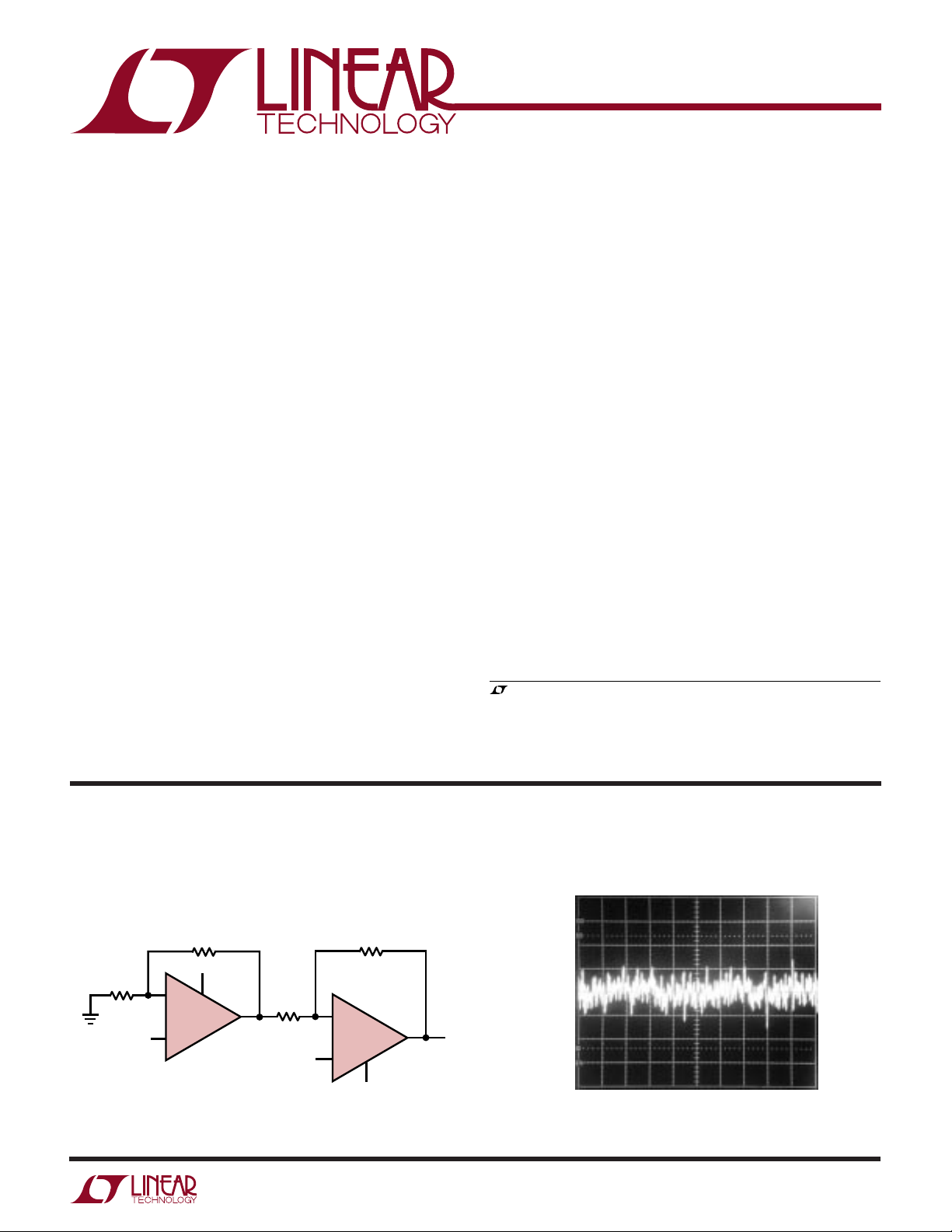
TYPICAL APPLICATIO
High Performance Low Cost Instrumentation Amplifier
R2
10k
0.1%
R1
100Ω
0.1%
5V
2
3
–V
IN
8
–
1/2
LTC2051HV
+
R1
100Ω
0.1%
1
V
IN
6
–
LTC2051HV
5
+
10k
0.1%
1/2
–5V
Input Referred Noise 0.1Hz to 10Hz
2
R2
1
0
µV
4
7
AV = 101
20512 TA01
–1
–2
0246810
TIME (SEC)
2052 TA02
1
LTC2051/LTC2052
1
2
3
4
OUT A
–IN A
+IN A
V
–
8
7
6
5
V
+
OUT B
–IN B
+IN B
TOP VIEW
MS8 PACKAGE
8-LEAD PLASTIC MSOP
TOP VIEW
V
+
OUT B
–IN B
+IN B
OUT A
–IN A
+IN A
V
–
1
2
3
4
8
7
6
5
S8 PACKAGE
8-LEAD PLASTIC SO
TOP VIEW
S PACKAGE
14-LEAD PLASTIC SO
1
2
3
4
5
6
7
14
13
12
11
10
9
8
OUT A
–IN A
+IN A
V
+
+IN B
–IN B
OUT B
OUT D
–IN D
+IN D
V
–
+IN C
–IN C
OUT C
WWWU
ABSOLUTE AXI U RATI GS
(Note 1)
Total Supply Voltage (V+ to V–)
LTC2051/LTC2052 .................................................. 7V
LTC2051HV/LTC2052HV ....................................... 12V
Input Voltage (Note 5) .......... (V+ + 0.3V) to (V– – 0.3V)
Output Short-Circuit Duration......................... Indefinite
UU
W
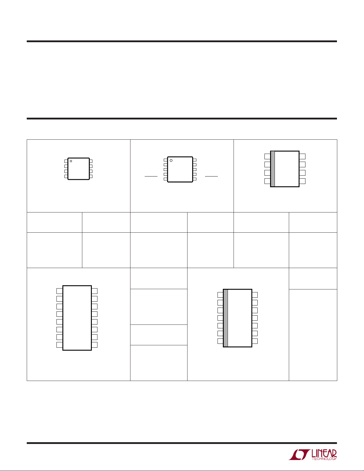
PACKAGE/ORDER I FOR ATIO
TOP VIEW
1
OUT A
2
–IN A
3
+IN A
–
4
V
SHDN A
5
MS10 PACKAGE
10-LEAD PLASTIC MSOP
T
= 125°C, θJA = 250°C/W
JMAX
ORDER PART
NUMBER
LTC2051CMS8
LTC2051IMS8
LTC2051HVCMS8
LTC2051HVIMS8
MS8 PART
MARKING
LTMN
LTMP
LTPJ
LTPK
LTC2051CMS10
LTC2051IMS10
LTC2051HVCMS10
LTC2051HVIMS10
T
= 125°C, θJA = 250°C/W
JMAX
ORDER PART
NUMBER
Operating Temperature Range ............... –40°C to 85°C
Specified Temperature Range (Note 3).. –40°C to 85°C
Storage Temperature Range ................ –65°C to 150°C
Lead Temperature (Soldering, 10 sec)................. 300°C
+
10
V
OUT B
9
–IN B
8
+IN B
7
SHDN B
6
T
= 125°C, θJA = 190°C/W
JMAX
MS10 PART
MARKING
LTMQ
LTMR
LTRB
LTRC
ORDER PART
NUMBER
LTC2051CS8
LTC2051IS8
LTC2051HVCS8
LTC2051HVIS8
S8 PART
MARKING
2051
2051I
2051HV
051HVI
TOP VIEW
1
OUT A
2
–IN A
3
+IN A
+
4
V
5
+IN B
6
–IN B
7
OUT B
8
NC
16-LEAD PLASTIC SSOP
T
= 125°C, θJA = 110°C/W
JMAX
GN PACKAGE
OUT D
16
–IN D
15
+IN D
14
V
13
+IN C
12
–IN C
11
OUT C
10
NC
9
Consult factory for Military grade parts.
2
ORDER PART
NUMBER
LTC2052CGN
LTC2052IGN
–
LTC2052HVCGN
LTC2052HVIGN
ORDER PART
NUMBER
LTC2052CS
LTC2052IS
LTC2052HVCS
LTC2052HVIS
GN PART
MARKING
2052
2052I
2052HV
T
= 125°C, θJA = 110°C/W
JMAX
052HVI
LTC2051/LTC2052
ELECTRICAL CHARACTERISTICS
(LTC2051/LTC2052, LTC2051HV/LTC2052HV) The ● denotes the
specifications which apply over the full operating temperature range, otherwise specifications are at TA = 25°C. VS = 3V, 5V
unless otherwise noted. (Note 3)
PARAMETER CONDITIONS MIN TYP MAX UNITS
Input Offset Voltage (Note 2) ±0.5 ±3 µV
Average Input Offset Drift (Note 2) ● 0.01 ±0.03 µV/°C
Long-Term Offset Drift 50 nV/√mo
Input Bias Current (Note 4) VS = 3V ±8 ±50 pA
= 3V ● ±100 pA
V
S
VS = 5V ±25 ±75 pA
= 5V ● ±150 pA
V
S
Input Offset Current (Note 4) VS = 3V ±100 pA
V
= 3V ● ±150 pA
S
VS = 5V ±150 pA
= 5V ● ±200 pA
V
S
Input Noise Voltage RS = 100Ω, DC to 10Hz 1.5 µV
Common Mode Rejection Ratio VCM = GND to V+ – 1.3, VS = 3V 115 130 dB
● 110 130 dB
VCM = GND to V+ – 1.3, VS = 5V 120 130 dB
● 115 130 dB
Power Supply Rejection Ratio 120 130 dB
● 115 130 dB
Large-Signal Voltage Gain RL = 10k, VS = 3V 120 140 dB
● 115 140 dB
RL = 10k, VS = 5V 125 140 dB
● 120 140 dB
Output Voltage Swing High RL = 2k to GND ● V+ – 0.15 V+ – 0.06 V
= 10k to GND ● V+ – 0.05 V+ – 0.02 V
R
L
Output Voltage Swing Low RL = 2k to GND ● 215mV
R
= 10k to GND ● 215mV
L
Slew Rate 2V/µs
Gain Bandwidth Product 3 MHz
Supply Current (Per Amplifier) No Load, VS = 3V, V
No Load, VS = 5V, V
Supply Current, Shutdown V
Shutdown Pin Input Low Voltage (VIL) ● V– + 0.5 V
Shutdown Pin Input High Voltage (V
Shutdown Pin Input Current V
Internal Sampling Frequency 7.5 kHz
) ● V+ – 0.5 V
IH
= VIL, VS = 3V ● 25µA
SHDN
= VIL, VS = 5V ● 410µA
V
SHDN
= VIL, VS = 3V ● –1 –3 µA
SHDN
= VIL, VS = 5V ● –2 –5 µA
V
SHDN
SHDN
SHDN
= V
= V
IH
IH
● 0.75 1.0 mA
● 0.85 1.2 mA
P-P
3
LTC2051/LTC2052
ELECTRICAL CHARACTERISTICS
(LTC2051HV/LTC2052HV) The ● denotes the specifications which apply over
the full operating temperature range, otherwise specifications are at TA = 25°C. VS = ±5V unless otherwise noted. (Note 3)
PARAMETER CONDITIONS MIN TYP MAX UNITS
Input Offset Voltage (Note 2) ±1 ±3 µV
Average Input Offset Drift (Note 2) ● 0.01 ±0.03 µV/°C
Long-Term Offset Drift 50 nV/√mo
Input Bias Current (Note 4) ±90 ±150 pA
● ±300 pA
Input Offset Current (Note 4) ±300 pA
● ±500 pA
Input Noise Voltage RS = 100Ω, DC to 10Hz 1.5 µV
Common Mode Rejection Ratio VCM = V– to V+ – 1.3 125 130 dB
● 120 130 dB
Power Supply Rejection Ratio 120 130 dB
● 115 130 dB
Large-Signal Voltage Gain RL = 10k 125 140 dB
● 120 140 dB
Maximum Output Voltage Swing RL = 2k to GND ● ±4.75 ±4.92 V
= 10k to GND ● ±4.90 ±4.98 V
R
L
Slew Rate 2V/µs
Gain Bandwidth Product 3 MHz
Supply Current (Per Amplifier) No Load, V
Supply Current, Shutdown V
Shutdown Pin Input Low Voltage (VIL) ● V– + 0.5 V
Shutdown Pin Input High Voltage (V
Shutdown Pin Input Current V
Internal Sampling Frequency 7.5 kHz
) ● V+ – 0.5 V
IH
SHDN
SHDN
= V
= V
SHDN
IL
IL
= V
IH
● 1 1.5 mA
● 15 30 µA
● –7 –15 µA
P-P
Note 1: Absolute Maximum Ratings are those values beyond which the life
of the device may be impaired.
Note 2: These parameters are guaranteed by design. Thermocouple effects
preclude measurements of these voltage levels during automated testing.
Note 3: The LTC2051C/LTC2052C, LTC2051HVC/LTC2052HVC are
guaranteed to meet specified performance from 0°C to 70°C and are
designed, characterized and expected to meet these extended temperature
limits, but are not tested at –40°C and 85°C. The LTC2051I/LTC2052I,
LTC2051HVI/LTC2052HVI are guaranteed to meet the extended
temperature limits.
Note 4: The bias current measurement accuracy depends on the proximity
of the negative supply bypass capacitors to the device under test. Because
of this, only the bias current of channel B (LTC2051) and channels A and B
(LTC2052) are 100% tested to the data sheet specifications. The bias
currents of the remaining channels are 100% tested to relaxed limits,
however, their values are guaranteed by design to meet the data sheet
limits.
Note 5: This parameter is guaranteed to meet specified performance
through design and characterization. It has not been tested.
4

UW
TYPICAL PERFOR A CE CHARACTERISTICS
LTC2051/LTC2052
Common Mode Rejection Ratio
vs Frequency
140
120
100
80
60
CMRR (dB)
40
20
0
10 10k
1 100 1k 100k
FREQUENCY (Hz)
VS = 3V OR ±5V
= 0.5V
V
CM
Output Voltage Swing
vs Load Resistance
6
RL TO GND
5
4
3
2
OUTPUT SWING (V)
1
0
0
246
LOAD RESISTANCE (kΩ)
= 5V
V
S
= 3V
V
S
DC CMRR
vs Common Mode Input Range PSRR vs Frequency
120
100
–PSRR
80
60
PSRR (dB)
40
20
0
10 1k 10k 1M
+PSRR
100
FREQUENCY (Hz)
100k
20512 G03
P-P
20512 G01
140
120
100
80
60
CMRR (dB)
40
20
0
0
VS = 10V
VS = 3V
24 10
VS = 5V
68
VCM (V)
20512 G02
Output Swing
Output Swing vs Output Current
6
5
4
3
2
OUTPUT VOLTAGE (V)
1
0
10
8
20512 G04
0.01
VS = 5V
VS = 3V
0.1 1 10
OUTPUT CURRENT (mA)
20512 G05
vs Load Resistance ±5V
5
4
RL TO GND
3
2
1
0
–1
–2
OUTPUT VOLTAGE (V)
–3
–4
–5
2
0
LOAD RESISTANCE (kΩ)
6
8
4
10
20512 G06
Output Swing
vs Output Current, ±5V Supply
5
4
RL TO GND
3
2
1
0
–1
OUTPUT SWING (V)
–2
–3
–4
–5
0.01
0.1
OUTPUT CURRENT (mA)
Gain/Phase vs Frequency
20512 G08
80
100
120
140
160
180
200
PHASE (DEG)
100
80
60
40
20
GAIN (dB)
0
VS = 3V OR ±5V
–20
= 50pF
C
L
= 100k
R
L
1
20512 G07
–40
10
1k 1M
100 10k 100k 10M
FREQUENCY (Hz)
PHASE
GAIN
Bias Current vs Temperature
10k
1k
100
BIAS CURRENT (pA)
10
1
–50 50 100 125
VS = ±5V
VS = 5V
VS = 3V
0
TEMPERATURE (°C)
20512 G09
5

LTC2051/LTC2052
UW
TYPICAL PERFOR A CE CHARACTERISTICS
Input Bias Current
vs Input Common Mode Voltage
250
200
Transient Response
Input Overload Recovery
0
–0.1
INPUT (V)
150
100
INPUT BIAS CURRENT (pA)
50
0
–3
–5
–1 0
INPUT COMMON MODE VOLTAGE (V)
SAMPLING FREQUENCY (kHz)
VS = ±5V
V
= 5V
S
V
= 3V
S
1
3
20512 G10
Sampling Frequency
vs Supply Voltage
10
9
8
7
6
5
3
5
SUPPLY VOLTAGE (V)
2V/DIV
AV = 1
= 10k
R
L
C
= 100pF
L
= ±5V
V
5
S
1µs/DIV
20512 G11
1.5
OUTPUT (V)
0
AV = –100
R
L
C
L
V
S
= 100k
= 10pF
= 3V
500µs/DIV
2050 G12
Sampling Frequency
vs Temperature
10
9
8
7
SAMPLING FREQUENCY (kHz)
6
7
9
11
20512 G13
5
–50
VS = ±5V
V
= 3V
S
0
TEMPERATURE (°C)
50
100
20512 G14
125
6
Supply Current (Per Amplifier)
vs Supply Voltage
1.2
1.0
0.8
0.6
0.4
SUPPLY CURRENT (mA)
0.2
0
2.5
4.5 6.5 8.5 10.5
SUPPLY VOLTAGE (V)
20512 G15
Supply Current (Per Amplifier)
vs Temperature
1.2
1.0
0.8
0.6
0.4
SUPPLY CURRENT (mA)
0.2
0
–50
0
TEMPERATURE (°C)
50
VS = ±5V
VS = 5V
VS = 3V
100
20512 G16
125

WUUU
APPLICATIO S I FOR ATIO
LTC2051/LTC2052
Shutdown
The LTC2051 includes a shutdown pin in the 10-lead
MSOP. When this active low pin is high or allowed to float,
the device operates normally. When the shutdown pin is
pulled low, the device enters shutdown mode; supply
current drops to 3µA, all clocking stops and the output
assumes a high impedance state.
Clock Feedthrough, Input Bias Current
The LTC2051/LTC2052 use autozeroing circuitry to achieve
an almost zero DC offset over temperature, common
mode voltage and power supply voltage. The frequency of
the clock used for autozeroing is typically 7.5kHz. The
term clock feedthrough is broadly used to indicate visibility of this clock frequency in the op amp output spectrum.
There are typically two types of clock feedthrough in
autozeroed op amps like the LTC2051/LTC2052.
The first form of clock feedthough is caused by the settling
of the internal sampling capacitor and is input referred;
that is, it is multiplied by the closed-loop gain of the op
amp. This form of clock feedthrough is independent of the
magnitude of the input source resistance or the magnitude
of the gain setting resistors. The LTC2051/LTC2052 have
a residue clock feedthrough of less than 1µV
referred at 7.5kHz.
RMS
input
To reduce this form of clock feedthrough, use smaller
valued gain setting resistors and minimize the source
resistance at the input. If the resistance seen at the inputs
is less than 10k, this form of clock feedthrough is less
than 1µV
amount of residue clock feedthrough from the first form
previously described.
Placing a capacitor across the feedback resistor reduces
either form of clock feedthrough by limiting the bandwidth
of the closed-loop gain.
Input bias current is defined as the DC current into the
input pins of the op amp. The same current spikes that
cause the second form of clock feedthrough
described
current of the op amp below 70°C.
At temperatures above 70°C, the leakage of the ESD
protection diodes on the inputs increase the input bias
currents of both inputs in the positive direction, while the
current caused by the charge injection stays relatively
constant. At elevated temperatures (above 85°C) the
leakage current begins to dominate and both the negative
and positive pin’s input bias currents are in the positive
direction (into the pins).
Input Pins, ESD Sensitivity
input referred at 7.5kHz, or less than the
RMS
previously
, when averaged, dominate the DC input bias
The second form of clock feedthrough is caused by the
small amount of charge injection occurring during the
sampling and holding of the op amps input offset voltage.
The current spikes are multiplied by the impedance seen
at the input terminals of the op amp, appearing at the
output multiplied by the closed-loop gain of the op amp.
ESD voltages above 700V on the input pins of the op amp
will cause the input bias currents to increase (more DC
current into the pins). At these voltages, it is possible to
damage the device to a point where the input bias current
exceeds the maximums specified in this data sheet.
7

LTC2051/LTC2052
TYPICAL APPLICATIO
U
The dual chopper op amp buffers the inputs of A1 and
corrects its offset voltage and offset voltage drift. With the
RC values shown, the power-up warm-up time is typically
20 seconds. The step response of the composite amplifier
does not present settling tails. The LT®1677 should be
used when extremely low noise, VOS and VOS drift are
Obtaining Ultralow VOS Drift and Low Noise
+
5
2
–
1/2 LTC2051
3
+
R1
3
+
–
2
–
R4
1
5V
R2
1
8
A1
+
1/2 LTC2051
6
–
R5
R3
6
OUT
needed and the input source resistance is low. (For instance a 350Ω strain gauge bridge.) The LT1012 or
equivalent should be used when low bias current (100pA)
is also required in conjunction with DC to 10Hz low noise,
low VOS and VOS drift. The measured typical input offset
voltages are less than 1µV.
7
C1
OUT
C2
20512 F01
A1 R1 R2 R3 R4 R5 C1 C2 eIN (DC – 1Hz) eIN (DC – 10Hz)
LT1677 2.49k 3.01k 340k 10k 100k 0.01µF 0.001µF 0.15µV
LT1012 750Ω 57Ω 250k 10k 100k 0.01µF 0.001µF 0.3µV
P-P
P-P
8
0.2µV
0.4µV
P-P
P-P

PACKAGE DESCRIPTIO
LTC2051/LTC2052
U
Dimensions in inches (millimeters) unless otherwise noted.
MS8 Package
8-Lead Plastic MSOP
(LTC DWG # 05-08-1660)
0.118 ± 0.004*
(3.00 ± 0.102)
8
7
6
5
0.193 ± 0.006
(4.90 ± 0.15)
12
0.040
± 0.006
SEATING
PLANE
(1.02 ± 0.15)
0.012
(0.30)
0.0256
REF
(0.65)
BSC
0.007
(0.18)
0.021
± 0.006
(0.53 ± 0.015)
* DIMENSION DOES NOT INCLUDE MOLD FLASH, PROTRUSIONS OR GATE BURRS. MOLD FLASH,
PROTRUSIONS OR GATE BURRS SHALL NOT EXCEED 0.006" (0.152mm) PER SIDE
** DIMENSION DOES NOT INCLUDE INTERLEAD FLASH OR PROTRUSIONS.
INTERLEAD FLASH OR PROTRUSIONS SHALL NOT EXCEED 0.006" (0.152mm) PER SIDE
° – 6° TYP
0
0.118 ± 0.004**
4
3
0.034 ± 0.004
(0.86 ± 0.102)
(3.00 ± 0.102)
0.006 ± 0.004
(0.15 ± 0.102)
MS10 Package
10-Lead Plastic MSOP
(LTC DWG # 05-08-1661)
0.118 ± 0.004*
(3.00 ± 0.102)
8910
7
6
MSOP (MS8) 1098
3
45
0.118 ± 0.004**
(3.00 ± 0.102)
0.034 ± 0.004
(0.86 ± 0.102)
0.006 ± 0.004
(0.15 ± 0.102)
0.193 ± 0.006
(4.90 ± 0.15)
12
0.040
± 0.006
SEATING
PLANE
(1.02 ± 0.15)
0.009
(0.228)
0.0197
REF
(0.50)
BSC
0.007
(0.18)
0.021
± 0.006
(0.53 ± 0.015)
* DIMENSION DOES NOT INCLUDE MOLD FLASH, PROTRUSIONS OR GATE BURRS. MOLD FLASH,
PROTRUSIONS OR GATE BURRS SHALL NOT EXCEED 0.006" (0.152mm) PER SIDE
** DIMENSION DOES NOT INCLUDE INTERLEAD FLASH OR PROTRUSIONS.
INTERLEAD FLASH OR PROTRUSIONS SHALL NOT EXCEED 0.006" (0.152mm) PER SIDE
° – 6° TYP
0
MSOP (MS10) 1098
9

LTC2051/LTC2052
PACKAGE DESCRIPTIO
U
Dimensions in inches (millimeters) unless otherwise noted.
S8 Package
8-Lead Plastic Small Outline (Narrow 0.150)
(LTC DWG # 05-08-1610)
0.189 – 0.197*
(4.801 – 5.004)
7
8
5
6
0.228 – 0.244
(5.791 – 6.197)
0.010 – 0.020
(0.254 – 0.508)
0.008 – 0.010
(0.203 – 0.254)
*
DIMENSION DOES NOT INCLUDE MOLD FLASH. MOLD FLASH
SHALL NOT EXCEED 0.006" (0.152mm) PER SIDE
**
DIMENSION DOES NOT INCLUDE INTERLEAD FLASH. INTERLEAD
FLASH SHALL NOT EXCEED 0.010" (0.254mm) PER SIDE
× 45°
0°– 8° TYP
0.016 – 0.050
(0.406 – 1.270)
GN Package
16-Lead Plastic SSOP (Narrow 0.150)
(LTC DWG # 05-08-1641)
0.053 – 0.069
(1.346 – 1.752)
0.014 – 0.019
(0.355 – 0.483)
TYP
0.150 – 0.157**
(3.810 – 3.988)
1
2
16
15
3
4
0.189 – 0.196*
(4.801 – 4.978)
12 11 10
14
13
0.004 – 0.010
(0.101 – 0.254)
0.050
(1.270)
BSC
9
SO8 1298
0.009
(0.229)
REF
10
0.015
± 0.004
(0.38 ± 0.10)
0.007 – 0.0098
(0.178 – 0.249)
0.016 – 0.050
(0.406 – 1.270)
* DIMENSION DOES NOT INCLUDE MOLD FLASH. MOLD FLASH
SHALL NOT EXCEED 0.006" (0.152mm) PER SIDE
** DIMENSION DOES NOT INCLUDE INTERLEAD FLASH. INTERLEAD
FLASH SHALL NOT EXCEED 0.010" (0.254mm) PER SIDE
0° – 8° TYP
× 45°
0.229 – 0.244
(5.817 – 6.198)
0.053 – 0.068
(1.351 – 1.727)
0.008 – 0.012
(0.203 – 0.305)
12
0.150 – 0.157**
(3.810 – 3.988)
5
4
678
3
0.004 – 0.0098
(0.102 – 0.249)
0.0250
(0.635)
BSC
GN16 (SSOP) 1098

PACKAGE DESCRIPTIO
LTC2051/LTC2052
U
Dimensions in inches (millimeters) unless otherwise noted.
S Package
14-Lead Plastic Small Outline (Narrow 0.150)
(LTC DWG # 05-08-1610)
0.337 – 0.344*
(8.560 – 8.738)
13
12
11
10
14
9
8
0.228 – 0.244
(5.791 – 6.197)
0.010 – 0.020
(0.254 – 0.508)
0.008 – 0.010
(0.203 – 0.254)
*
DIMENSION DOES NOT INCLUDE MOLD FLASH. MOLD FLASH
SHALL NOT EXCEED 0.006" (0.152mm) PER SIDE
**
DIMENSION DOES NOT INCLUDE INTERLEAD FLASH. INTERLEAD
FLASH SHALL NOT EXCEED 0.010" (0.254mm) PER SIDE
× 45°
0.016 – 0.050
(0.406 – 1.270)
0.053 – 0.069
(1.346 – 1.752)
0° – 8° TYP
0.014 – 0.019
(0.355 – 0.483)
TYP
0.150 – 0.157**
(3.810 – 3.988)
1
3
2
4
5
0.050
(1.270)
BSC
6
7
0.004 – 0.010
(0.101 – 0.254)
S14 1298
Information furnished by Linear Technology Corporation is believed to be accurate and reliable.
However, no responsibility is assumed for its use. Linear Technology Corporation makes no representation that the interconnection of its circuits as described herein will not infringe on existing patent rights.
11

LTC2051/LTC2052
TYPICAL APPLICATIO
U
Paralleling Amplifiers to Improve Noise
R2
R1
2
–
1/4 LTC2052
3
+
R
1
R
R2
R1
V
IN
V
OUT
V
IN
6
–
1/4 LTC2052
5
+
R2
R1
9
–
1/4 LTC2052
10
+
R2
= 3 ; INPUT DC – 10Hz NOISE ≅ 0.8µV
R1
R
7
R
8
P-P
=
5V
0.1µF
13
12
NOISE OF EACH PARALLEL OP AMP
4
–
1/4 LTC2052
+
11
–5V
14
0.1µF
√3
20512 F02
V
OUT
RELATED PARTS
PART NUMBER DESCRIPTION COMMENTS
LTC1051/LTC1053 Precision Zero-Drift Op Amp Dual/Quad
LTC1151 ±15V Zero-Drift Op Amp Dual High Voltage Operation ±18V
LTC1152 Rail-to-Rail Input and Output Zero-Drift Op Amp Single Zero-Drift Op Amp with Rail-to-Rail Input and Output and Shutdown
LTC2050 Zero-Drift Op Amp in SOT-23 Single Supply Operation 2.7V to ±5V, Shutdown
20512f LT/TP 1100 4K • PRINTED IN USA
LINEAR TECHNOLOGY CORPORATION 2000
12
Linear Technology Corporation
1630 McCarthy Blvd., Milpitas, CA 95035-7417
(408) 432-1900 ● FAX: (408) 434-0507
●
www.linear-tech.com
 Loading...