

Linear Technology LTC2050 Datasheet

LTC2050
Final Electrical Specifications
Zero-Drift
Operational Amplifier
in SOT-23
November 1999
EATU
F
■
SOT-23 Package
■
Maximum Offset Voltage of 3µV
■
Maximum Offset Voltage Drift of 30nV/°C
■
Noise: 1.5µV
■
Voltage Gain: 140dB (Typ)
■
PSRR: 130dB (Typ)
■
CMRR: 130dB (Typ)
■
Supply Current: 0.8mA (Typ)
■
Single Supply Operation: 2.7V to 6V
■
Extended Common Mode Input Range
■
Output Swings Rail-to-Rail
■
Overload Recovery Time: 2ms (Typ)
PPLICATI
A
■
Thermocouple Amplifiers
■
Electronic Scales
■
Medical Instrumentation
■
Strain Gauge Amplifiers
■
High Resolution Data Acquisition
■
DC Accurate RC Active Filters
RE
S
(0.1Hz to 10Hz Typ)
P-P
U
O
S
DUESCRIPTIO
The LTC®2050 is a low drift operational amplifier available
in the 5- or 6-lead SOT-23 and SO-8 packages. It operates
from a single 2.7V supply while still supporting 5V applications. The power consumption is 800µA and the ver-
sions in the 6-lead SOT-23 and SO-8 packages offer power
shutdown (active low).
The LTC2050, despite its miniature size, features uncompromising DC performance. The typical input offset voltage and offset drift are 0.5µV and 10nV/°C. The almost
zero DC offset and drift are supported with a power supply
rejection ratio (PSRR) and common mode rejection ratio
(CMRR) of more than 130dB.
The input common mode voltage ranges from the negative
supply up to 1V from the positive supply. The LTC2050
also has an enhanced output stage capable of driving
loads as low as 1kΩ to both supply rails. The open-loop
gain, loaded with 1kΩ, is in excess of 140dB. The LTC2050
also features a 1.5µV
bandwidth product.
, LTC and LT are registered trademarks of Linear Technology Corporation.
DC to 10Hz noise and a 3MHz gain
P-P
A
PPLICATITYPICAL
5V
50Ω
GAIN
TRIM
350Ω
STRAIN
GAUGE
U
O
Differential Bridge Amplifier
5V
0.1µF
2
–
3
+
1000pF
18.2k
Information furnished by Linear Technology Corporation is believed to be accurate and reliable.
However, no responsibility is assumed for its use. Linear Technology Corporation makes no representation that the interconnection of its circuits as described herein will not infringe on existing patent rights.
1000pF
18.2k
7
LTC2050
4
2050 TA01
Input Referred Noise 0.1Hz to 10Hz
VS = 5V
3
1
0
µV
6
A
= 100
V
–1
–3
2
0
4
TIME (s)
6
8
10
LT2050 TA02
1
LTC2050
A
W
O
LUTEXI TIS
S
A
WUW
U
ARB
G
(Note 1)
Total Supply Voltage (V+ to V–) ............................... 7V
Input Voltage ........................ (V+ + 0.3V) to (V– – 0.3V)
Output Short-Circuit Duration......................... Indefinite
Operating Temperature Range ............... –40°C to 85°C
WU
/
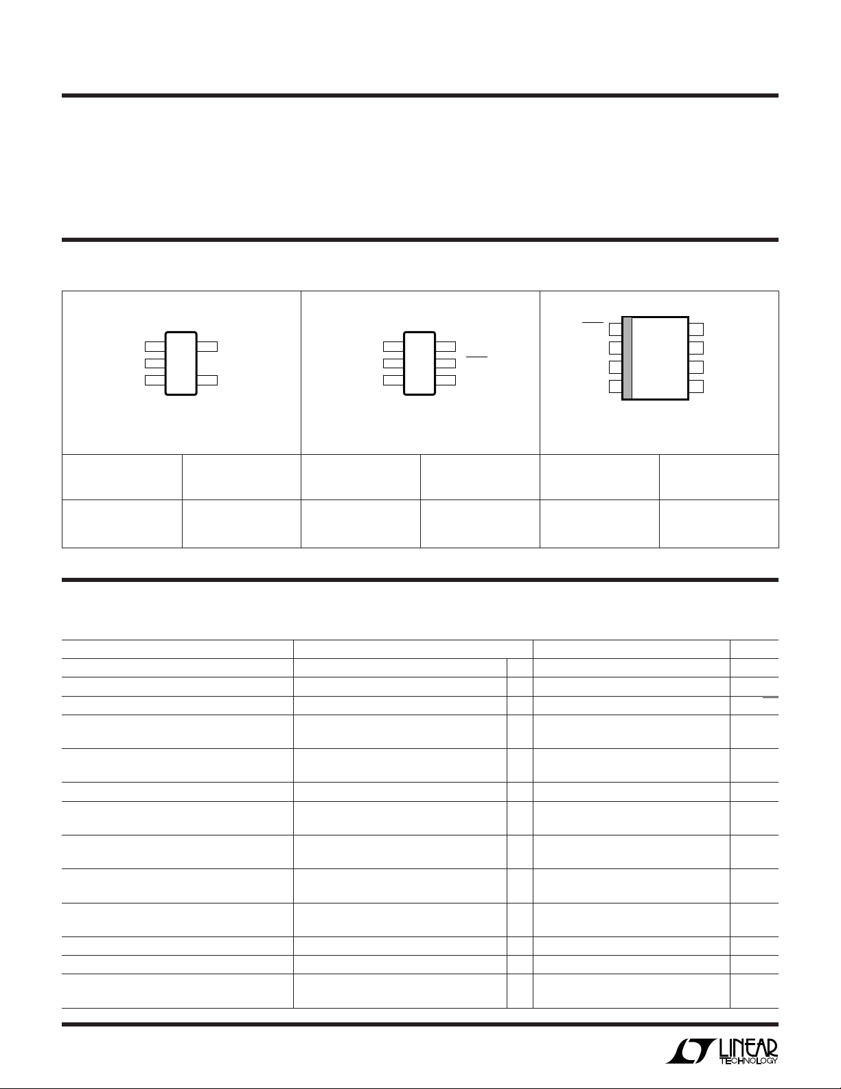
PACKAGE
OUT 1
V
+IN 3
ORDER PART
NUMBER
O
RDER I FOR ATIO
TOP VIEW
–
2
S5 PACKAGE
5-LEAD PLASTIC SOT-23
= 125°C, θJA = 250°CW
JMAX
MARKING
+
5 V
4 –IN
S5 PART
OUT 1
–
2
V
+IN 3
S6 PACKAGE
6-LEAD PLASTIC SOT-23
T
= 125°C, θJA = 230°CWT
JMAX
ORDER PART
NUMBER
Specified Temperature Range (Note 3).. –40°C to 85°C
Storage Temperature Range ................ –65°C to 150°C
Lead Temperature (Soldering, 10 sec)................. 300°C
U
TOP VIEW
TOP VIEW
+
6 V
5 SHDN
4 –IN
S6 PART
MARKING
SHDN
1
–IN
2
+IN
3
–
V
4
S8 PACKAGE
8-LEAD PLASTIC SO
T
= 125°C, θJA = 190°CW
JMAX
ORDER PART
NUMBER
8
7
6
5
S8 PART
MARKING
NC
V
OUT
NC
+
LTC2050CS5
LTIN
LTC2050CS6
LTIP
LTC2050CS8
LTC2050IS8
Consult factory for Military grade parts.
LECTRICAL C CHARA TERIST
E
temperature range, otherwise specifications are at TA = 25°C. VS = 3V unless otherwise noted. (Note 3)
PARAMETER CONDITIONS MIN TYP MAX UNITS
Input Offset Voltage (Note 2) ±0.5 ±3 µV
Average Input Offset Drift (Note 2) ● ±0.03 µV/°C
Long-Term Offset Drift 50 nV/√mo
Input Bias Current ±20 ±75 pA
Input Offset Current ±150 pA
Input Noise Voltage RS = 100Ω, DC to 10Hz 1.5 µV
Common Mode Rejection Ratio VCM = V– to V+ – 1.3 115 130 dB
Power Supply Rejection Ratio 120 130 dB
Large-Signal Voltage Gain RL = 10k 120 140 dB
Maximum Output Voltage Swing RL = 2k ● 2.85 2.94 V
Slew Rate 2V/µs
Gain Bandwidth Product 3 MHz
Supply Current V
ICS
R
= 10k ● 2.95 2.98 V
L
= V+, No Load ● 0.75 1.1 mA
SHDN
V
= V
SHDN
The ● denotes the specifications which apply over the full operating
● ±300 pA
● ±200 pA
● 110 130 dB
● 115 130 dB
● 115 140 dB
–
● 10 µA
2050
2050I
P-P
2
 Loading...