

advertisement
Easy-to-Use Differential Amplifiers Simplify Balanced
Signal Designs – Design Note 333
Jon Munson
Introduction
The LTC®1992 product family provides simple amplification or level translation solutions for amplifying signals
that are intrinsically differential or need to be made
differential. In addition to the uncommitted configuration
of the base LTC1992, fixed gain versions with spacesaving on-chip factory-trimmed resistors are available as
the LTC1992-1, LTC1992-2, LTC1992-5 and LTC1992-10,
where the nominal gain is indicated by the suffix dash
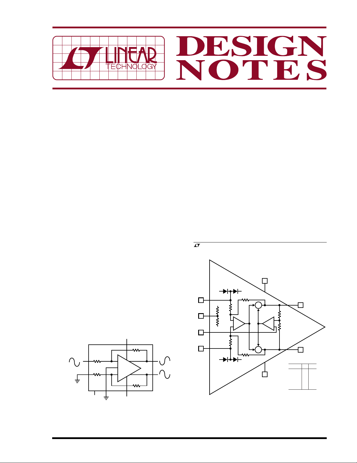
number. Figure 1 shows a typical gain-of-ten application
where all gain setting components are included in the tiny
8-lead MSOP package.
Easy-to-Use Circuit Topology
The block diagram in Figure 2 shows the general configuration of the differential-in/differential-out CMOS amplifier core, along with an output common mode servo. The
values of the on-chip gain resistors depend on the dash
suffix of the device as indicated. A convenient on-chip
voltage-divider resistor network is also provided to support applications where a source of mid-supply potential
(V
) is needed.
MID
The LTC1992 is easy to use. Any signal difference at the
inputs (within the input common mode range) are amplified and presented as a voltage difference at the output
5V
3
+V
LTC1992-10
+1V
V
IN
–1V
15k
1
V
OCM
8
15k
V
MID
7
S
150k
–
+
–
+
150k
–V
S
2
–5V
DN333 F01
6
+5V
4
–5V
+5V
5
–5V
pins with a gain bandwidth product of about 4MHz. The
differential gain, A, is set by resistor values:
A = R
F/RG
Any input common mode induced errors, primarily caused
by small mismatches of resistor values, appear at the
output as differential error. The common mode (shared
offset) of the output pair is (V
OUT
+
+ V
pendently governed to track the user-supplied V
put common mode control voltage (V
strapped to V
if desired). The uncommitted LTC1992
MID
–
)/2 and inde-
OUT
may be simply
OCM
OCM
out-
(no dash suffix) may be user configured for any desired
differential gain by selection of external resistors, or
configured specifically for other specialized uses.
, LTC and LT are registered trademarks of Linear Technology Corporation.
+V
S
3
–V
S
1
–IN
V
MID
V
OCM
+IN
+V
S
–V
–V
S
DN333 F02
200k
200k
S
7
2
8
+V
S
R
F
+
R
G
–
+
R
G
Σ
+
30k
–
A2
+
30k
+
Σ
R
F
–
+V
S
6
–V
S
SUFFIX
-10
-5
-2
-1
NONE
+OUT
4
–OUT
5
R
R
G
F
15k
150k
30k
150k
30k
60k
30k
30k
0
∞
Figure 1. Typical Single-Ended to Differential Conversion Figure 2. LTC1992 Functional Block Diagram
03/04/333
Common Mode Range Considerations
For a given input common mode voltage (V
output common mode voltage (V
), the designer must
OCM
INCM
) and
verify that voltage appearing at the internal amplifier
inputs (V
–V
– 0.1V to +VS – 1.3V. With a standard differential
S
) is within the specified operating range of
ICM
amplifier topology having a closed loop gain of A, the
following relationship holds:
= (A/(A+1)) • V
V
ICM
+ (1/(A+1)) • V
INCM
OCM
For example, assume an LTC1992 (no dash) is powered
from 5V, configured for a gain of 2.5 with V
V
(i.e. 2.5V), and driven from a source with common
MID
mode of 0V. From the relation above, V
ICM
tied to
OCM
is (2.5/3.5) •
0 + (1/3.5) • 2.5 = 0.71V, which is well within the
performance range of the device. In this example, the
outputs can swing ±2.5V around the 2.5V V
OCM
level.
Therefore, the differential inputs can swing 1V below
ground without clipping effects or the need for a minus
rail. The dash suffix versions have an additional input
limitation due to the possibility of forward biasing the
ESD input protection diodes (shown in the Figure 2),
which limit the maximum allowable signal swings to 0.3V
beyond the supply voltages (while the base LTC1992 also
includes the ESD diodes, conduction can only occur
outside the usable V
ICM
range).
Common Mode Input Range Extension
Use of the non-committed LTC1992 provides the possibility of extending input common mode capability well
outside the supply range by operating with a gain below
+
LTC1992
–
m =
m • V
A + m
R
F
–
V
+
R
F
RG + R
OCM
OUT
DN333 F03
R
S
S
= 2.5V
OCM
< 38V
INCM
R
G
R
S
V
V
IN
GAIN: A =
COMMON MODE SCALING:
V
ICM
EXAMPLE: ASSUME A = 1, m = 0.1, 5V SUPPLY, V
THUS: R
FOR 0.1% RESISTORS, CMRR ≥ 48dB
OCM
V
MID
R
S
R
G
R
F
R
G
A • m • V
INCM
=+
A + m
= RG = 30.1k, RS = 3.32k, –3.6V < V
F
Figure 3. Extending Input Common Mode Range
unity and/or introducing common mode shunt resistors
(see R
method is that component tolerances of R
in Figure 3). The drawback to the shunt resistor
S
and R
G
S
become magnified by the common mode improvement of
the circuit (approximately), leading to reduced CMRR
performance for a given resistor tolerance. For low gain
operation, common mode extension of 10× is realizable
with the use of high accuracy resistor networks.
Versatile Functional Block
The LTC1992 family is especially useful for making conversions to or from differential signaling. Analog-todigital converters (ADCs) are often optimized for differential
inputs with a specific common mode input voltage. Use of
an LTC1992 amplifier simplifies the ADC interface by
using the V
control feature to establish the requisite
OCM
offset. In many cases, the mid-scale potential is provided
by the ADC and can be tied directly to the V
OCM
input. In
addition, the source signal input may then be differential
or single ended (by grounding the unused input) or have
inverted polarity.
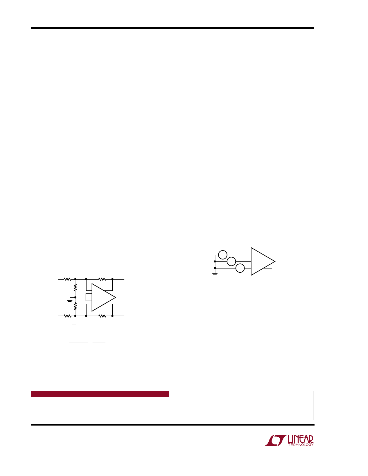
Since it is not necessary to connect to both outputs, one
can treat the part as single ended which provides the
useful feature that the V
input represents a third
OCM
algebraic input term (see Figure 4). This capability is
useful in performing analog addition or simple translation
functions.
V
INA
V
INB
V1 = V
+ V
INA
V2 = –V
+ V
INA
Figure 4. Single Ended Adder/Subtractor
+
V
OCM
LTC1992-2
V
–
INC
– V
INB
INC
+ V
INB
INC
–
+
DN333 F04
V2
V1
Conclusion
The LTC1992 family of differential amplifiers offers easyto-use building blocks that provide simple, minimum
component-count solutions to balanced-signal designs.
These parts are useful in a wide range of applications,
including simple methods of transforming signals to/from
differential form to providing component-free gain or DC
offset functions.
Data Sheet Download
http://www.linear.com/go/dnLTC1992
Linear Technology Corporation
1630 McCarthy Blvd., Milpitas, CA 95035-7417
(408) 432-1900 ● FAX: (408) 434-0507 ● www.linear.com
For applications help,
call (408) 432-1900, Ext. 2156
dn333f LT/TP 0304 305K • PRINTED IN THE USA
LINEAR TECHNOLOGY CORPORATION 2004
 Loading...