

Linear Technology LTC1986 Datasheet
FEATURES
■
VIN Range: 2.6V to 4.4V
■
Step-Up Charge Pump Generates 5V
■
Output Current: 10mA
■
VIN to V
■
Ultralow Power
Direct Connection for 3V SIMs
OUT
Operating Current: 14µA
Shutdown Current: <1µA
■
No Inductors
■
Short-Circuit/Thermal Protected
■
Switching Frequency: 900kHz
■
Soft-Start Limits Inrush Current at Turn-On
■
Output Driven to Ground During Shutdown
■
Ultrasmall Application Circuit (<0.045in2)
■
6-Lead SOT-23 Package
U
APPLICATIO S
■
GSM Cellular Telephones
■
PCS/DCS Cellular Telephones
■
Portable POS Terminals
LTC1986
3V/5V SIM Power Supply
in SOT-23
U
DESCRIPTIO
The LTC®1986 is a micropower charge pump DC/DC
converter that provides power for either 3V or 5V GSM
SIM cards. It operates in one of three modes: V
(5V mode), V
= VIN (3V mode) or shutdown. The input
OUT
voltage range is 2.6V to 4.4V and the part can provide
10mA of output current. The LTC1986 allows VIN to drop
as low as 2.6V by providing a boost feature in 3V mode. In
3V mode, V
is connected directly to VIN through a 2.5Ω
OUT
switch until VIN drops below 2.85V. When VIN is below
2.85V, the part automatically boosts V
regulated 2.9V output, thereby ensuring V
to maintain a
OUT
stays within
OUT
the 3V SIM VCC specification.
Extremely low operating current (14µA typical with no
load) and low external parts count make the part ideally
suited for small, light load battery-powered applications.
The total PCB area of the application circuit shown below
is less than 0.045in2. Protection features include inrush
current limiting, undervoltage lockout, short circuit and
thermal overload protection. The LTC1986 is available in
a 6-lead SOT-23 package.
, LTC and LT are registered trademarks of Linear Technology Corporation.
OUT
= 5V
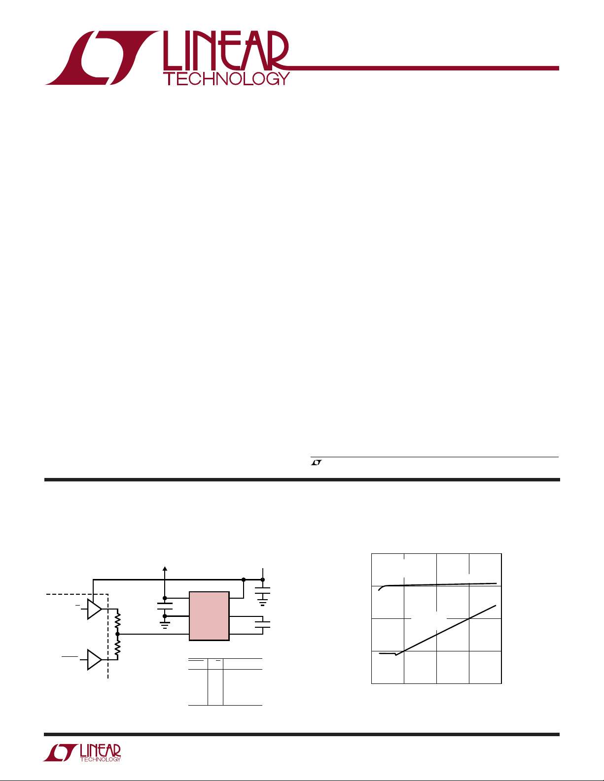
TYPICAL APPLICATIO
3V/5V SIM Power Supply
V
= 5V
OUT
OR V
IN
GSM
CONTROLLER
3/5
SHDN
2.2µF
1M
750k
1
2
3
V
GND
MODE
SHDN
0
0
1
1
U
LTC1986
OUT
3/5
V
IN
+
C1
–
C1
0
SHUTDOWN
1
SHUTDOWN
0
1
V
= 2.6V TO 4.4V
IN
6
5
4
MODE
= 5V
V
OUT
= V
V
OUT
Output Voltage vs Input Voltage
6
TA = 25°C
I
= 10mA
OUT
0.1µF
0.047µF
IN
1986 TA01
5
4
OUTPUT VOLTAGE (V)
3
2
2.5
3.0
3V MODE
(V
OUT
INPUT VOLTAGE (V)
= VIN)
3.5
5V MODE
4.0
4.5
1986 TA02
1
LTC1986
WW
W
ABSOLUTE MAXIMUM RATINGS
U
U
W
PACKAGE/ORDER INFORMATION
U
(Note 1)
VIN, V
to GND .........................................–0.3V to 6V
OUT
All Other Pins to GND ..................................–0.3V to 6V
V
Short-Circuit Duration............................. Indefinite
OUT
Operating Temperature Range
(Note 2) .................................................. – 40°C to 85°C
Storage Temperature Range ................. –65°C to 150°C
Lead Temperature (Soldering, 10 sec).................. 300°C
TOP VIEW
V
1
OUT
GND 2
MODE 3
S6 PACKAGE
6-LEAD PLASTIC SOT-23
T
= 125°C, θJA = 230°C/ W
JMAX
Consult factory for Military grade parts.
6 V
5 C1
4 C1
IN
+
–
ORDER PART
NUMBER
LTC1986ES6
S6 PART MARKING
LTKX
ELECTRICAL CHARACTERISTICS
The ● denotes specifications which apply over the full operating temperature range, otherwise specifications are TA = 25°C.
VIN = V
PARAMETER CONDITIONS MIN TYP MAX UNITS
V
IN
VOUT
V
IN
VIN-to-V
V
OUT
V
OUT
Switching Frequency Oscillator Free-Running 900 kHz
MODE Input Ranges Shutdown Mode
MODE Input Current ● –1 1 µA
Undervoltage Lockout Threshold 1.4 V
Note 1: Absolute Maximum Ratings are those values beyond which the life
of a device may be impaired.
to V
MIN
Operating Voltage ● 2.6 4.4 V
Output Voltage Shutdown Mode 0 V
Operating Current Shutdown Mode, V
ON Resistance 3V Mode, VIN = 3V ● 2.5 5 Ω
OUT
Short-Circuit Current 3V or 5V Mode, V
Discharge Resistance ● 70 200 Ω
, MODE = VIN, C1 = 0.047µF, C
MAX
= 2.2µF, unless otherwise specified.
OUT
3V Mode. V
3V Mode, V
5V Mode, V
5V Mode, VIN = 2.7V to 4.4V, I
3V Mode, I
5V Mode, I
5V Mode
3V Mode ● V
= 2.85V to 4.4V, I
IN
< 2.85V, I
IN
< 2.7V, I
IN
= 0mA ● 10 25 µA
OUT
= 0mA ● 14 30 µA
OUT
OUT
≤ 10mA ● 4.55 5 5.25 V
OUT
= 0V ● 0.001 1 µA
MODE
= 0V ● 20 100 200 mA
OUT
Note 2: The LTC1986 is guaranteed to meet performance specifications
from 0°C to 70°C. Specifications over the –40°C to 85°C operating
temperature range are assured by design, characterization and correlation
with statistical process controls.
≤ 10mA V
OUT
< 10mA ● 2.75 2.9 3.05 V
≤ 10mA ● 4.75 5 5.25 V
OUT
● 0V
● V
– 0.025 V
IN
/2 + 0.1 V
IN
– 0.25 V
IN
/2 – 0.1 V
IN
– 1.0 V
IN
IN
V
2
W
U
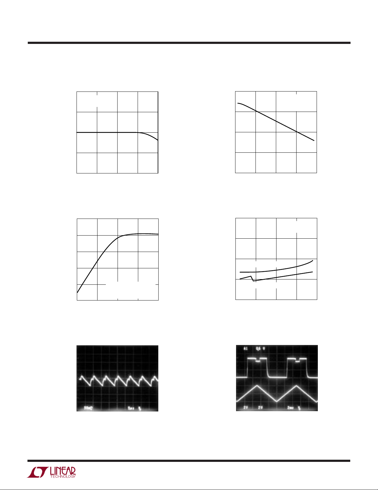
TYPICAL PERFORMANCE CHARACTERISTICS
Output Voltage vs Output Current
(3V Mode)
3.10
3.05
VIN = V
T
A
= 25°C
MODE
= 3V
Efficiency vs Input Voltage
100
80
LTC1986
I
= 10mA
OUT
V
= 5V
OUT
= 25°C
T
A
3.00
OUTPUT VOLTAGE (V)
2.95
2.90
0.001
0.01
OUTPUT CURRENT (mA)
0.1
Efficiency vs Output Current
100
80
60
40
EFFICIENCY (%)
20
0
0.001
VIN = 3V
5V MODE (V
T
= 25°C
A
0.01
0.1
OUTPUT CURRENT (mA)
MODE
1
1986 G01
= 0.6VIN)
1
1986 G03
60
EFFICIENCY (%)
40
20
10
2.5
3.0
3.5
INPUT VOLTAGE (V)
4.0
4.5
1986 G02
Positive Supply Current vs
Input Voltage
40
30
20
5V MODE (V
10
0
3V MODE (V
2.5
POSITIVE SUPPLY CURRENT (mA )
10
MODE
MODE
3.0
INPUT VOLTAGE (V)
= 0.6VIN)
= VIN)
3.5
I
OUT
T
A
= 0mA
= 25°C
4.0
4.5
1986 G04
V
OUT
50mV/DIV
AC COUPLED
Output Voltage Ripple
(5V Mode)
= 3V
V
IN
= 10mA
I
OUT
T
= 25°C 1986 G05
A
5ms/DIV
V
OUT
2V/DIV
V
MODE
2V/DIV
Output Voltage vs
V
Waveforms
MODE
5V
0V
4V
0V
= 4V
V
IN
= 25°C 1986 G06
T
A
2ms/DIV
3
 Loading...