

Linear Technology LTC1985-1.8 Datasheet
Final Electrical Specifications
FEATURES
LTC1985-1.8
Micropower Precision
Triple Supply Monitor
with Push-Pull Reset Output
in a 5-Lead SOT-23 Package
March 2000
U
DESCRIPTIO
■
Monitors Three Inputs Simultaneously:
3V, 1.8V and Adjustable
■
±1.5% Threshold Accuracy Over Temperature
■
Very Low Supply Current: 10µA Typ
■
200ms Reset Time Delay
■
Power Supply Glitch Immunity
■
Guaranteed RESET for V
■
3V Active-Low Push-Pull Reset Output
■
5-Lead SOT-23 Package
≥ 1V or V
CC3
CC18
U
APPLICATIO S
■
Desktop Computers
■
Notebook Computers
■
Intelligent Instruments
■
Portable Battery-Powered Equipment
■
Network Servers
U
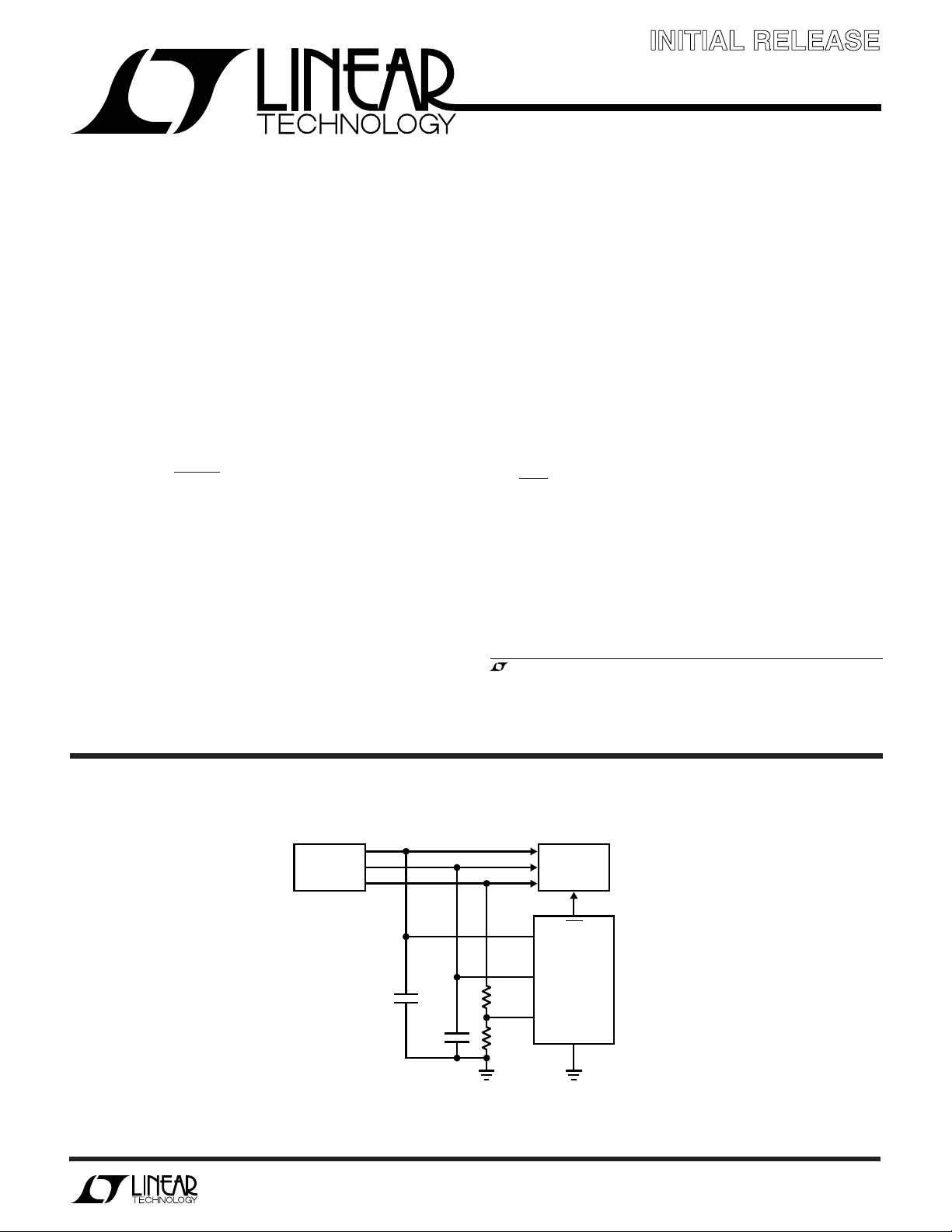
TYPICAL APPLICATIO
≥ 1V
The LTC®1985-1.8 is a triple supply monitor intended for
systems with multiple supply voltages. The reset output
remains low until all three supplies have been in compliance for 200ms. Tight 1.5% accuracy specifications and
glitch immunity ensure reliable reset operation without
false triggering.
The RST output is guaranteed to be in the correct state for
V
CC18
or V
down to 1V. The LTC1985 may also be
CC3
configured to monitor any one or two VCC inputs instead
of three, depending on system requirements.
Very low (10µA typical) supply current makes the LTC1985
ideal for power conscious systems.
The LTC1985 is available in a 5-lead SOT-23 package.
, LTC and LT are registered trademarks of Linear Technology Corporation.
3V
DC/DC
CONVERTER
Information furnished by Linear Technology Corporation is believed to be accurate and reliable.
However, no responsibility is assumed for its use. Linear Technology Corporation makes no representation that the interconnection of its circuits as described herein will not infringe on existing patent rights.
1.8V
2.5V
0.1µF
0.1µF
R1
130k
1%
R2
100k
1%
5
V
CC3
LTC1985-1.8
4
V
CC18
3
V
CCA
SYSTEM
LOGIC
1
RST
GND
2
1985-1.8 TA01
1
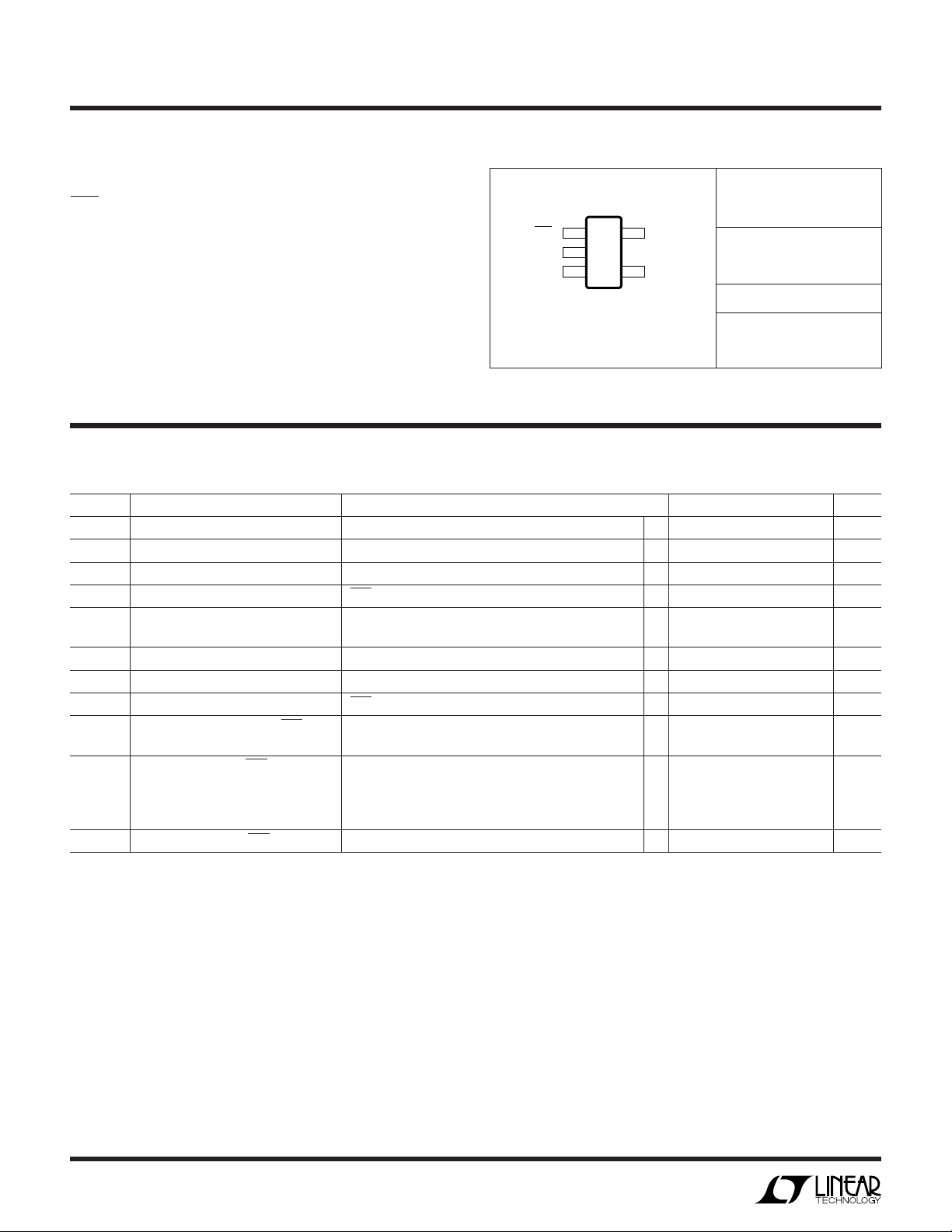
LTC1985-1.8
RST 1
GND 2
TOP VIEW
S5 PACKAGE
5-LEAD PLASTIC SOT-23
V
CCA
3
5 V
CC3
4 V
CC18
WWWU
ABSOLUTE AXI U RATI GS
PACKAGE/ORDER I FOR ATIO
UU
W
(Notes 1, 2)
V
, V
CC3
RST .......................................... –0.3V to (V
CC18
, V
...................................... –0.3V to 7V
CCA
CC3
+ 0.3V)
ORDER
PART NUMBER
Operating Temperature Range
(Note 3) ............................................. –40°C to 85°C
LTC1985ES5-1.8
Storage Temperature Range ................ –65°C to 150°C
Lead Temperature (Soldering, 10 sec)................ 300°C
T
= 125°C, θ
JMAX
Consult factory for Industrial and Military grade parts.
ELECTRICAL CHARACTERISTICS
temperature range, otherwise specificaitons are at TA = 25°C. V
SYMBOL PARAMETER CONDITIONS MIN TYP MAX UNITS
V
RT3
V
RT18
V
RTA
V
CCOP
I
VCC3
I
VCC18
I
VCCA
t
RST
t
UV
V
OL
V
OH
Reset Threshold V
Reset Threshold V
Reset Threshold V
V
, V
CC3
CC18
V
Supply Current V
CC3
V
Supply Current V
CC18
V
Input Current V
CCA
Reset Pulse Width RST Low ● 140 200 280 ms
VCC Undervoltage Detect to RST V
Output Voltage Low, RST I
Output Voltage High, RST I
CC3
CC18
CCA
Operating Voltage RST in Correct Logic State ● 17V
V
Input Threshold ● 2.760 2.805 2.850 V
CC3
V
CC18
V
Input Threshold ● 0.985 1.000 1.015 V
CCA
CC18
V
CC18
CC18
= 1V ● –15 0 15 nA
CCA
CC18
Threshold V
= 2.5mA, V
SINK
= 100µA, V
I
SINK
I
= 100µA, V
SINK
= 100µA, V
I
SINK
SOURCE
The ● denotes specifications which apply over the full operating
= 3V, V
CC3
Input Threshold ● 1.656 1.683 1.710 V
> V
CC3
< V
, V
CC3
< V
CC3
, V
CC3
= 200µA ● 0.8V
= 3V (Note 4) ● 10 20 µA
CC3
, V
= 1.8V (Note 4) ● 12 µA
CC18
or V
Less Than Reset 110 µs
CCA
by More Than 1%
RT
= 3V, V
CC3
CC3
CC3
CC3
= 1V, V
= 0V, V
= 1V, V
CC18
CC18
CC18
CC18
= 1.8V, V
CC18
= 0V ● 0.15 0.4 V
= 0V ● 0.05 0.3 V
= 1V ● 0.05 0.3 V
= 1V ● 0.05 0.3 V
JA
CCA
= 250°C/W
= V
unless otherwise noted.
CC3
● 12 µA
S5 PART MARKING
LTNM
CC3
V
Note 1: Absolute Maximum Ratings are those values beyond which the life
of the device may be impaired.
Note 2: All voltage values are with respect to GND.
Note 3: The LTC1985E is guaranteed to meet specified performance from
0°C to 70°C and is designed, characterized and assured to meet the
2
extended temperature limits of –40°C to 85°C but are not tested at these
temperatures.
Note 4: Both V
has the greatest potential.
CC3
and V
can act as the supply depending on which pin
CC18
UW
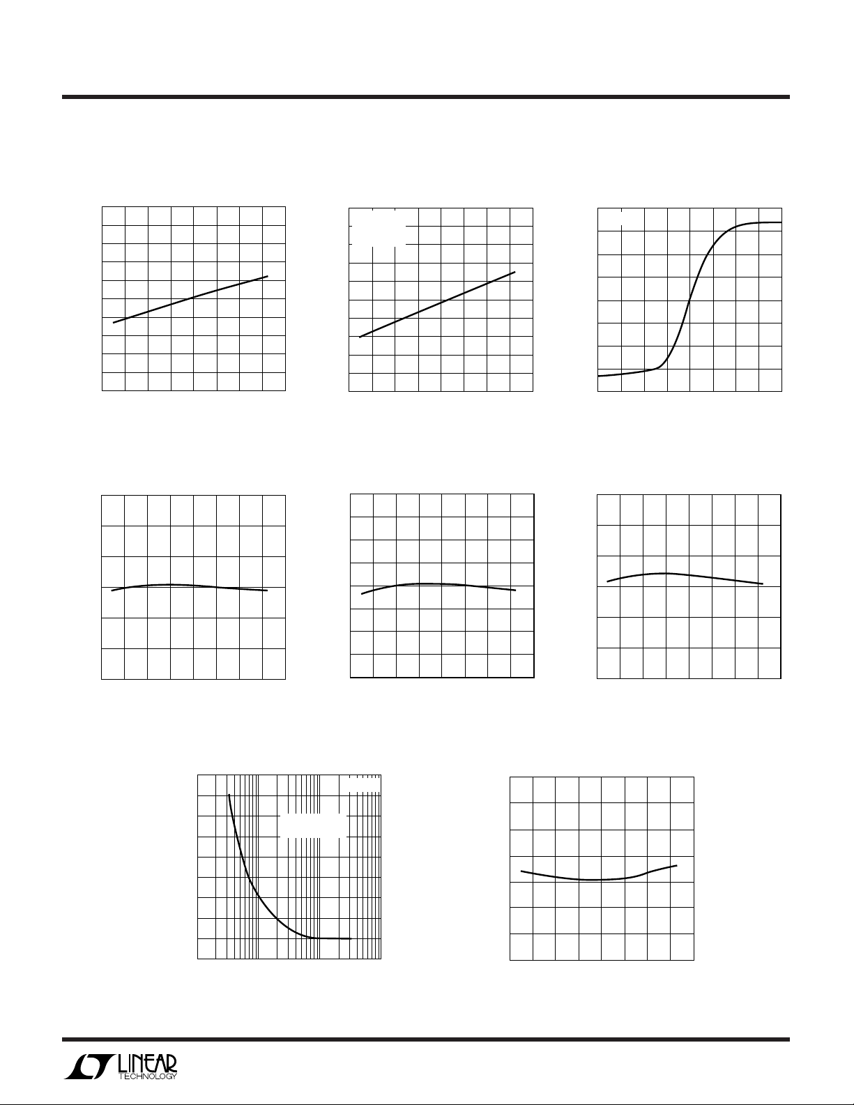
TYPICAL PERFOR A CE CHARACTERISTICS
I
I
vs Temperature
VCC3
15
14
13
12
11
(µA)
10
VCC3
I
9
8
7
6
5
–60
–40 0
–20
TEMPERATURE (°C)
V
Threshold Voltage
CCA
vs Temperature
1.015
(V)
1.010
RTA
1.005
1.000
0.995
THRESHOLD VOLTAGE, V
0.990
CCA
V
0.985
–60
–40 0
–20 20
TEMPERATURE (°C)
1.5
1.4
1.3
1.2
1.1
(µA)
1.0
VCC18
0.9
I
0.8
0.7
0.6
80
20
60
40
40
60
1985-18 G01
80
1985-18 G04
100
100
0.5
2.845
2.835
(V)
RT3
2.825
2.815
2.805
2.795
2.785
THRESHOLD VOLTAGE, V
CC3
2.775
V
2.765
vs Temperature
VCC18
V
= 3V
CC3
= 3V
V
CCA
= 1.8V
V
CC18
–60
–40 0
–20
TEMPERATURE (°C)
V
Threshold Voltage
CC3
vs Temperature
–60
–40 0
–20
TEMPERATURE (°C)
20
20
60
40
60
40
80
1985-18 G02
80
1985-18 G05
2.0
1.5
1.0
0.5
–0.5
INPUT CURRENT (nA)
–1.0
–1.5
100
100
–2.0
1.710
(V)
1.700
RT18
1.690
1.680
1.670
THRESHOLD VOLTAGE, V
1.660
CC18
V
1.650
LTC1985-1.8
V
Input Current
CCA
vs Input Voltage
TA = 25°C
0
0.80 0.85 0.95 1.05 1.15
0.90
V
Threshold Voltage
CC18
vs Temperature
–40 0
–60
–20 20
1
INPUT VOLTAGE (V)
40
TEMPERATURE (°C)
1.10
1985-18 G03
60
1985-18 G06
1.20
80
100
Typical Transient Duration
vs Comparator Overdrive
450
400
350
300
250
200
150
100
TYPICAL TRANSIENT DIRATION (µs)
50
0
0.1
RESET COMPARATOR OVERDRIVE VOLTAGE (% OF VCC)
RESET OCCURS
ABOVE CURVE
1 10 100
TA = 25°C
1985-18 G07
Reset Pulse Width
vs Temperature
280
260
(ms)
240
RST
220
200
180
RESET PULSE WIDTH, t
160
140
–60 –40
–20 20 40 800 100
TEMPERATURE (°C)
60
1985-18 G08
3
 Loading...