


FEATURES
LTC1960
Dual Battery Charger/
Selector with SPI Interface
U
DESCRIPTIO
■
Complete Dual-Battery Charger/Selector System
■
Serial SPI Interface Allows External µC Control and
Monitoring
■
Simultaneous Dual-Battery Discharge Extends Run
Time by Typically 10%
■
Simultaneous Dual-Battery Charging Reduces
Charging Time by Up to 50%
■
Automatic PowerPathTM Switching in <10µs
Prevents Power Interruption
■
Circuit Breaker Protects Against Overcurrent Faults
■
5% Accurate Adapter Current Limit Maximizes
Charging Rate*
■
95% Efficient Synchronous Buck Charger
■
Charger Has Low 0.5V Dropout Voltage
■
No Audible Noise Generation, Even with Ceramic
Capacitors
■
11-Bit VDAC Delivers 0.8% Voltage Accuracy
■
10-Bit IDAC Delivers 5% Current Accuracy
■
VIN Up to 32V; V
■
Available in 5mm × 7mm 38-Pin QFN and 36-Pin
Up to 28V
BATT
Narrow SSOP Packages
U
APPLICATIO S
■
Portable Computers
■
Portable Instruments
The LTC®1960 is a highly-integrated battery charger and
selector intended for portable products using dual smart
batteries. A serial SPI interface allows an external
microcontroller to control and monitor status of both
batteries.
A proprietary PowerPath architecture supports simultaneous charging or discharging of both batteries. Typical
battery run times are extended by 10%, while charging
times are reduced by up to 50%. The LTC1960 automatically switches between power sources in less than 10µs to
prevent power interruption upon battery or wall adapter
removal.
The synchronous buck battery charger delivers 95%
efficiency with only 0.5V dropout voltage, and prevents
audible noise in all operating modes. Patented* input
current limiting with 5% accuracy charges batteries in the
shortest possible time without overloading the wall adapter.
The LTC1960’s 5mm × 7mm 38-pin QFN and 36-pin
narrow SSOP packages allow implementation of a complete SBS-compliant dual battery system while consuming minimum PCB area.
, LT, LTC and LTM are registered trademarks of Linear Technology Corporation.
PowerPath is a trademark of Linear Technology Corporation.
All other trademarks are the property of their respective owners.
*Protected by U.S. Patents, including 5481178, 5723970, 6304066, 6580258.
TYPICAL APPLICATIO
LTC1960 Dual Battery/Selector System Architecture
DC
IN
BAT2 BAT1
U
SYSTEM POWER
LTC1960 MICROCONTROLLER
4
SPI
SMBus
1960 TA01
Dual vs Sequential Charging
3500
3000
2500
2000
1500
1000
500
0
3500
3000
2500
2000
BATTERY CURRENT (mA)
1500
1000
500
0
0
BATTERY TYPE: 10.8V Li-Ion (MOLTECH NI2020)
REQUESTED CURRENT = 3A
REQUESTED VOLTAGE = 12.3V
MAX CHARGER CURRENT = 4.1A
BAT1
CURRENT
50
BAT1
CURRENT
100 150 200 250 300
TIME (MINUTES)
BAT2
CURRENT
BAT2
CURRENT
MINUTES
SEQUENTIAL
DUAL
100
1960 G10
1960fa
1
LTC1960
WW
W
ABSOLUTE AXI U RATI GS
Voltage from DCIN, SCP, SCN, CLP, V
PLUS
U
(Note 1)
,
SW to GND ................................................32V to – 0.3V
Voltage from SCH1, SCH2 to GND.............28V to –0.3V
Voltage from BOOST to GND .....................41V to –0.3V
PGND with Respect to GND .................................. ±0.3V
CSP, CSN, BAT1, BAT2 to GND ....................28V to – 5V
LOPWR, DCDIV to GND .............................10V to –0.3V
UUW
PACKAGE/ORDER I FOR ATIO
TOP VIEW
LOPWR
GB2I
GB2O
GB1I
GB1O
GDCI
GDCO
38 37 36 35 34 33 32
1V
SET
I
2
TH
I
3
SET
GND
4
DCDIV
5
SSB
6
SCK
7
MISO
8
MOSI
9
GND
10
CSN
11
CSP
12
13 14 15 16
CLP
38-LEAD (5mm × 7mm) PLASTIC QFN
T
THE EXPOSED PAD (PIN 39) IS GND. MUST BE SOLDERED TO THE PCB.
JMAX
39
17 18 19
CC
V
PGND
BGATE
COMP1
UHF PACKAGE
= 125°C, θJA = 34°C/W
UHF PART MARKING
LTC1960CUHF
Order Options Tape and Reel: Add #TR
Lead Free: Add #PBF Lead Free Tape and Reel: Add #TRPBF
Lead Free Part Marking: http://www.linear.com/leadfree/
Consult LTC Marketing for parts specified with wider operating temperature ranges.
DCIN
SW
31
SCP
SCN
30
BAT1
29
BAT2
28
V
27
GND
26
SCH2
25
GCH2
24
GCH1
23
22
SCH1
21
TGATE
20
BOOST
1960
PLUS
SSB, SCK, MOSI, MISO to GND................... 7V to –0.3V
COMP1 to GND ............................................ 5V to –0.3V
Operating Ambient Temperature
Range (Note 7) ........................................0°C to 70°C
Operating Junction Temperature .......... –40°C to 125°C
Storage Temperature ............................ –65°C to 185°C
Lead Temperature (Soldering, 10 sec).................. 300°C
TOP VIEW
V
PLUS
BAT2
BAT1
SCN
SCP
GDCO
GDCI
GB1O
GB1I
GB2O
GB2I
LOPWR
V
SET
I
I
SET
GND
DCDIV
SSB
1
2
3
4
5
6
7
8
9
10
11
12
13
14
TH
15
16
17
18
G PACKAGE
36-LEAD PLASTIC SSOP
T
= 125°C, θJA = 95°C/ W
JMAX
36
35
34
33
32
31
30
29
28
27
26
25
24
23
22
21
20
19
SCH2
GCH2
GCH1
SCH1
TGATE
BOOST
SW
DCIN
V
CC
BGATE
PGND
COMP1
CLP
CSP
CSN
MOSI
MISO
SCK
ORDER PART NUMBER
LTC1960CG
ELECTRICAL CHARACTERISTICS
temperature range (Note 7), otherwise specifications are at T
The ● denotes specifications which apply over the full operating
= 25°C.
V
A
DCIN
= 20V, V
BAT1
= 12V, V
= 12V unless otherwise noted.
BAT2
SYMBOL PARAMETER CONDITIONS MIN TYP MAX UNITS
Supply and Reference
DCIN Operating Range DCIN Selected 6 28 V
I
CH
DCIN Operating Current Not Charging (DCIN Selected) 1 1.5 mA
Charging (DCIN Selected) 1.3 2 mA
1960fa
2
LTC1960
ELECTRICAL CHARACTERISTICS
temperature range (Note 7), otherwise specifications are at T
The ● denotes specifications which apply over the full operating
= 25°C.
V
A
DCIN
= 20V, V
BAT1
= 12V, V
= 12V unless otherwise noted.
BAT2
SYMBOL PARAMETER CONDITIONS MIN TYP MAX UNITS
Supply and Reference
Battery Operating Voltage Range Battery Selected, PowerPath Function (Note 2) 6 28 V
Battery Drain Current Battery Selected, Not Charging, V
V
Diodes Forward Voltage:
PLUS
V
V
V
V
FDC
FB1
FB2
FSCN
DCIN to V
BAT1 to V
BAT2 to V
SCN to V
PLUS
PLUS
PLUS
PLUS
UVLO Undervoltage Lockout Threshold V
UVHYS UV Lockout Hysteresis V
V
VCC
V
LDR
VCC Regulator Output Voltage 5 5.2 5.4 V
VCC Load Regulation I
I
= 10mA 0.8 V
VCC
I
= 0mA 0.7 V
VCC
I
= 0mA 0.7 V
VCC
I
= 0mA 0.7 V
VCC
Ramping Down, Measured at V
PLUS
Rising, Measured at V
PLUS
= 0mA to 10mA 0.2 1 %
VCC
= 0V 175 µA
DCIN
to GND
PLUS
to GND 60 mV
PLUS
●
3 3.5 3.9 V
Switching Regulator
V
I
f
f
TOL
TOL
0SC
DO
Overall Voltage Accuracy 5V ≤ V
Overall Current Accuracy IDAC Value = 3FF
V
< 25V, (Note 3) –0.8 0.8 %
CSP
, V
OUT
CSN
HEX
= 12V
●
–1 1 %
–5 5 %
●
–6 6 %
Regulator Switching Frequency 255 300 345 kHz
Regulator Switching Frequency in Low Duty Cycle ≥99% 20 25 kHz
Dropout Mode
DC
I
MAX
I
SNS
MAX
Regulator Maximum Duty Cycle 99 99.5 %
Maximum Current Sense Threshold V
CA1 Input Bias Current V
= 2.2V 140 155 190 mV
ITH
= V
CSP
> 5V 150 µA
CSN
CMSL CA1/I1 Input Common Mode Low 0 V
CMSH CA1/I1 Input Common Mode High V
V
CL1
CL1 Turn-On Threshold 95 100 105 mV
–0.2 V
DCIN
TGATE Transition Time:
TG t
TG t
r
f
TGATE Rise Time C
TGATE Fall Time C
= 3300pF, 10% to 90% 50 90 ns
LOAD
= 3300pF, 10% to 90% 50 90 ns
LOAD
BGATE Transition Time:
BG t
BG t
r
f
BGATE Rise Time C
BGATE Fall Time C
= 3300pF, 10% to 90% 50 90 ns
LOAD
= 3300pF, 10% to 90% 40 80 ns
LOAD
Trip Points
V
V
I
V
V
V
BVT
TR
THYS
TSC
FTO
OVSD
DCDIV/LOPWR Threshold V
DCDIV/LOPWR Hysteresis Voltage V
DCDIV/LOPWR Input Bias Current V
Short-Circuit Comparator Threshold V
Fast Power Path Turn-Off Threshold V
Overvoltage Shutdown Threshold as a V
or V
DCDIV
or V
DCDIV
or V
DCDIV
– V
SCP
SCN
Rising from V
DCDIV
Rising from 0.8V until TGATE and BGATE 107 %
SET
Falling
LOPWR
Rising 30 mV
LOPWR
= 1.19V 20 200 nA
LOPWR
, V
≥ 5V
CC
CC
●
1.166 1.19 1.215 V
●
90 100 115 mV
6 7 7.9 V
Percent of Programmed Charger Voltage Stop Switching
DACs
I
RES
IDAC Resolution Guaranteed Monotonic Above I
/16 10 bits
MAX
IDAC Pulse Period:
t
IP
t
ILOW
Normal Mode 61015 µs
Low Current Mode 50 ms
1960fa
3
LTC1960
ELECTRICAL CHARACTERISTICS
temperature range (Note 7), otherwise specifications are at T
The ● denotes specifications which apply over the full operating
= 25°C.
V
A
DCIN
= 20V, V
BAT1
= 12V, V
= 12V unless otherwise noted.
BAT2
SYMBOL PARAMETER CONDITIONS MIN TYP MAX UNITS
DACs
V
V
V
t
RES
STEP
OFF
VP
VDAC Resolution Guaranteed Monotonic (5V < V
< 25V) 11 bits
BAT
VDAC Granularity 16 mV
VDAC Offset (Note 6) 0.8 V
VDAC Pulse Period 7 11 16.5 µs
Charge Mux Switches
t
ONC
t
OFFC
V
CON
V
COFF
V
TOC
V
FC
I
OC(SRC)
I
OC(SNK)
V
CHMIN
GCH1/GCH2 Tur-On Time V
GCH1/GCH2 Turn-Off Time V
CH Gate Clamp Voltage I
GCH1 V
GCH2 V
CH Gate Off Voltage I
GCH1 V
GCH2 V
CH Switch Reverse Turn-Off Voltage V
CH Switch Forward Regulation Voltage V
GCH1/GCH2 Active Regulation: V
GCHX
GCHX
V
CSN
LOAD
LOAD
CSN
BATX
GCHX
– V
– V
< V
BATX
= 1µA
GCH1
GCH2
=10µA
GCH1
GCH2
– V
BATX,
– V
– V
> 3V, V
SCHX
< 1V, from Time of 3 7 µs
SCHX
– 30mV, V
– V
SCH1
– V
SCH2
– V
SCH1
– V
SCH2
5V ≤ V
5V ≤ V
CSN,
= 1.5V
SCHX
SCHX
BATX
BATX
= TBD, C
= TBD, C
SCHX
≤ 28V
≤ 28V
= 3nF 5 10 ms
LOAD
= 3nF
LOAD
5 5.8 7 V
5 5.8 7 V
–0.8 –0.4 0 V
–0.8 –0.4 0 V
●
52040 mV
●
15 35 60 mV
Max Source Current –2 µA
Max Sink Current 2 µA
BATX Voltage Below Which 3.5 4.7 V
Charging is Inhibited (Does Not Apply
to Low Current Mode)
PowerPath Switches
t
DLY
t
PPB
t
ONPO
Blanking Period after UVLO Trip Switches Held Off 250 ms
Blanking Period after LOPWR Trip Switches in 3-Diode Mode 1 sec
GB1O/GB2O/GDCO Turn-On Time VGS < –3V, from Time of Battery/DC
●
510 µs
Removal, or LOPWR Indication
t
OFFPO
GB1O/GB2O/GDCO Turn-Off Time VGS > –1V, from Time of Battery/DC
●
37 µs
Removal, or LOPWR Indication
V
PONO
V
POFFO
V
TOP
V
FP
Output Gate Clamp Voltage I
LOAD
GB1O Highest (V
GB2O Highest (V
GDCO Highest (V
Output Gate Off Voltage I
LOAD
GB1O Highest (V
GB2O Highest (V
GDCO Highest (V
PowerPath Switch Reverse V
SCP
– V
Turn-Off Voltage 6V ≤ V
PowerPath Switch Forward V
BATX
Regulation Voltage 6V ≤ V
= 1µA
= –25µA
BATX
≤ 28V
SCP
– V
SCP
≤ 28V
SCP
BAT1
BAT2
DCIN
BAT1
BAT2
DCIN
or V
or V
or V
or V
or V
or V
or V
or V
SCP
DCIN
SCP
SCP
SCP
SCP
SCP
SCP
– V
– V
) – V
) – V
) – V
) – V
) – V
) – V
DCIN
SCP
GB1O
GB2O
GDCO
GB1O
GB2O
GDCO
4.75 6.25 7 V
4.75 6.25 7 V
4.75 6.25 7 V
0.18 0.25 V
0.18 0.25 V
0.18 0.25 V
●
52060 mV
●
02550 mV
GDCI/GB1I/GB2I Active Regulation (Note 4)
I
OP(SRC)
I
OP(SNK)
Source Current –4 µA
Sink Current 75 µA
4
1960fa
LTC1960
ELECTRICAL CHARACTERISTICS
temperature range (Note 7), otherwise specifications are at T
The ● denotes specifications which apply over the full operating
= 25°C.
V
A
DCIN
= 20V, V
BAT1
= 12V, V
= 12V unless otherwise noted.
BAT2
SYMBOL PARAMETER CONDITIONS MIN TYP MAX UNITS
t
ONPI
t
OFFPI
V
PONI
V
POFFI
Gate B1I/B2I/DCI Turn-On Time VGS < –3V, C
Gate B1I/B2I/DCI Turn-Off Time VGS > –1V, C
Input Gate Clamp Voltage I
GB1I Highest (V
GB2I Highest (V
GDCI Highest (V
Input Gate Off Voltage I
GB1I Highest (V
GB2I Highest (V
GDCI Highest (V
LOAD
LOAD
= 1µA
BAT1
BAT2
DCIN
= –25µA
BAT1
BAT2
DCIN
= 3nF (Note 5) 300 µs
LOAD
= 3nF (Note 5) 10 µs
LOAD
or V
or V
or V
or V
or V
or V
SCP
SCP
SCP
SCP
SCP
SCP
) – V
) – V
) – V
) – V
) – V
) – V
GB1I
GB2I
GDCI
GB1I
GB2I
GDCI
4.75 6.7 7.5 V
4.75 6.7 7.5 V
4.75 6.7 7.5 V
0.18 0.25 V
0.18 0.25 V
0.18 0.25 V
Logic I/O
IIH/I
V
IL
V
IH
V
OL
I
OFF
IL
SSB/SCK/MOSI Input High/Low Current
SSB/MOSI/SCK Input Low Voltage
SSB/MOSI/SCK Input High Voltage
MISO Output Low Voltage IOL = 1.3mA
MISO Output Off-State Leakage Current V
MISO
= 5V
●
–1 1 µA
●
●
2V
●
●
0.8 V
0.4 V
2 µA
SPI Timing (See Timing Diagram)
T
WD
t
SSH
t
CYC
t
SH
t
SL
t
LD
t
LG
t
su
t
H
t
A
t
dis
t
V
t
HO
t
Ir
t
If
t
Of
Note 1: Stresses beyond those listed under Absolute Maximum Ratings
may cause permanent damage to the device. Exposure to any Absolute
Maximum Rating condition for extended periods may affect device
reliability and lifetime.
Note 2. Battery voltage must be adequate to drive gates of PowerPath
P-channel FET switches. This does not affect charging voltage of the
battery, which can be zero volts.
Note 3. See Test Circuit.
Note 4. DCIN, BAT1, BAT2 are held at 12V and GDCI, GB1I, GB2I are
Watch Dog Timer
●
1.2 2.5 4.5 sec
SSB High Time 680 ns
SCK Period C
LOAD
= 200pF R
= 4.7k on MISO
PULLUP
●
2 µs
SCK High Time 680 ns
SCK Low Time 680 ns
Enable Lead Time 200 ns
Enable Lag Time 200 ns
Input Data Set-Up Time
Input Data Hold Time
Access Time (From Hi-Z to Data Active on MISO)
Disable Time (Hold Time to Hi-Z State on MISO)
Output Data Valid CL = 200pF, R
Output Data Hold
= 4.7k on MISO
PULLUP
●
100 ns
●
100 ns
●
●
●
●
0ns
125 ns
125 ns
580 ns
SCK/MOSI/SSB Rise Time 0.8V to 2V 250 ns
SCK/MOSI/SSB Fall Time 2V to 0.8V 250 ns
MISO Fall Time 2V to 0.4V, CL = 200 pF
●
400 ns
GB1I and GB2I. SCP is set at 11.9V to measure sink current at GDCI, GB1I
and GB2I.
Note 5. Extrapolated from testing with C
= 50pF.
L
Note 6. VDAC offset is equal to the reference voltage, since
= V
V
OUT
(16mV • VDAC
REF
(VALUE)
/2047 + 1).
Note 7. The LTC1960C is guaranteed to meet specified performance from
0°C to 70°C and is designed, characterized and expected to meet specified
performance at –40°C and 85°C, but is not tested at these extended
temperature limits.
forced to 10.5V. SCP is set at 12.0V to measure source current at GDCI,
1960fa
5
LTC1960
TIME (ms)
–4 –2
BAT1 VOLTAGE (V)
14
12
10
8
6
4
2
0
1960 G05
42
10 12 14 16
0
68
VIN = 20V
VDAC = 12.29V
IDAC = 3000mA
LOAD CURRENT = 1A
T
A
= 25°C
BAT1
OUTPUT
LOAD
CONNECTED
LOAD
DISCONNECTED
UW
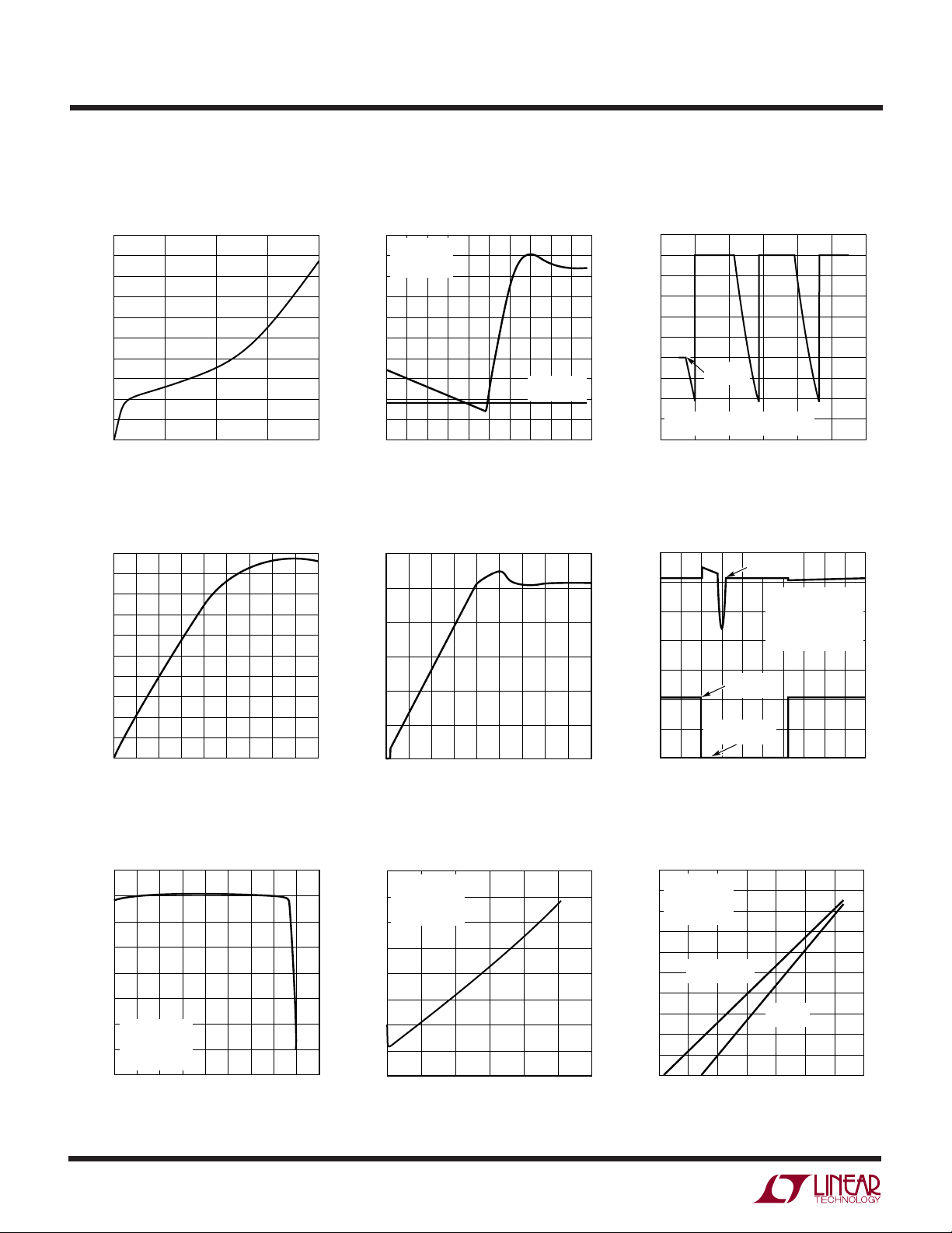
TYPICAL PERFOR A CE CHARACTERISTICS
Battery Drain Current
(BAT1 Selected)
250
TA = 25°C
240
230
220
210
200
190
180
BAT1 CURRENT (µA)
170
160
150
6
12
Charger Efficiency
100
90
80
70
60
50
40
EFFICIENCY (%)
30
20
10
0
0.025
0
18
BAT1 VOLTAGE (V)
0.50
0.10
I
(A)
OUT
Power Path Autonomous
Power Path Switching
16
C
= 20µF
LOAD
15
= 0.8A
I
LOAD
= 25°C
T
A
14
13
12
11
10
LOAD VOLTAGE (V)
9
8
7
24
30
1960 G01
6
–50 –40 –30
–20
–10
TIME (µs)
LOPWR
THRESHOLD
10 20 30 40 50
0
1960 G02
Charger Start-Up
12
10
8
6
4
CHARGER OUTPUT (V)
2
2.5 4.0
1960 G14
0
–0.05
0 0.10
0.05
0.30
0.20 0.40
0.25
0.15
TIME (SEC)
0.35
1960 G04
Switching
16
15
14
13
12
11
10
LOAD VOLTAGE (V)
9
8
7
6
BAT1
REMOVED
NOTE: LIGHT LOAD TO
EXAGGERATE SWITCHING EVENT
–1
0
1
Charger Load Dump
23
TIME (SEC)
4
5
1960 G03
6
Charger Load Regulation
12.4
12.3
12.2
12.1
12.0
11.9
BAT1 VOLTAGE (V)
11.8
11.7
11.6
VIN = 20V
VDAC = 12.288V
IDAC = 4000mA
= 25°C
T
A
1000 2000 3000
0
CHARGE CURRENT (mA)
4000
1960 G06
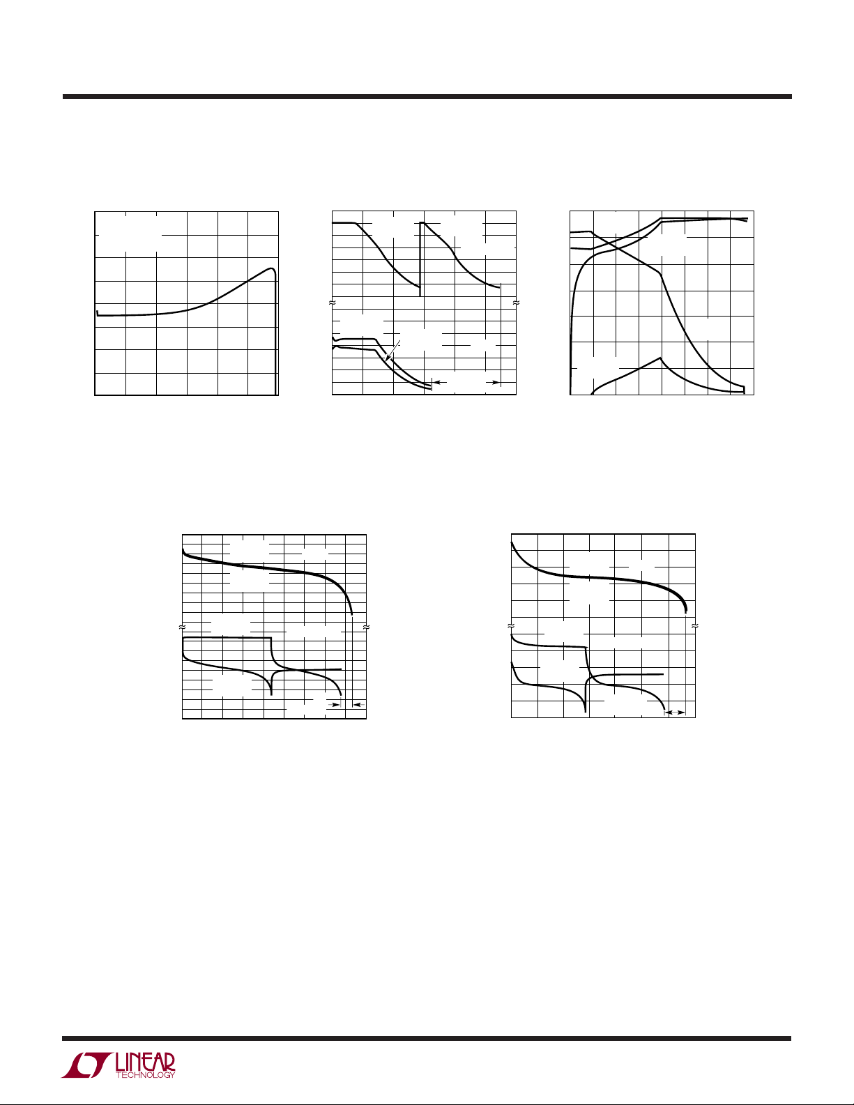
Charging Current Accuracy
120
V
= 20V
DCIN
= 12V
V
BAT1
100
OUTPUT CURRENT ERROR (mA)
–20
–40
80
60
40
20
0
0 200
R
SNS
= 25°C
T
A
= 0.025Ω
400 800600
IDAC VALUE
1000
1200
1960 G07
IDAC Low Current Mode vs
Normal Mode
500
VIN = 20V
450
400
350
300
250
200
150
CHARGING CURRENT (mA)
100
50
= 12V
V
BAT1
= 0.025Ω
R
SNS
= 25°C
T
A
LOW CURRENT
MODE
0
0
160
80
PROGRAMMED CURRENT (mA)
240
NORMAL
MODE
320
400
480
560
1960 G08
1960fa
UW
BAT2
VOLTAGE
BAT2
CURRENT
BAT1
CURRENT
BAT1
VOLTAGE
BAT1 INITIAL CAPACITY = 0%
BAT2 INITIAL CAPACITY = 90%
PROGRAMMED CHARGER CURRENT = 3A
PROGRAMMED CHARGER VOLTAGE = 16.8V
TIME (MINUTES)
0
BATTERY VOLTAGE (V)
120
1960 G11
40 80 160
17.0
16.5
16.0
15.5
15.0
14.5
14.0
13.5
20 60 100 140
BATTERY CURRENT (mA)
3500
3000
2500
2000
1500
1000
500
0
TYPICAL PERFOR A CE CHARACTERISTICS
Voltage Accuracy
100
DCIN = 24V
= 25°C
T
A
75
50
25
–25
–50
OUTPUT VOLTAGE ERROR (mV)
–75
–100
I
LOAD
0
250 450
= 100mA
650 1050850
VDAC VALUE
1250
1450
1960 G09
Dual vs Sequential Charging
3500
3000
2500
2000
1500
1000
500
0
3500
3000
2500
2000
BATTERY CURRENT (mA)
1500
1000
500
0
0
BATTERY TYPE: 10.8V Li-Ion (MOLTECH NI2020)
REQUESTED CURRENT = 3A
REQUESTED VOLTAGE = 12.3V
MAX CHARGER CURRENT = 4.1A
BAT1
CURRENT
50
BAT1
CURRENT
100 150 200 250 300
TIME (MINUTES)
BAT2
CURRENT
BAT2
CURRENT
MINUTES
SEQUENTIAL
DUAL
100
LTC1960
Dual Charging Batteries with
Different Charge State
1960 G10
12.0
11.0
10.0
9.0
8.0
12.0
11.0
BATTERY VOLTAGE (V)
10.0
9.0
8.0
Dual vs Sequential Discharge
BAT1
VOLTAGE
BAT2
VOLTAGE
BAT2
VOLTAGE
BAT1
VOLTAGE
60 80 100 140
20 180
0
40
TIME (MINUTES)
BATTERY TYPE: 10.8V Li-Ion(MOLTECH NI2020)
LOAD CURRENT = 3A
DUAL
SEQUENTIAL
11
MINUTES
120
160
1960 G12
Dual vs Sequential Discharge
15
14
13
12
11
10
15
14
13
BATTERY VOLTAGE (V)
12
11
10
20
0
BATTERY TYPE: 12V NIMH (MOLTECH NJ1020)
LOAD: 33W
BAT2
VOLTAGE
BAT1
VOLTAGE
40
TIME (MINUTES)
BAT2
VOLTAGE
BAT1
VOLTAGE
60 80 100 140
DUAL
SEQUENTIAL
MINUTES
16
120
1960 G13
1960fa
7

LTC1960
PIN FUNCTIONS
UUU
(G/UHF)
Input Power Related
SCN (Pin 4/Pin 30): PowerPath Current Sensing Negative
Input. This pin should be connected directly to the “bottom” (output side) of the low valued resistor in series with
the three PowerPath switch pairs, for detecting shortcircuit current events. Also powers LTC1960 internal
circuitry when all other sources are absent.
SCP (Pin 5/Pin 31): PowerPath Current Sensing Positive
Input. This pin should be connected directly to the “top”
(switch side) of the low valued resistor in series with the
three PowerPath switch pairs, for detecting short-circuit
current events.
GDCO (Pin 6/Pin 32): DCIN Output Switch Gate Drive.
Together with GDCI, this pin drives the gate of the Pchannel switch in series with the DCIN input switch.
GDCI (Pin 7/Pin 33): DCIN Input Switch Gate Drive.
Together with GDCO, this pin drives the gate of the Pchannel switch connected to the DCIN input.
GB1O (Pin 8/Pin 34): BAT1 Output Switch Gate Drive.
Together with GB1I, this pin drives the gate of the Pchannel switch in series with the BAT1 input switch.
GB1I (Pin 9/Pin 35): BAT1 Input Switch Gate Drive.
Together with GB1O, this pin drives the gate of the Pchannel switch connected to the BAT1 input.
GB2O (Pin 10/Pin 36): BAT2 Output Switch Gate Drive.
Together with GB2I, this pin drives the gate of the Pchannel switch in series with the BAT2 input switch.
GB2I (Pin 11/Pin 37): BAT2 Input Switch Gate Drive.
Together with GB2O, this pin drives the gate of the Pchannel switch connected to the BAT2 input.
CLP (Pin 24/Pin 13): This is the Positive Input to the
Supply Current Limiting Amplifier CL1. The threshold is
set at 100mV above the voltage at the DCIN pin. When
used to limit supply current, a filter is needed to filter out
the switching noise.
Battery Charging Related
V
(Pin 13/Pin 1): The Tap Point of a Programmable
SET
Resistor Divider which Provides Battery Voltage Feedback
to the Charger. A capacitor from CSN to V
V
to GND provide necessary compensation and filter-
SET
ing for the voltage loop.
(Pin 14/Pin 2): This is the Control Signal of the Inner
I
TH
Loop of the Current Mode PWM. Higher I
to higher charging current in normal operation. A capacitor of at least 0.1µF to GND filters out PWM ripple. Typical
full-scale output current is 30µA. Nominal voltage range
for this pin is 0V to 2.4V.
I
(Pin 15/Pin 3): A Capacitor from I
SET
Required to Filter Higher Frequency Components from the
Delta-Sigma IDAC.
CSN (Pin 22/Pin 11): Current Amplifier CA1 Input. Connect this to the common output of the charger MUX
switches.
CSP (Pin 23/Pin 12): Current Amplifier CA1 Input. This
pin and the CSN pin measure the voltage across the sense
resistor, RSNS, to provide the instantaneous current
signals required for both peak and average current mode
operation.
COMP1 (Pin 25/Pin 14): This is the Compensation Node
for the Amplifier CL1. A capacitor is required from this pin
to GND if input current amplifier CL1 is used. At input
adapter current limit, this node rises to 1V. By forcing
COMP1 low, amplifier CL1 will be defeated (no adapter
current limit). COMP1 can source 10µA.
BGATE (Pin 27/Pin 16): Drives the Bottom External MOSFET
of the Battery Charger Buck Converter.
SW (Pin 30/Pin 19): Connected to Source of Top External
MOSFET Switch. Used as reference for top gate driver.
BOOST (Pin 31/Pin 20): Supply to Topside Floating Driver.
The bootstrap capacitor is returned to this pin. Voltage
swing at this pin is from a diode drop below VCC to (DCIN
+ VCC).
and one from
SET
corresponds
TH
to Ground is
SET
8
1960fa
 Loading...