

Linear Technology LTC1929 Datasheet
LTC1929
Final Electrical Specifications
2-Phase, High Efficiency,
Synchronous Step-Down
Switching Regulator
FEATURES
■
2-Phase Single Output Controller
■
Reduces Required Input Capacitance and Power
Supply Induced Noise
■
Current Mode Control Ensures Current Sharing
■
Phase-Lockable Fixed Frequency: 150kHz to 300kHz
■
True Remote Sensing Differential Amplifier
■
OPTI-LOOPTM Compensation Improves Transient
Response
■
±
1% Output Voltage Accuracy
■
Wide VIN Range: 4V to 36V Operation
■
Very Low Dropout Operation: 99% Duty Cycle
■
Adjustable Soft-Start Current Ramping
■
Internal Current Foldback
■
Short-Circuit Shutdown Timer with Defeat Option
■
Overvoltage Soft-Latch Eliminates Nuisance Trips
■
Available in 28-Lead SSOP Package
U
APPLICATIO S
■
Desktop Computers
■
Internet/Network Servers
■
Large Memory Arrays
■
DC Power Distribution Systems
U
August 1999
DESCRIPTIO
The LTC®1929 is a 2-phase, single output, synchronous
step-down current mode switching regulator controller
that drives N-channel external power MOSFET stages in a
phase-lockable fixed frequency architecture. The 2-phase
controller drives its two output stages out of phase at
frequencies up to 300kHz to minimize the RMS ripple
currents in both input and output capacitors. The 2-phase
technique effectively multiplies the fundamental frequency
by two, improving transient response while operating
each channel at an optimum frequency for efficiency.
Thermal design is also simplified.
An internal differential amplifier provides true remote
sensing of the regulated supply’s positive and negative
output terminals as required by high current applications.
The RUN/SS pin provides soft-start and a defeatable,
timed, latched short-circuit shutdown to shut down both
channels. Internal foldback current limit provides protection for the external sychronous MOSFETs in the event of
an output fault. OPTI-LOOP compensation allows the
transient response to be optimized over a wide range of
output capacitance and ESR values.
, LTC and LT are registered trademarks of Linear Technology Corporation.
OPTI-LOOP is a trademark of Linear Technology Corporation.
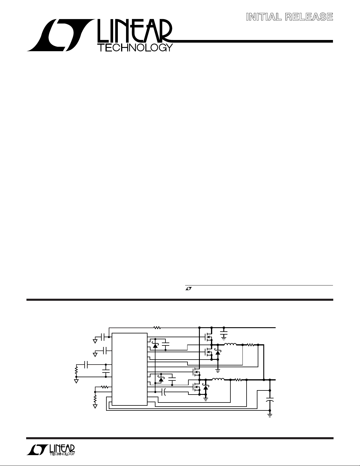
TYPICAL APPLICATIO
1000pF
10k
SS
8.06k
U
10Ω
1µH
10µF ×4
35V
CERAMIC
L1
1µH
D1
L2
0.002Ω
0.1µF
0.1µF
S
100pF
8.06k
S
C
OUT
L1, L2: CEPH149-1ROMC
S
V
IN
RUN/SS
I
TH
SGND
V
DIFFOUT
EAIN
–
V
OS
+
V
OS
: T510E108K004AS
LTC1929
BOOST1
PGND
SENSE1
SENSE1
BOOST2
INTV
SENSE2
SENSE2
TG1
SW1
BG1
TG2
SW2
BG2
S
0.47µF
S
+
–
S
S
S
CC
+
–
0.47µF
S
10µF
+
D2
Figure 1. High Current 2-Phase Step-Down Converter
Information furnished by Linear Technology Corporation is believed to be accurate and reliable.
However, no responsibility is assumed for its use. Linear Technology Corporation makes no representation that the interconnection of its circuits as described herein will not infringe on existing patent rights.
0.002Ω
+
V
IN
5V TO 28V
V
OUT
1.6V/40A
C
OUT
1000µF ×2
4V
1929 TA01
1
LTC1929
WW
W
U
ABSOLUTE AXI U RATI GS
(Note 1)
Input Supply Voltage (VIN).........................36V to –0.3V
Topside Driver Voltages (BOOST1,2).........42V to –0.3V
Switch Voltage (SW1, 2) .............................36V to –5 V
SENSE1+, SENSE2+, SENSE1–,
SENSE2– Voltages........................ (1.1)INTVCC to –0.3V
EAIN, V
RUN/SS, AMPMD Voltages..........................7V to –0.3V
Boosted Driver Voltage (BOOST-SW) ..........7V to –0.3V
PLLFLTR, PLLIN, V
ITH Voltage................................................2.7V to –0.3V
Peak Output Current <1µs(TGL1,2, BG1,2)................ 3A
INTVCC RMS Output Current................................ 50mA
Operating Ambient Temperature Range
LTC1929C.................................................. 0°C to 85°C
LTC1929I .............................................. – 40°C to 85°C
Junction Temperature (Note 2)............................. 125°C
Storage Temperature Range ................. –65°C to 150°C
Lead Temperature (Soldering, 10 sec)..................300°C
OS
+
–
, V
, EXTVCC, INTVCC,
OS
DIFFOUT
Voltages .... INTVCC to –0.3V
UUW
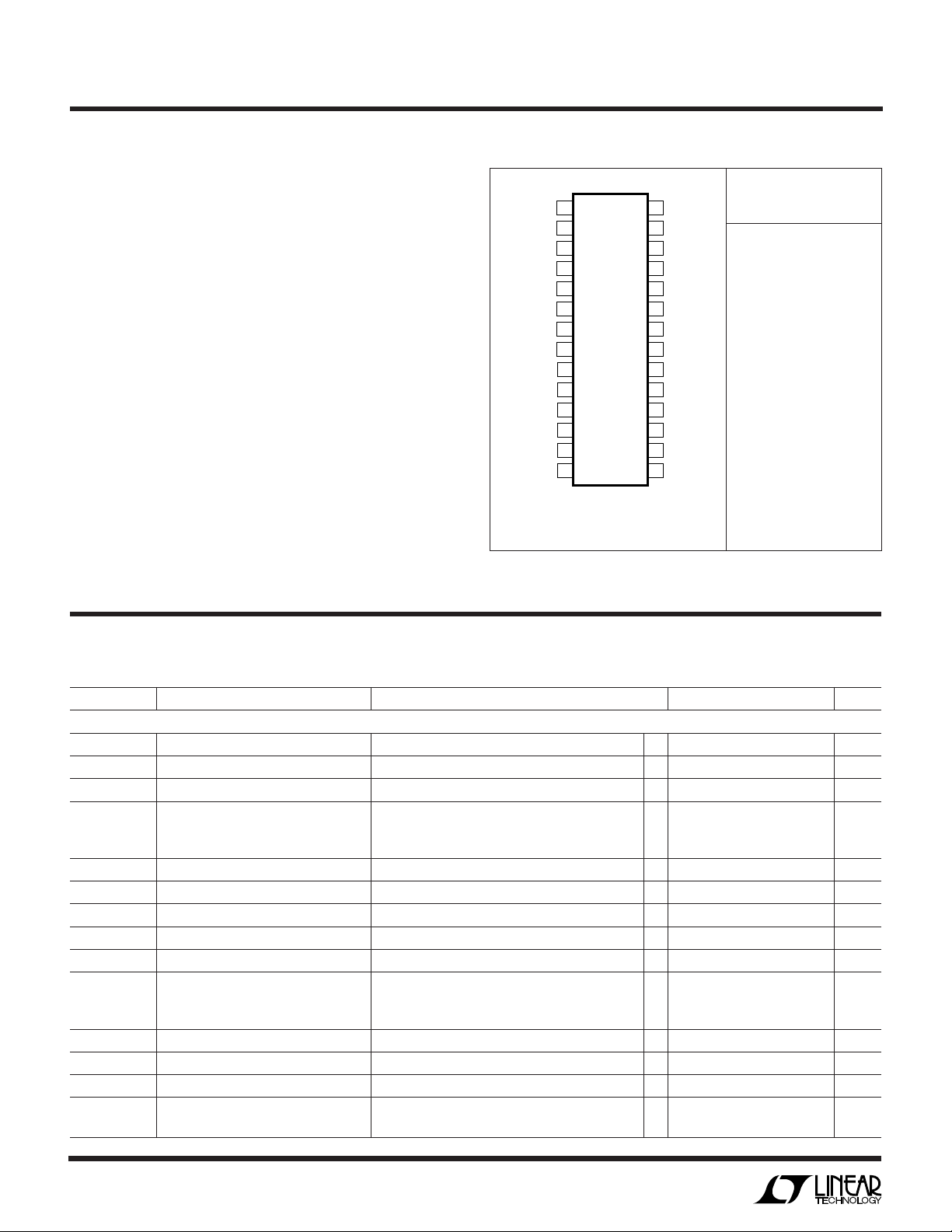
PACKAGE/ORDER I FOR ATIO
TOP VIEW
RUN/SS
SENSE1
SENSE1
EAIN
PLLFLTR
PLLIN
SGND
V
DIFFOUT
V
OS
V
OS
SENSE2
SENSE2
1
+
2
–
3
4
5
6
7
NC
8
I
TH
9
10
–
11
+
12
–
13
+
14
G PACKAGE
28-LEAD PLASTIC SSOP
T
= 125°C, θJA = 95°C/W
JMAX
28
27
26
25
24
23
22
21
20
19
18
17
16
15
NC
TG1
SW1
BOOST1
V
IN
BG1
EXTV
CC
INTV
CC
PGND
BG2
BOOST2
SW2
TG2
AMPMD
Consult factory for Military grade parts.
ORDER PART
NUMBER
LTC1929CG
LTC1929IG
ELECTRICAL CHARACTERISTICS
temperature range, otherwise specifications are at T
The ● denotes the specifications which apply over the full operating
= 25°C. V
A
= 15V, V
IN
= 5V unless otherwise noted.
RUN/SS
SYMBOL PARAMETER CONDITIONS MIN TYP MAX UNITS
Main Control Loop
V
EAIN
V
SENSEMAX
I
INEAIN
V
LOADREG
V
REFLNREG
V
OVL
Regulated Feedback Voltage (Note 3); ITH Voltage = 1.2V ● 0.792 0.800 0.808 V
Maximum Current Sense Threshold V
–
= 5V 65 75 85 mV
SENSE
Feedback Current (Note 3) –5 –50 nA
Output Voltage Load Regulation (Note 3)
Measured in Servo Loop; I
Measured in Servo Loop; I
Voltage = 0.7V 0.05 0.3 %
TH
Voltage = 2V –0.1 –0.5 %
TH
Reference Voltage Line Regulation VIN = 3.6V to 30V (Note 3) 0.002 %/V
Output Overvoltage Threshold Measured at V
EAIN
● 0.84 0.86 0.88 V
UVLO Undervoltage Lockout VIN Ramping Down 3 3.5 4 V
g
m
g
mOL
I
Q
I
RUN/SS
V
RUN/SS
V
RUN/SSLO
I
SCL
Transconductance Amplifier g
m
ITH = 1.2V; Sink/Source 5µA; (Note 3) 3 mmho
Transconductance Amplifier Gain ITH = 1.2V; (gmxZL; No Ext Load); (Note 3) 1.5 V/mV
Input DC Supply Current (Note 4)
Normal Mode EXTV
Shutdown V
Soft-Start Charge Current V
RUN/SS Pin ON Threshold V
RUN/SS Pin Latchoff Arming V
Tied to V
CC
= 0V 20 40 µA
RUN/SS
= 1.9V –1.2 µA
RUN/SS
Rising 1.0 1.5 1.9 V
RUN/SS
Rising from 3V 4.1 V
RUN/SS
RUN/SS Discharge Current Soft Short Condition V
= 4.5V
V
RUN/SS
OUT
; V
= 5V 470 µA
OUT
= 0.5V; 0.5 2.0 4.0 µA
EAIN
2
LTC1929
ELECTRICAL CHARACTERISTICS
temperature range, otherwise specifications are at T
The ● denotes the specifications which apply over the full operating
= 25°C. V
A
= 15V, V
IN
= 5V unless otherwise noted.
RUN/SS
SYMBOL PARAMETER CONDITIONS MIN TYP MAX UNITS
I
SDLHO
I
SENSE
DF
MAX
Shutdown Latch Disable Current V
Total Sense Pins Source Current Each Channel: V
= 0.5V 1.6 5 µA
EAIN
SENSE1–, 2
– = V
SENSE1+, 2
+ = 0V –60 µA
Maximum Duty Factor In Dropout 98 99.5 %
Top Gate Transition Time:
TG1, 2 t
TG1, 2 t
r
f
Rise Time C
Fall Time C
= 3300pF 30 90 ns
LOAD
= 3300pF 40 90 ns
LOAD
Bottom Gate Transition Time:
BG1, 2 t
BG1, 2 t
TG/BG t
BG/TG t
r
f
1D
Rise Time C
Fall Time C
Top Gate Off to Bottom Gate On Delay
Synchronous Switch-On Delay Time C
2D
Bottom Gate Off to Top Gate On Delay
Top Switch-On Delay Time C
= 3300pF 30 90 ns
LOAD
= 3300pF 20 90 ns
LOAD
= 3300pF Each Driver 90 ns
LOAD
= 3300pF Each Driver 90 ns
LOAD
Internal VCC Regulator
V
INTVCC
V
INT INTVCC Load Regulation ICC = 0 to 20mA; V
LDO
V
EXT EXTVCC Voltage Drop ICC = 20mA; V
LDO
V
EXTVCC
V
LDOHYS
Internal VCC Voltage 6V < VIN < 30V; V
EXTVCC
EXTVCC Switchover Voltage ICC = 20mA, EXTV
EXTVCC Switchover Hysteresis ICC = 20mA, EXTV
= 4V 4.8 5.0 5.2 V
EXTVCC
= 4V 0.2 1.0 %
EXTVCC
= 5V 120 240 mV
Ramping Positive ● 4.5 4.7 V
CC
Ramping Negative 0.2 V
CC
Oscillator and Phase-Locked Loop
f
NOM
f
LOW
f
HIGH
R
PLLIN
I
PLLFLTR
R
RELPHS
Nominal Frequency V
Lowest Frequency V
Highest Frequency V
= 1.2V 200 220 250 kHz
PLLFLTR
= 0V 110 140 170 kHz
PLLFLTR
≥ 2.4V 270 310 350 kHz
PLLFLTR
PLLIN Input Resistance 50 kΩ
Phase Detector Output Current
Sinking Capability f
Sourcing Capability f
PLLIN
PLLIN
< f
> f
OSC
OSC
–15 µA
15 µA
Controller 2-Controller 1 Phase 180 Deg
Differential Amplifier/Op Amp Gain Block (Note 5)
A
DA
CMRR
DA
R
IN
V
OS
I
B
A
OL
V
CM
CMRR
OA
PSRR
OA
I
CL
V
O(MAX)
GBW Gain-Bandwidth Product Op Amp Mode; I
Gain Differential Amp Mode 0.995 1 1.005 V/V
Common Mode Rejection Ratio Differential Amp Mode; 0V < VCM < 5V 46 55 dB
Input Resistance Differential Amp Mode; Measured at VOS+ Input 80 kΩ
Input Offset Voltage Op Amp Mode; VCM = 2.5V; V
I
= 1mA
DIFFOUT
= 5V; 6 mV
DIFFOUT
Input Bias Current Op Amp Mode 30 200 nA
Open Loop DC Gain Op Amp Mode; 0.7V ≤ V
< 10V 5000 V/mV
DIFFOUT
Common Mode Input Voltage Range Op Amp Mode 0 3 V
Common Mode Rejection Ratio Op Amp Mode; 0V < VCM < 3V 70 90 dB
Power Supply Rejection Ratio Op Amp Mode; 6V < VIN < 30V 70 90 dB
Maximum Output Current Op Amp Mode; V
Maximum Output Voltage Op Amp Mode; I
= 0V 10 35 mA
DIFFOUT
= 1mA 10 11 V
DIFFOUT
= 1mA 2 MHz
DIFFOUT
SR Slew Rate Op Amp Mode; RL = 2k 5 V/µs
3

LTC1929
ELECTRICAL CHARACTERISTICS
Note 1: Absolute Maximum Ratings are those values beyond which the
life of a device may be impaired.
Note 2: T
dissipation P
LTC1929CG: TJ = TA + (PD • 95°C/W)
is calculated from the ambient temperature TA and power
J
according to the following formulas:
D
UUU
PI FU CTIO S
RUN/SS (Pin 1): Combination of Soft-Start, Run Control
Input and Short-Circuit Detection Timer. A capacitor to
ground at this pin sets the ramp time to full current output.
Forcing this pin below 0.8V causes the IC to shut down all
internal circuitry. All functions are disabled in shutdown.
SENSE1+, SENSE2+ (Pins 2,14): The (+) Input to the
Differential Current Comparators. The ITH pin voltage and
built-in offsets between SENSE– and SENSE+ pins in
conjunction with R
SENSE1–, SENSE2– (Pins 3, 13): The (–) Input to the
Differential Current Comparators.
EAIN (Pin 4): Input to the Error Amplifier that compares
the feedback voltage to the internal 0.8V reference voltage.
This pin is normally connected to a resistive divider from
the output of the differential amplifier (DIFFOUT).
PLLFLTR (Pin 5): The Phase-Locked Loop’s Low Pass
Filter is tied to this pin. Alternatively, this pin can be driven
with an AC or DC voltage source to vary the frequency of
the internal oscillator.
PLLIN (Pin 6): External Synchronization Input to Phase
Detector. This pin is internally terminated to SGND with
50kΩ. The phase-locked loop will force the rising top gate
signal of controller 1 to be synchronized with the rising
edge of the PLLIN signal.
NC (Pins 7, 28): Not connected.
ITH (Pin 8): Error Amplifier Output and Switching Regula-
tor Compensation Point. Both current comparator’s thresholds increase with this control voltage. The normal voltage
range of this pin is from 0V to 2.4V
set the current trip threshold.
SENSE
Note 3: The LTC1929 is tested in a feedback loop that servos V
specified voltage and measures the resultant V
Note 4: Dynamic supply current is higher due to the gate charge being
delivered at the switching frequency. See Applications Information.
Note 5: When the AMPMD pin is high, the IC pins are connected directly to
the internal op amp inputs. When the AMPMD pin is low, internal MOSFET
switches connect four 40k resistors around the op amp to create a
standard unity-gain differential amp.
EAIN
.
ITH
to a
SGND (Pin 9): Signal Ground, common to both controllers, must be routed separately from the input switched
current ground path to the common (–) terminal(s) of the
C
capacitor(s).
OUT
V
DIFFOUT
(Pin 10): Output of a Differential Amplifier that
provides true remote output voltage sensing. This pin
normally drives an external resistive divider that sets the
output voltage.
–
V
OS
+
, V
(Pins 11, 12): Inputs to an Operational Ampli-
OS
fier. Internal precision resistors capable of being electronically switched in or out can configure it as a differential amplifier or an uncommitted Op Amp.
AMPMD (Pin 15): This Logic Input pin controls the
connections of internal precision resistors that configure
the operational amplifier as a unity-gain differential amplifier.
TG2, TG1 (Pins 16, 27): High Current Gate Drives for Top
N-Channel MOSFETS. These are the outputs of floating
drivers with a voltage swing equal to INTVCC superimposed on the switch node voltage SW.
SW2, SW1 (Pins 17, 26): Switch Node Connections to
Inductors. Voltage swing at these pins is from a Schottky
diode (external) voltage drop below ground to VIN.
BOOST2, BOOST1 (Pins 18, 25): Bootstrapped Supplies
to the Topside Floating Drivers. Capacitors are connected
between the Boost and Switch pins, and Schottky diodes
are tied between the Boost and INTVCC pins.
BG2, BG1 (Pins 19, 23): Voltage Swing High Current Gate
Drives for Bottom Synchronous N-Channel MOSFETS.
Voltage swing at these pins is from ground to INTVCC.
4
UUU
PI FU CTIO S
LTC1929
PGND (Pin 20): Driver Power Ground. Connects to sources
of bottom N-channel MOSFETS and the (–) terminals of
CIN.
INTVCC (Pin 21): Output of the Internal 5V Linear Low
Dropout Regulator and the EXTVCC Switch. The driver and
control circuits are powered from this voltage source.
Decouple to power ground with a 1µF ceramic capacitor
placed directly adjacent to the IC and minimum of 4.7µF
additional tantalum or other low ESR capacitor.
UU
W
FU CTIO AL DIAGRA
PLLIN
F
IN
R
LP
C
LP
PLLLPF
V
OS
V
OS
AMPMD
DIFFOUT
V
IN
V
IN
EXTV
INTV
5V
+
SGND
PHASE DET
50k
OSCILLATOR
–
+
0V POSITION
4.7V
CC
CC
CLK1
CLK2
–
+
V
0.8V
+
–
5V
LDO
REG
INTERNAL
SUPPLY
A1
REF
DUPLICATE FOR
SECOND CHANNEL
V
IN
1.2µA
6V
4(VFB)
I1
SLOPE
COMP
SRQ
Q
–
+
EXTVCC (Pin 22): External Power Input to an Internal
Switch . This switch closes and supplies INTV
bypass-
CC,
ing the internal low dropout regulator whenever EXTVCC is
higher than 4.7V. See EXTVCC Connection in the Applications Information section. Do not exceed 7V on this pin
and ensure V
EXTVCC
≤ V
INTVCC
.
VIN (Pin 24): Main Supply Pin. Should be closely decoupled
to the IC’s signal ground pin.
V
CC
IN
D
B
C
B
L
+
C
OUT
+
V
OUT
R
C
C
SS
DROP
OUT
DET
45k
+–
SHDN
4(VFB)
BOT
FORCE BOT
SHDN
45k
2.4V
OV
RUN
SOFT
START
SWITCH
EA
LOGIC
–
+
+
–
INTV
BOOST
INTV
CC
30k
30k
CC
TG
SW
BG
PGND
SENSE
SENSE
EAIN
I
TH
RUN/SS
+
–
R
SENSE
R1
R2
C
C
TOP
BOT
INTV
V
FB
0.80V
0.86V
C
IN
1929 FBD
5

LTC1929
OPERATIO
U
(Refer to Functional Diagram)
Main Control Loop
The LTC1929 uses a constant frequency, current mode
step-down architecture with inherent current sharing.
During normal operation, the top MOSFET is turned on
each cycle when the oscillator sets the RS latch, and
turned off when the main current comparator, I1, resets
the RS latch. The peak inductor current at which I1 resets
the RS latch is controlled by the voltage on the ITH pin,
which is the output of the error amplifier EA. The differential amplifier, A1, produces a signal equal to the differential
voltage sensed across the output capacitor but re-references it to the internal signal ground (SGND) reference.
The EAIN pin receives a portion of this voltage feedback
signal at the DIFFOUT pin which is compared to the
internal reference voltage by the EA. When the load current
increases, it causes a slight decrease in the EAIN pin
voltage relative to the 0.8V reference, which in turn causes
the ITH voltage to increase until the average inductor
current matches the new load current. After the top
MOSFET has turned off, the bottom MOSFET is turned on
for the rest of the period.
The top MOSFET drivers are biased from floating bootstrap capacitor CB, which normally is recharged during
each off cycle through an external Schottky diode. When
VIN decreases to a voltage close to V
may enter dropout and attempt to turn on the top MOSFET
continuously. A dropout detector detects this condition
and forces the top MOSFET to turn off for about 400ns
every 10th cycle to recharge the bootstrap capacitor.
The main control loop is shut down by pulling Pin 1 (RUN/
SS) low. Releasing RUN/SS allows an internal 1.2µA
current source to charge soft-start capacitor CSS. When
CSS reaches 1.5V, the main control loop is enabled with the
ITH voltage clamped at approximately 30% of its maximum
value. As CSS continues to charge, ITH is gradually released allowing normal operation to resume. When the
RUN/SS pin is low, all LTC1929 functions are shut down.
If V
has not reached 70% of its nominal value when C
OUT
has charged to 4.1V, an overcurrent latchoff can be
invoked as described in the Applications Information
section.
, however, the loop
OUT
SS
Low Current Operation
The LTC1929 operates in a continuous, PWM control
mode. The resulting operation at low output currents
optimizes transient response at the expense of substantial
negative inductor current during the latter part of the
period. The level of ripple current is determined by the
inductor value, input voltage, output voltage, and frequency of operation.
Frequency Synchronization
The phase-locked loop allows the internal oscillator to be
synchronized to an external source via the PLLIN pin. The
output of the phase detector at the PLLFLTR pin is also the
DC frequency control input of the oscillator that operates
over a 140kHz to 310kHz range corresponding to a DC
voltage input from 0V to 2.4V. When locked, the PLL aligns
the turn on of the top MOSFET to the rising edge of the
synchronizing signal. When PLLIN is left open, the PLLFLTR
pin goes low, forcing the oscillator to minimum frequency.
Input capacitance ESR requirements and efficiency losses
are substantially reduced because the peak current drawn
from the input capacitor is effectively divided by two and
power loss is proportional to the RMS current squared. A
two stage, single output voltage implementation can reduce input path power loss by 75% and radically reduce
the required RMS current rating of the input capacitor(s).
INTVCC/EXTVCC Power
Power for the top and bottom MOSFET drivers and most
of the IC circuitry is derived from INTVCC. When the
EXTVCC pin is left open, an internal 5V low dropout
regulator supplies INTVCC power. If the EXTVCC pin is
taken above 4.7V, the 5V regulator is turned off and an
internal switch is turned on connecting EXTVCC to INTVCC.
This allows the INTVCC power to be derived from a high
efficiency external source such as the output of the regulator itself or a secondary winding, as described in the
Applications Information section. An external Schottky
diode can be used to minimize the voltage drop from
EXTVCC to INTV
the specified INTVCC current. Voltages up to 7V can be
applied to EXTVCC for additional gate drive capability.
in applications requiring greater than
CC
6

OPERATIO
LTC1929
U
(Refer to Functional Diagram)
Differential Amplifier
This amplifier provides true differential output voltage
sensing. Sensing both V
tion in high current applications and/or applications having electrical interconnection losses. The AMPMD pin
allows selection of internal, precision feedback resistors
for high common mode rejection differencing applications, or direct access to the actual amplifier inputs
without these internal feedback resistors for other applications. The AMPMD pin is grounded to connect the internal
precision resistors in a unity-gain differencing application,
or tied to the INTVCC pin to bypass the internal resistors
and make the amplifier inputs directly available. The
amplifier is a unity-gain stable, 2MHz gain-bandwidth,
>120dB open-loop gain design. The amplifier has an
output slew rate of 5V/µs and is capable of driving capaci-
tive loads with an output RMS current typically up to
25mA. The amplifier is not capable of sinking current and
therefore must be resistively loaded to do so.
OUT
+
and V
–
benefits regula-
OUT
Short-Circuit Detection
The RUN/SS capacitor is used initially to limit the inrush
current from the input power source. Once the controllers
have been given time, as determined by the capacitor on
the RUN/SS pin, to charge up the output capacitors and
provide full load current, the RUN/SS capacitor is then
used as a short-circuit timeout circuit. If the output voltage
falls to less than 70% of its nominal output voltage the
RUN/SS capacitor begins discharging assuming that the
output is in a severe overcurrent and/or short-circuit
condition. If the condition lasts for a long enough period
as determined by the size of the RUN/SS capacitor, the
controller will be shut down until the RUN/SS pin voltage
is recycled. This built-in latchoff can be overidden by
providing a current >5µA at a compliance of 5V to the
RUN/SS pin. This current shortens the soft-start period
but also prevents net discharge of the RUN/SS capacitor
during a severe overcurrent and/or short-circuit condition. Foldback current limiting is activated when the output
voltage falls below 70% of its nominal level whether or not
the short-circuit latchoff circuit is enabled.
U
WUU
APPLICATIO S I FOR ATIO
The basic LTC1929 application circuit is shown in Figure␣ 1
on the first page. External component selection is driven
by the load requirement, and begins with the selection of
R
SENSE1, 2
chosen. Next, the power MOSFETs and D1 and D2 are
selected. The operating frequency and the inductor are
chosen based mainly on the amount of ripple current.
Finally, CIN is selected for its ability to handle the input
ripple current (that PolyPhaseTM operation minimizes) and
C
OUT
ripple voltage and load step specifications (also minimized
with PolyPhase). Current mode architecture provides inherent current sharing between output stages. The circuit
shown in Figure␣ 1 can be configured for operation up to an
input voltage of 28V (limited by the external MOSFETs).
R
SENSE
R
SENSE1, 2
current. The LTC1929 current comparator has a maxi-
. Once R
is chosen with low enough ESR to meet the output
Selection For Output Current
are chosen based on the required output
SENSE1, 2
are known, L1 and L2 can be
mum threshold of 75mV/R
mode range of SGND to 1.1( INTVCC). The current comparator threshold sets the peak inductor current, yielding
a maximum average output current I
value less half the peak-to-peak ripple current, ∆IL.
Allowing a margin for variations in the LTC1929 and
external component values yields:
R
Operating Frequency
The LTC1929 uses a constant frequency, phase-lockable
architecture with the frequency determined by an internal
capacitor. This capacitor is charged by a fixed current plus
an additional current which is proportional to the voltage
applied to the PLLFLTR pin. Refer to Phase-Locked Loop
and Frequency Synchronization in the Applications Information section for additional information.
PolyPhase is a registered trademark of Linear Technology Corporation.
SENSE
= 2(50mV/I
MAX
)
and an input common
SENSE
equal to the peak
MAX
7
LTC1929
U
WUU
APPLICATIO S I FOR ATIO
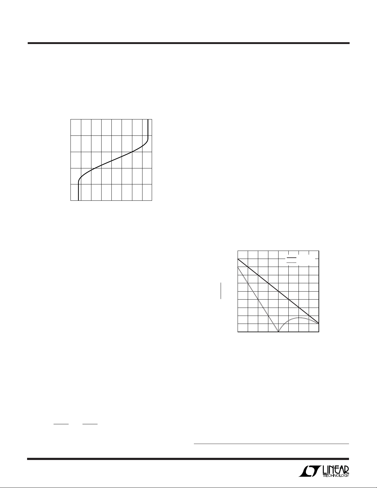
A graph for the voltage applied to the PLLFLTR pin vs
frequency is given in Figure␣ 2. As the operating frequency
is increased the gate charge losses will be higher, reducing
efficiency (see Efficiency Considerations). The maximum
switching frequency is approximately 310kHz.
2.5
2.0
1.5
1.0
FREQSET PIN VOLTAGE (V)
0.5
0
120 170 220 270 320
OPERATING FREQUENCY (kHz)
1929 F02
Figure 2. Operating Frequency vs V
Inductor Value Calculation and Output Ripple Current
The operating frequency and inductor selection are interrelated in that higher operating frequencies allow the use
of smaller inductor and capacitor values. So why would
anyone ever choose to operate at lower frequencies with
larger components? The answer is efficiency. A higher
frequency generally results in lower efficiency because of
MOSFET gate charge and transition losses. In addition to
this basic tradeoff, the effect of inductor value on ripple
current and low current operation must also be considered. The PolyPhase approach reduces both input and
output ripple currents while optimizing individual output
stages to run at a lower fundamental frequency, enhancing
efficiency.
The inductor value has a direct effect on ripple current. The
inductor ripple current ∆IL per individual section, N,
decreases with higher inductance or frequency and increases with higher VIN or V
V
∆I
OUT OUT
=−
L
fL
V
1
V
IN
:
OUT
where f is the individual output stage operating frequency.
PLLFLTR
In a 2-phase converter, the net ripple current seen by the
output capacitor is much smaller than the individual
inductor ripple currents due to the ripple cancellation. The
details on how to calculate the net output ripple current
can be found in Application Note 77.
Figure 3 shows the net ripple current seen by the output
capacitors for the 1- and 2-phase configurations. The
output ripple current is plotted for a fixed output voltage as
the duty factor is varied between 10% and 90% on the
x-axis. The output ripple current is normalized against the
inductor ripple current at zero duty factor. The graph can
be used in place of tedious calculations, simplifying the
design process.
Accepting larger values of ∆IL allows the use of low
inductances, but can result in higher output voltage ripple.
A reasonable starting point for setting ripple current is ∆I
= 0.4(I
)/2, where I
OUT
is the total load current. Remem-
OUT
L
ber, the maximum ∆IL occurs at the maximum input
voltage. The individual inductor ripple currents are determined by the inductor, input and output voltages.
1.0
OUT/VIN
)]
1-PHASE
2-PHASE
)
1929 F03
0.9
0.8
0.7
0.6
/fL
0.5
O
O(P-P)
V
∆I
0.4
0.3
0.2
0.1
0
0.1 0.2 0.3 0.4
Figure 3. Normalized Output Ripple Current vs
Duty Factor [I
DUTY FACTOR (V
≈ 0.3 (∆I
RMS
0.5 0.6 0.7 0.8 0.9
O(P–P)
Inductor Core Selection
Once the values for L1 and L2 are known, the type of
inductor must be selected. High efficiency converters
generally cannot afford the core loss found in low cost
powdered iron cores, forcing the use of more expensive
ferrite, molypermalloy, or Kool Mµ® cores. Actual core
loss is independent of core size for a fixed inductor value,
Kool Mµ is a registered trademark of Magnetics, Inc.
8
 Loading...