

FEATURES
■
High Efficiency: Up to 95%
■
Low Quiescent Current: Only 15µA with No Load
■
550kHz Constant Frequency Operation
■
2.65V to 10V Input Voltage Range
■
V
from 0.8V to VIN, I
OUT
■
True PLL Frequency Locking from 350kHz to 750kHz
■
Power Good Output Voltage Monitor
■
Low Dropout Operation: 100% Duty Cycle
■
Burst Mode® or Pulse Skipping Operation
■
Current Mode Operation for Excellent Line and Load
OUT
to 1.2A
Transient Response
■
Shutdown Mode Draws <1µA Supply Current
■
±2% Output Voltage Accuracy
■
Overcurrent and Overtemperature Protected
■
Available in 16-Lead SSOP Package
U
APPLICATIO S
■
Cellular Telephones
■
Portable Computers
■
Wireless Modems
LTC1879
1.2A Synchronous
Step-Down Regulator with
15µA Quiescent Current
U
DESCRIPTIO
The LTC®1879 is a high efficiency monolithic synchronous buck regulator using a constant frequency, current
mode architecture. Operating supply current is only 15µA
with no load and drops to <1µA in shutdown. The input
supply voltage range of 2.65V to 10V makes the LTC1879
ideally suited for both single and dual Li-Ion battery-powered applications. 100% duty cycle provides low dropout
operation, extending battery life in portable systems.
The switching frequency is internally set to 550kHz, allowing the use of small surface mount inductors and capacitors. For noise sensitive applications, the LTC1879 can be
externally synchronized from 350kHz to 750kHz. Burst
Mode operation is inhibited during synchronization or
when the SYNC/MODE pin is pulled low.
The internal synchronous rectifier switch increases efficiency and eliminates the need for an external Schottky
diode. Low output voltages are easily supported with a
0.8V feedback reference voltage. The LTC1879 is available
in a 16-lead SSOP package.
, LTC and LT are registered trademarks of Linear Technology Corporation.
Burst Mode is a registered trademark of Linear Technology Corporation.
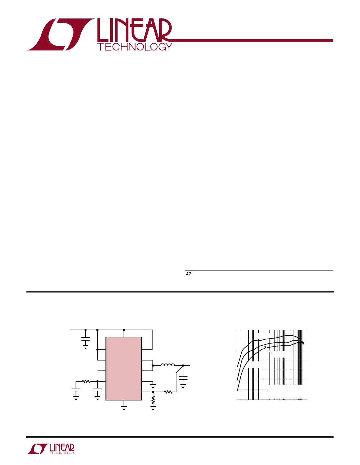
TYPICAL APPLICATIO
High Efficiency Step-Down Converter
V
IN
2.65V TO 10V
C
C
L1: TOKO A921CY6R2M
*V
C
IN
10µF
150k
47pF
: TAIYO YUDEN CERAMIC LMK325BJ106MN
IN
: TDK CERAMIC C4532X5ROJ476M
OUT
OUT
220pF
CONNECTED TO VIN (MINUS SWITCH AND L1 VOLTAGE DROP) FOR 2.65V < VIN < 3.1V
2
15
14
4
RUN/SS
SYNC/MODE
PGOOD
I
TH
U
13
SV
IN
LTC1879
SGND
1
PV
SWP
SWN
PGND
V
Efficiency vs Output Load Current
100
90
8, 9
IN
5, 12
6, 11
7, 10
3
FB
28.0k
1879 TA01a
L1
6.2µH
80.6k
V
3.1V
C
OUT
47µF
OUT
*
80
70
60
EFFICIENCY (%)
50
40
30
0.1 10 100
VIN = 3.6V
VIN = 7.2V
VIN = 10V
Burst Mode OPERATION
= 3.1V
V
OUT
L = 6.2µH
1 1000
OUPUT CURRENT (mA)
1879 TA01b
1879f
1
LTC1879
WW
W
ABSOLUTE MAXIMUM RATINGS
U
U
W
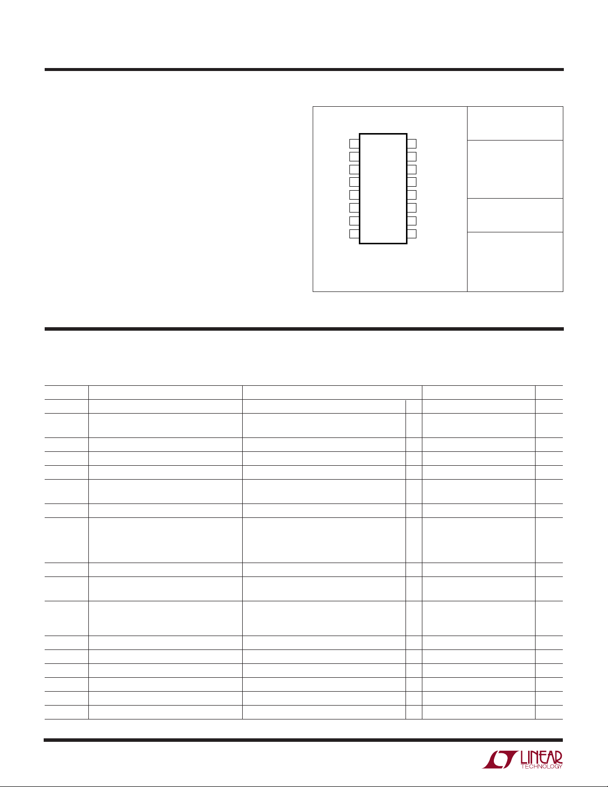
PACKAGE/ORDER INFORMATION
U
(Note 1)
Input Supply Voltage ................................ –0.3V to 11V
ITH, PLL_LPF Voltages............................. –0.3V to 2.7V
RUN/SS, VFB Voltages ............................... – 0.3V to V
SYNC/MODE Voltage ................................. –0.3V to V
(V
– V
PVIN
V
Voltage............................................ –0.3V to 11V
SWN
) Voltage............................. –0.3V to 11V
SWP
IN
IN
P-Channel Switch Source Current (DC) .................... 2A
N-Channel Switch Sink Current (DC) ........................ 2A
Peak Switching Sink and Source Current ................. 3A
Operating Ambient Temperature Range
(Note 2) ............................................. –40°C to 85°C
Junction Temperature (Notes 3, 6) ...................... 125°C
TOP VIEW
1
SGND
2
RUN/SS
3
V
FB
4
I
TH
5
SWP1
6
SWN1
7
PGND1
8
PV
IN1
GN PACKAGE
16-LEAD PLASTIC SSOP
T
= 125°C, θJA = 140°C/ W, θJC = 40°C/W
JMAX
16
PLL_LPF
15
SYNC/MODE
14
PGOOD
13
SV
12
SWP2
11
SWN2
10
PGND2
9
PV
IN
IN2
ORDER PART
NUMBER
LTC1879EGN
GN PART
MARKING
1879
Storage Temperature Range ................ –65°C to 150°C
Lead Temperature (Soldering, 10 sec)................. 300°C
Consult LTC Marketing for parts specified with wider operating temperature ranges.
ELECTRICAL CHARACTERISTICS
The ● denotes specifications which apply over the full operating temperature range, otherwise specifications are TA = 25°C.
VIN = 5V unless otherwise noted.
SYMBOL PARAMETER CONDITIONS MIN TYP MAX UNITS
I
VFB
V
FB
∆V
OVL
∆V
UVL
∆VFB/V
V
LOADREG
V
IN
I
Q
f
SYNC
f
OSC
I
PLLLPF
R
PFET
R
NFET
I
PK
I
LSW
V
SYNC/MODE
I
SYNC/MODE
Feedback Current (Note 4) ● 860 nA
Regulated Output Voltage (Note 4) 0°C ≤ TA ≤ 85°C 0.784 0.80 0.816 V
(Note 4) –40°C ≤ T
Overvoltage Trip Limit with Respect to VFB∆V
Undervoltage Trip Limit with Respect to VFB∆V
Reference Voltage Line Regulation VIN = 2.65V to 10V (Note 4) 0.05 0.25 %/V
FB
Output Voltage Load Regulation Measured in Servo Loop, V
Input Voltage Range ● 2.65 10 V
Input DC Bias Current (Note 5)
Pulse Skipping Mode 2.65V < V
Burst Mode Operation V
Shutdown V
SYNC Capture Range 350 750 kHz
Oscillator Frequency VFB ≥ 0.7V 495 550 605 kHz
Phase Detector Output Current
Sinking Capability f
Sourcing Capability f
R
of P-Channel FET ISW = 100mA, VIN = 5V 0.35 0.45 Ω
DS(ON)
R
of N-Channel FET ISW = –100mA, VIN = 5V 0.37 0.5 Ω
DS(ON)
Peak Inductor Current VFB = 0.7V, Duty Cycle < 35%, V
SW Leakage V
SYNC/MODE Threshold ● 0.2 1.0 1.5 V
SYNC/MODE Leakage Current ±0.01 ±1 µA
= V
OVL
OVL
= VFB – V
UVL
Measured in Servo Loop, V
IN
SYNC/MODE
= 0V, VIN = 10V 0 1 µA
RUN
VFB = 0V 80 kHz
< f
PLLIN
OSC
> f
PPLIN
SOC
= 0V, V
RUN
≤ 85°C ● 0.740 0.80 0.840 V
A
– V
FB
UVL
< 10V, V
= VIN, I
OUT
= 0V or 10V, V
SW
= 0.9V to 1.2V ● 0.1 0.6 %
ITH
= 1.6V to 1.2V ● –0.1 –0.6 %
ITH
SYNC/MODE
= 0V, I
= 0A 15 22 µA
OUT
= 5V 1.8 2.2 2.7 A
IN
= 10V ±0.01 ±2.5 µA
IN
● 20 60 110 mV
● 20 60 110 mV
= 0A 270 365 µA
● 3 10 20 µA
● –3 –10 –20 µA
2
1879f
LTC1879
INPUT VOLTAGE (V)
2
0
R
DS(ON)
(Ω)
0.1
0.2
0.3
0.4
46
8
10
1879 G06
0.5
0.6
35
7
9
SYNCHRONOUS
SWITCH
MAIN
SWITCH
ELECTRICAL CHARACTERISTICS
The ● denotes specifications which apply over the full operating temperature range, otherwise specifications are TA = 25°C.
VIN = 5V unless otherwise noted.
SYMBOL PARAMETER CONDITIONS MIN TYP MAX UNITS
V
RUN
I
RUN
Note 1: Absolute Maximum Ratings are those values beyond which the life
of a device may be impaired.
Note 2: The LTC1879E is guaranteed to meet specified performance from
0°C to 70°C. Specifications over the –40°C to 85°C operating ambient
temperature range are assured by design, characterization and correlation
with statistical process controls.
Note 3: T
dissipation P
LTC1879: TJ = TA + (PD × 140°C/W)
RUN Threshold V
RUN Input Current V
is calculated from the ambient temperature T
J
according to the following formula:
D
Ramping Up ● 0.2 0.7 1.5 V
RUN
= 0V ±0.01 ±1 µA
RUN
Note 4: The LTC1879 is tested in a feedback loop which servos V
balance point for the error amplifier (V
= 1.2V)
ITH
Note 5: Dynamic supply current is higher due to the gate charge being
delivered at the switching frequency.
Note 6: This IC includes overtemperature protection that is intended to
protect the device during momentary overload conditions. Junction
and power
A
temperature will exceed 125°C when overtemperature protection is active.
Continuous operation above the specified maximum operating junction
temperature may impair device reliability.
FB
to the
UW
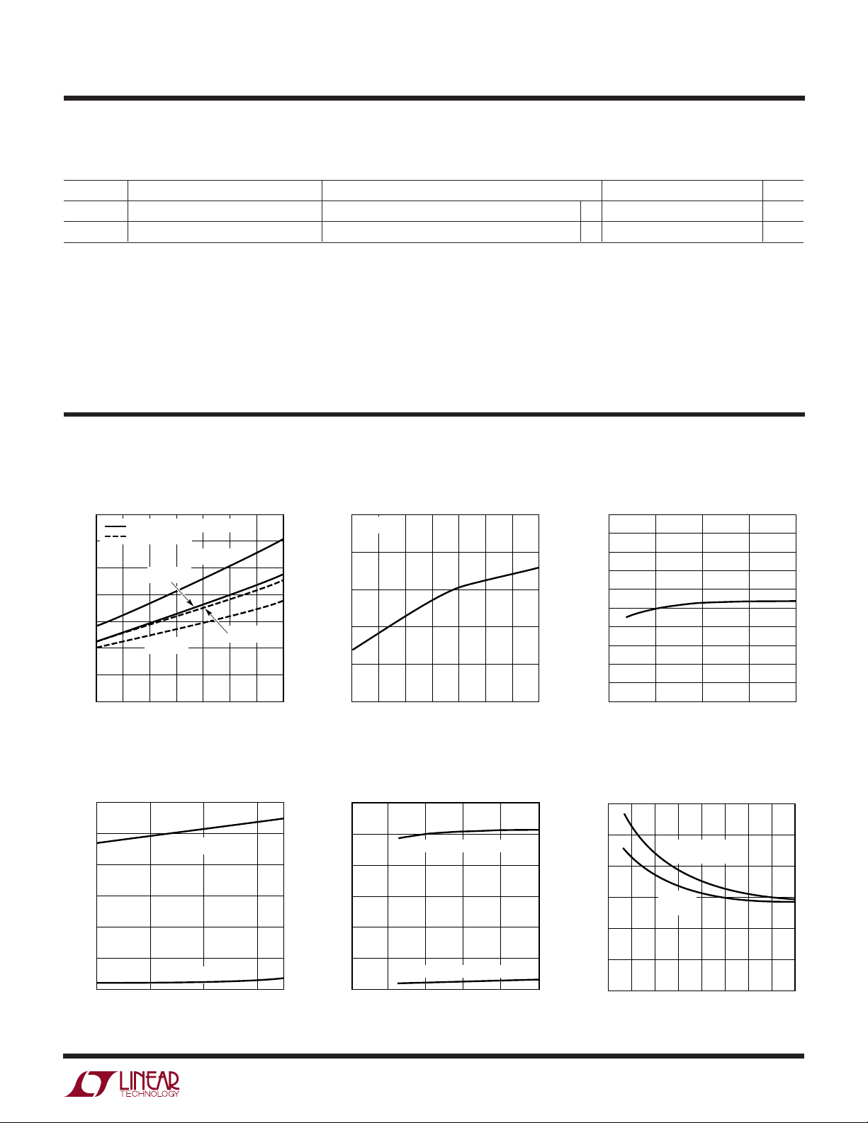
TYPICAL PERFOR A CE CHARACTERISTICS
R
vs Temperature
DS(ON)
0.7
0.6
0.5
0.4
(Ω)
0.3
DS(ON)
R
0.2
0.1
0
SYNCHRONOUS SWITCH
MAIN SWITCH
VIN = 5V
VIN = 10V
VIN = 10V
–50 –25 0 25 50 75 100 125
TEMPERATURE (°C)
VIN = 5V
DC Supply Current
vs Temperature
300
VIN = 5V
250
200
150
PULSE SKIPPING MODE
1879 G01
Oscillator Frequency
vs Temperature
595
VIN = 5V
575
555
535
FREQUENCY (kHz)
515
495
–50 –25 0 25 50 75 100 125
TEMPERATURE (°C)
DC Supply Current
vs Input Voltage
300
250
200
150
PULSE SKIPPING MODE
1879 G02
Oscillator Frequency
vs Supply Voltage
600
590
580
570
560
550
540
530
520
OSCILLATOR FREQUENCY (kHz)
510
500
2 4 6810
R
SUPPLY VOLTAGE (V)
vs Input Voltage
DS(ON)
1879 G03
SUPPLY CURRENT (µA)
100
50
0
–50
0 50 100 125
TEMPERATURE (°C)
Burst Mode OPERATON
1879 G04
100
DC SUPPLY CURRENT (µA)
50
0
0
Burst Mode OPERATION
2468
INPUT VOLTAGE (V)
1879 G05
10
1879f
3
LTC1879
UW
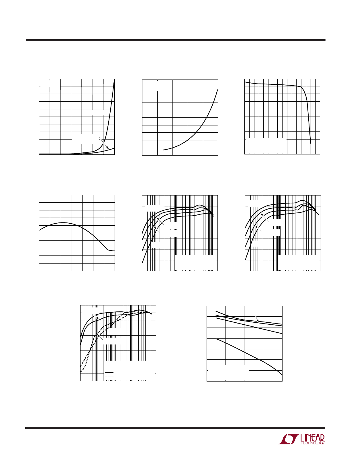
TYPICAL PERFOR A CE CHARACTERISTICS
Switch Leakage vs Temperature
20
VIN = 10V
18
16
14
12
10
8
6
SWITCH LEAKAGE (µA)
4
2
0
–50
0
–25
TEMPERATURE (°C)
MAIN SWITCH
SYNCHRONOUS
SWITCH
50
25
75
Reference Voltage
vs Temperature
804
VIN = 6V
803
802
801
800
799
798
797
REFERENCE VOLTAGE (mV)
796
795
794
–50 –25 0 25 50 75 100 125
TEMPERATURE (°C)
100
1879 G07
1879 G10
125
Switch Leakage vs Input Voltage Output Voltage vs Load Current
50
RUN = 0V
45
= 25°C
T
A
40
35
30
25
20
15
SWITCH LEAKAGE (nA)
10
5
0
2
0
MAIN SWITCH
SYNCHRONOUS SWITCH
4
INPUT VOLTAGE (V)
Efficiency vs Output Current
100
90
VIN = 3.6V
80
70
60
EFFICIENCY (%)
50
40
30
0.1 10 100
VIN = 5V
VIN = 7.2V
VIN = 10V
V
OUT
L = 6.2µH
Burst Mode OPERATION
1 1000
OUTPUT CURRENT (mA)
6
= 1.8V
8
10
1879 G08
1879 G11
2.51
2.50
2.49
2.48
2.47
2.46
2.45
2.44
OUTPUT VOLTAGE (V)
2.43
PULSE SKIPPING MODE
V
= 5V
2.42
IN
L = 6.2µH
2.41
0
200 600
400
800
LOAD CURRENT (mA)
Efficiency vs Output Current
100
VIN = 3.6V
90
80
70
60
EFFICIENCY (%)
50
40
30
0.1 10 100
VIN = 5V
VIN = 7.2V
VIN = 10V
V
OUT
L = 6.2µH
Burst Mode OPERATION
1 1000
OUTPUT CURRENT (mA)
1000
= 2.5V
1200
1400
1600
1879 G09
1879 G12
4
Efficiency vs Output Current
100
VIN = 7.2V
90
80
70
60
50
40
EFFICIENCY (%)
30
20
10
0
0.1 10 100
VIN = 4.2V
VIN = 4.2V
VIN = 7.2V
V
OUT
L = 6.2µH
Burst Mode OPERATION
PULSE SKIPPING MODE
1 1000
OUTPUT CURRENT (mA)
= 3.1V
1879 G13
Efficiency vs Input Voltage
100
90
80
70
60
EFFICIENCY (%)
50
V
40
L = 6.2µH
Burst Mode OPERATION
30
2
100mA 10mA
1mA
= 2.5V
OUT
46 10
INPUT VOLTAGE (V)
0.1mA
8
1879 G14
1879f
UW
TYPICAL PERFOR A CE CHARACTERISTICS
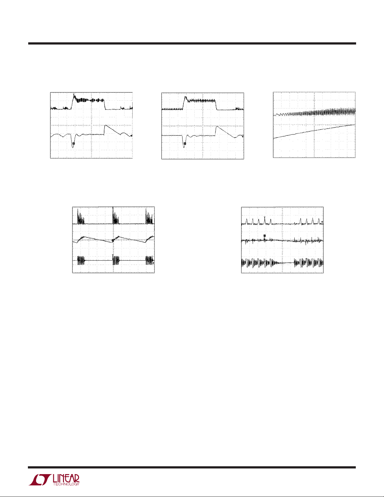
Load Step
Load Step (Burst Mode Operation)
I
L
1A/DIV
(Pulse Skipping Mode)
I
L
1A/DIV
I
VIN
500mA/DIV
LTC1879
Soft-Start with Shorted Output
V
OUT
100mV/DIV
VIN = 5V CIN = 20µF
= 2.5V C
V
OUT
L = 4.7µHI
200mA/DIV
V
OUT
50mV/DIV
SW
5V/DIV
50µs/DIV
= 47µF
OUT
= 50mA to 1200mA
LOAD
I
L
VIN = 5V CIN = 20µF
= 2.5V C
V
OUT
L = 4.7µHI
OUT
LOAD
25µs/DIV
= 47µF
= 15mA
1879 G15
V
OUT
100mV/DIV
1879 G18
VIN = 5V CIN = 20µF
= 2.5V C
V
OUT
L = 4.7µHI
50µs/DIV
= 47µF
OUT
= 50mA to 1200mA
LOAD
200mA/DIV
V
OUT
20mV/DIV
SW
5V/DIV
RUN/SS
1V/DIV
1879 G16
Pulse Skipping Mode OperationBurst Mode Operation
I
L
VIN = 5V CIN = 20µF
V
= 2.5V C
OUT
L = 4.7µHI
VIN = 5V CIN = 20µF
= 0V C
V
OUT
L = 4.7µHI
2.5µs/DIV
= 47µF
OUT
= 15mA
LOAD
OUT
LOAD
5ms/DIV
= 47µF
= 0A
1879 G17
1879 G19
1879f
5

LTC1879
U
UU
PI FU CTIO S
SGND (Pin 1): Signal Ground Pin.
RUN/SS (Pin 2): Combination of Soft-Start and Run
Control Inputs. Forcing this pin below 0.7V shuts down the
device. In shutdown all functions are disabled and device
draws zero supply current. For the proper operation of the
part, force this pin above 2.5V. Do not leave this pin
floating. Soft-start can be accomplished by raising the
voltage on this pin gradually with an RC circuit.
VFB (Pin 3): Feedback Pin. Receives the feedback voltage
from an external resistor divider across the output.
ITH (Pin 4): Error Amplifier Compensation Point. The
current output increases with this control voltage. Nominal voltage range for this pin is 0.5V to 1.8V.
SWP1, SWP2 (Pins 5, 12): Upper Switch Nodes. These
pins connect to the drains of the internal main PMOS
switches and should always be connected together
externally.
SWN1, SWN2 (Pins 6, 11): Lower Switch Nodes. These
pins connect to the drains of the internal synchronous
NMOS switches and should always be connected together
externally.
PV
, PV
IN1
Internal Drivers and Switches. These pins should always
be tied together.
SVIN (Pin 13): Signal Power Supply Pin.
PGOOD (Pin 14): Power Good Indicator Pin. Power good
is an open-drain logic output. The PGOOD pin is pulled to
ground when the voltage on the VFB pin is not within
±7.5% of its nominally regulated potential. This pin requires a pull-up resistor for power good indication. Power
good indication works in all modes of operation.
SYNC/MODE (Pin 15): External Clock Synchronization
and Mode Select Input. To synchronize, apply an external
clock with a frequency between 350kHz and 750kHz. To
select Burst Mode operation, tie pin to SVIN. Grounding
this pin selects pulse skipping mode. Do not leave this pin
floating.
PLL_LPF (Pin 16): Output of the Phase Detector and
Control Input of Oscillator. Connect a series RC lowpass
network from this pin to ground if externally synchronized.
If unused, this pin may be left open.
(Pins 8, 9): Power Supply Pins for the
IN2
PGND1, PGND2 (Pins 7, 10): Power Ground Pins. Ground
pins for the internal drivers and switches. These pins
should always be tied together.
6
1879f

BLOCK DIAGRA
LTC1879
W
PGND
+
RCMP
SHUTDOWN
7, 10
–
1879 BD
PGOOD
14
SGND
1
8, 9
IN
13
SV
IN
PV
TOP
2.9Ω
SWP
MOSFET
5, 12
6, 11
SWN
BOTTOM
MOSFET
+
COMP
I
0.8V
–
SLEEP
EN
–
BURST
+
Q
S
AND
LOGIC
SWITCHING
Q
R
RS LATCH
ANTI-
SHOOT-
THROUGH
CIRCUIT
BLANKING
THERMAL
SHUTDOWN
OSC
COMP
SLOPE
VCO
OSC
AND
Y = “0” ONLY WHEN X IS A CONSTANT “1”
Y
X
BURST DEFEAT
PLL_LPF
16
SYNC/MODE
15
–
0.6V
–
FREQ
+
FB
V
SHIFT
3
0.45V
4
TH
I
OV
+
IN
SLEEP
SV
UVDET
+
0.74V
+
0.8V
OVDET
EA
–
+
–
0.86V
IN
SV
0.8V REF
RUN/SS
2
–
SOFT-START
1879f
7

LTC1879
OPERATIO
U
(Refer to Block Diagram)
Main Control Loop
The LTC1879 uses a constant frequency, current mode
step-down architecture. Both the top MOSFET and synchronous bottom MOSFET switches are internal. During
normal operation, the internal top power MOSFET is
turned on each cycle when the oscillator sets the RS latch,
and turned off when the current comparator, I
the RS latch. The peak inductor current at which I
COMP
, resets
COMP
turns the top MOSFET off is controlled by the voltage on
the ITH pin, which is the output of error amplifier EA. When
the load current increases, it causes a slight decrease in
the feedback voltage, VFB, relative to the 0.8V internal
reference, which, in turn, causes the I
voltage to in-
TH
crease until the average inductor current matches the new
load current. While the top MOSFET is off, the bottom
MOSFET is turned on until either the inductor current
starts to reverse direction or the next clock cycle begins.
Comparator OVDET guards against transient overshoots
>7.5% by turning the main switch off and keeping it off
until the fault is removed.
Burst Mode Operation
The LTC1879 is capable of Burst Mode operation in which
the internal power MOSFETs operate intermittently based
on load demand. To enable Burst Mode operation, simply
tie the SYNC/MODE pin to SV
(V
SYNC/MODE
> 1.5V). To disable Burst Mode operation
or connect it to a logic high
IN
and enable PWM pulse skipping mode, connect the SYNC/
MODE pin to SGND. In this mode, the efficiency is lower at
light loads but becomes comparable to Burst Mode operation when the output load exceeds 100mA. The advantage
of pulse skipping mode is lower output ripple.
When the converter is in Burst Mode operation, the peak
current of the inductor is set to approximately 400mA,
even though the voltage at the I
value. The voltage at the I
pin drops when the inductor’s
TH
pin indicates a lower
TH
average current is greater than the load requirement. As
the I
voltage drops below approximately 0.45V, the
TH
BURST comparator trips, turning off both power MOSFETs.
The I
pin is then disconnected from the output of the EA
TH
amplifier and held 0.65V above ground.
In sleep mode, both power MOSFETs are held off and the
internal circuitry is partially turned off, reducing the quiescent current to 15µA. The load current is now being
supplied from the output capacitor. When the output
voltage drops, the I
pin reconnects to the output of the
TH
EA amplifier and the top MOSFET is again turned on and
this process repeats.
Soft-Start/Run Function
The RUN/SS pin provides a soft-start function and a
means to shut down the LTC1879. Soft-start reduces the
input current surge by gradually increasing the regulator’s
maximum output current. This pin can also be used for
power supply sequencing.
Pulling the RUN/SS pin below 0.7V shuts down the
LTC1879, which then draws <1µA current from the sup-
ply. This pin can be driven directly from logic circuits as
shown in Figure 1. It is recommended that this pin is driven
to VIN during normal operation. Note that there is no
current flowing out of this pin. Soft-start action is accomplished by connecting an external RC network to the RUN/
SS pin as shown in Figure 1. The LTC1879 actively pulls
the RUN/SS pin to ground under low input supply voltage
conditions.
V
IN
3.3V OR 5V
Figure 1. RUN/SS Pin Interfacing
D1*
0.32V
*ZETEX BAT54
R
SS
RUN/SS
C
SS
1879 F01
8
1879f

OPERATIO
LTC1879
U
(Refer to Block Diagram)
Power Good Indicator
The power good function monitors the output voltage in all
modes of operation. Its open-drain output is pulled low
when the output voltage is not within ±7.5% of its nominally regulated voltage. The feedback voltage is filtered
before it is fed to a power good window comparator in
order to prevent false tripping of the power good signal
during fast transients. The window comparator monitors
the output voltage even in Burst Mode operation. In
shutdown mode, open drain is actively pulled low to
indicate that the output voltage is invalid.
Short-Circuit Protection
When the output is shorted to ground, the frequency of
the oscillator is reduced to about 80kHz, 1/7 the nominal
frequency. This frequency foldback ensures that the inductor current has more time to decay, thereby preventing
runaway. The oscillator’s frequency will progressively
increase to 550kHz (or to the synchronized frequency)
when V
rises above 0.3V.
FB
Frequency Synchronization
The LTC1879 can be synchronized to an external clock
source connected to the SYNC/MODE pin. The turn-on of
the top MOSFET is synchronized to the rising edge of the
external clock.
When the LTC1879 is clocked by an external source, Burst
Mode operation is disabled. In this synchronized mode,
when the output load current is very low, current comparator, I
, may remain tripped for several cycles and force
COMP
the main switch to stay off for the same number of cycles.
Increasing the output load slightly allows constant frequency PWM operation to resume.
Frequency synchronization is inhibited when the feedback
voltage V
is below 0.6V. This prevents the external clock
FB
from interfering with the frequency foldback for shortcircuit protection.
Low Dropout Operation
When the input supply voltage decreases toward the
output voltage in a buck regulator, the duty cycle increases toward the maximum on-time. Further reduction
of the supply voltage forces the main switch to remain on
for more than one cycle until it reaches 100% duty cycle.
The output voltage will then be determined by the input
voltage minus the voltage drop across the top MOSFET
and the inductor.
Low Supply Operation
The LTC1879 is designed to operate down to an input
supply voltage of 2.65V although the maximum allowable
output current is reduced at this low voltage. Figure 2
shows the reduction in the maximum output current as a
function of input voltage.
Another important detail to remember is that at low input
supply voltages, the R
of the P-channel switch
DS(ON)
increases. Therefore, the user should calculate the power
dissipation when the LTC1879 is used at 100% duty cycle
with low supply voltage (see Thermal Considerations in
the Applications Information section).
1800
1600
V
= 2.5V
1400
1200
1000
800
600
MAXIMUM OUTPUT CURRENT (mA)
400
2
Figure 2. Maximum Output Current vs Input Voltage
OUT
V
= 1.8V
OUT
V
= 3.1V
OUT
436
57 10
INPUT VOLTAGE (V)
8
9
1879 F02
1879f
9

LTC1879
U
OPERATIO
Slope Compensation and Inductor Peak Current
Slope compensation is required in order to prevent subharmonic oscillation at high duty cycles. It is accomplished by internally adding a compensating ramp to the
inductor current signal at duty cycles in excess of 40%. As
a result, the maximum inductor peak current is reduced for
duty cycles >40%. This is shown in the decrease of the
inductor peak current as a function of duty cycle graph in
Figure 3.
WUUU
APPLICATIO S I FOR ATIO
2400
VIN = 5V
2200
2000
1800
1600
1400
1200
MAXIMUM INDUCTOR PEAK CURRENT (mA)
1000
0
20 40 60 80
DUTY CYCLE (%)
Figure 3. Maximum Inductor Peak Current vs Duty Cycle
100
1879 F03
The basic LTC1879 application circuit is shown on the first
page of this data sheet. External component selection is
driven by the load requirement and begins with the selection of L followed by C
IN
and C
OUT
.
Inductor Value Calculation
The inductor selection will depend on the operating frequency of the LTC1879. The internal nominal frequency is
550kHz, but can be externally synchronized from 350kHz
to 750kHz.
The operating frequency and inductor selection are interrelated in that higher operating frequencies allow the use
of smaller inductor and capacitor values. However, operating at a higher frequency results in lower efficiency
because of increased switching losses.
The inductor value has a direct effect on ripple current. The
ripple current ∆IL decreases with higher inductance or
frequency and increases with higher input voltages.
I
∆=
1
L OUT
fL
()()
V
1–
V
OUT
V
IN
(1)
Accepting larger values of ∆IL allows the use of smaller
inductors, but results in higher output voltage ripple.
A reasonable starting point for setting ripple current is
∆IL = 0.3(I
MAX
).
The inductor value also has an effect on Burst Mode
operation. The transition to low current operation begins
when the inductor current peaks fall to approximately
500mA. Lower inductor values (higher ∆IL) will cause this
to occur at lower load currents, which can cause a dip in
efficiency in the upper range of low current operation. In
Burst Mode operation, lower inductance values will cause
the burst frequency to increase.
Inductor Selection
The inductor should have a saturation current rating
greater than the peak inductor current set by the current
comparator of LTC1879. Also, consideration should be
given to the resistance of the inductor. Inductor conduction losses are directly proportional to the DC resistance
of the inductor.
Manufacturers sometimes provide maximum current ratings based on the allowable losses in the
inductor.
Suitable inductors are available from Coilcraft, Cooper,
Dale, Sumida, Toko, Murata, Panasonic and other manufacturers.
10
1879f

WUUU
APPLICATIO S I FOR ATIO
C
and C
IN
In continuous mode, the source current of the top MOSFET
is a trapezoidal waveform of duty cycle V
prevent large voltage transients, a low ESR input capacitor
sized for the maximum RMS current must be used. The
maximum RMS input capacitor current is given by:
II
RMS CIN OMAX
This formula has a maximum at V
I
= I
RMS
monly used for design because even significant deviations do not offer much relief. Note that the capacitor
manufacturer’s ripple current ratings are often based on
2000 hours of life. This makes it advisable to further
derate the capacitor, or choose a capacitor rated at a
higher temperature than required. Several capacitors may
also be paralleled to meet size or height requirements in
the design. Always consult the manufacturer if there are
any questions.
Depending on how the LTC1879 circuit is powered up,
you may need to check for input voltage transients. Input
voltage transients may be caused by input voltage steps
or by connecting the circuit to an already powered up
source such as a wall adapter. The sudden application of
input voltage will cause a large surge of current in the
input leads that will store energy in the parasitic inductance of the leads. This energy will cause the input voltage
to swing above the DC level of the input power source and
it may exceed the maximum voltage rating of the input
capacitor and LTC1879.
The easiest way to suppress input voltage transients is to
add a small aluminum electrolytic capacitor in parallel
with the low ESR input capacitor. The selected capacitor
needs to have the right amount of ESR in order to critically
dampen the resonant circuit formed by the input lead
inductance and the input capacitor. The typical values of
ESR will fall in the range of 0.5Ω to 2Ω and capacitance
will fall in the range of 5µF to 50µF.
Selection
OUT
OUT/VIN
/
IN
12
= 2V
OUT
, where
VVV
(– )
[]
≅
()
/2. This simple worst-case condition is com-
OUT
OUT IN OUT
V
IN
. To
LTC1879
The selection of C
series resistance (ESR). Typically, once the ESR requirement is satisfied, the capacitance is adequate for filtering.
The output ripple ∆V
∆≅∆ +
V I ESR
OUT L
where f = operating frequency, C
and ∆IL = ripple current in the inductor. The output ripple
is highest at maximum input voltage since ∆IL increases
with input voltage. For the LTC1879, the general rule for
proper operation is:
ESR
COUT
< 0.125Ω
The choice of using a smaller output capacitance increases the output ripple voltage due to the frequency
dependent term but can be compensated for by using
capacitor(s) of very low ESR to maintain low ripple voltage. The ITH pin compensation components can be optimized to provide stable high performance transient
response regardless of the output capacitor selected.
Manufacturers such as Taiyo Yuden, AVX, Kemet and
Sanyo should be considered for low ESR, high performance capacitors. The POSCAP solid electrolytic chip
capacitor available from Sanyo is an excellent choice for
output bulk capacitors due to its low ESR/size ratio. Once
the ESR requirement for C
current rating generally far exceeds the I
requirement.
Output Voltage Programming
The output voltage is set by a resistor divider according to
the following formula:
VV
=+
08 1
OUT
.
The external resistor divider is connected to the output,
allowing remote voltage sensing as shown in Figure 4.
is driven by the required effective
OUT
is determined by:
OUT
8
R
1
R
2
1
fC
OUT
= output capacitance
OUT
has been met, the RMS
OUT
RIPPLE(P-P)
(2)
1879f
11

LTC1879
WUUU
APPLICATIO S I FOR ATIO
OUT
≤ 10V
R1
R2
1879 F04
0.8V ≤ V
V
FB
LTC1879
SGND
Figure 4. Setting the LTC1879 Output Voltage
Phase-Locked Loop and Frequency Synchronization
The LTC1879 has an internal voltage-controlled oscillator
and phase detector comprising a phase-locked loop. This
allows the MOSFET turn-on to be locked to the rising edge
of an external frequency source. The frequency range of
the voltage-controlled oscillator is 350kHz to 750kHz. The
phase detector used is an edge sensitive digital type that
provides zero degrees phase shift between the external
and internal oscillators. This type of phase detector will not
lock up on input frequencies close to the harmonics of the
VCO center frequency. The PLL hold-in range ∆fH is equal
to the capture range, ∆fH = ∆fC = ±200kHz.
The output of the phase detector is a pair of complementary current sources charging or discharging the external
filter network on the PLL_LPF pin. The relationship between the voltage on the PLL_LPF pin and operating
frequency is shown in Figure 5. A simplified block diagram
is shown in Figure 6.
1000
900
800
700
600
500
400
300
OSC FREQUECNY (kHz)
200
100
0
0
Figure 5. Relationship Between Oscillator Frequency
and Voltage at PLL_LPF Pin
0.5 1 1.5 2
V
(V)
PLLLPF
1879 F05
R
LP
2.4V
SYNC/
MODE
DIGITAL
PHASE/
FREQUENCY
DETECTOR
Figure 6. Phase-Locked Loop Block Diagram
If the external frequency (V
SYNC/MODE
PLL_LPF
VCO
) is greater than
1879 F06
C
LP
550kHz, the center frequency, current is sourced continuously, pulling up the PLL_LPF pin. When the external
frequency is less than 550kHz, current is sunk continuously, pulling down the PLL_LPF pin. If the external and
internal frequencies are the same but exhibit a phase
difference, the current sources turn on for an amount of
time corresponding to the phase difference. Thus the
voltage on the PLL_LPF pin is adjusted until the phase and
frequency of the external and internal oscillators are
identical. At this stable operating point the phase comparator output is open and the filter capacitor CLP holds the
voltage.
The loop filter components CLP and R
smooth out the
LP
current pulses from the phase detector and provide a
stable input to the voltage controlled oscillator. The filter
components CLP and RLP determine how fast the loop
acquires lock. Typically R
= 10k and C
LP
is 2200pF to
LP
0.01µF. When not synchronized to an external clock, the
internal connection to the VCO is disconnected. This
disallows setting the internal oscillation frequency by a DC
voltage on the V
PLLLPF
pin.
Efficiency Considerations
The efficiency of a switching regulator is equal to the
output power divided by the input power times 100%. It is
often useful to analyze individual losses to determine what
is limiting the efficiency and which change would produce
the most improvement. Efficiency can be expressed as:
Efficiency = 100% – (ρ1 + ρ2 + ρ3 + ...)
1879f
12

WUUU
APPLICATIO S I FOR ATIO
LTC1879
Where ρ1, ρ2, etc. are the individual losses as a percent-
age of input power.
Although all dissipative elements in the circuit produce
losses, two main sources usually account for most of the
losses in LTC1879 circuits: supply quiescent currents and
I2R losses. The supply quiescent current loss dominates
the efficiency loss at very low load current whereas the I2R
loss dominates the efficiency loss at medium to high load
currents. In a typical efficiency plot, the efficiency curve at
very low load currents can be misleading since the actual
power lost is of no consequence as illustrated in Figure 7.
1.
The supply quiescent current is due to two components: the DC bias current as given in the Electrical
Characteristics and the internal main switch and synchronous switch gate charge currents. The gate charge
current results from switching the gate capacitance of
the internal power MOSFET switches. Each time the
gate is switched from high to low to high again, a
packet of charge dQ moves from PVIN to ground. The
resulting dQ/dt is the current out of PV
that is typically
IN
larger than the DC bias current. In continuous mode,
I
GATECHG
= f(QT + QB) where QT and QB are the gate
charges of the internal top and bottom switches. Both
the DC bias and gate charge losses are proportional to
supply voltage and thus their effects will be more
pronounced at higher supply voltages.
1
VIN = 6V
= 3.3V
V
OUT
L = 6.8µH
Burst Mode OPERATION
0.1
0.01
POWER LOST (W)
0.001
2. I2R losses are calculated from the resistances of the
internal switches RSW and external inductor RL. In
continuous mode the average output current flowing
through inductor L is “chopped” between the main
switch and the synchronous switch. Thus, the series
resistance looking into SW pins is a function of both top
and bottom MOSFET R
and the duty cycle (DC) as
DS(ON)
follows:
R
The R
= (R
SW
DS(ON)
DS(ON)TOP
for both the top and bottom MOSFETs can
)(DC) + (R
DS(ON)BOT
)(1 – DC)
be obtained from the Typical Performance Characteristics curves. Thus, to obtain I2R losses, simply add R
SW
to RL and multiply by the square of the average output
current.
Other losses including CIN and C
ESR dissipative
OUT
losses, MOSFET switching losses and inductor core losses
generally account for less than 2% total additional loss.
Thermal Considerations
In most applications, the LTC1879 does not dissipate
much heat due to its high efficiency. But, in applications
where the LTC1879 is running at high ambient temperature with low supply voltage and high duty cycles, such as
in dropout, the heat dissipated may exceed the maximum
junction temperature of the part. If the junction temperature reaches approximately 150°C, both power switches
will be turned off and the SW nodes will become high
impedance.
To avoid the LTC1879 from exceeding the maximum
junction temperature, the user will need to do some
thermal analysis. The goal of the thermal analysis is to
determine whether the power dissipated exceeds the
maximum junction temperature of the part. Normally,
some iterative calculation is required to determine a reasonably accurate value. The temperature rise is given by:
0.0001
0.1
Figure 7. Power Lost vs Load Current
1 10 100 1000
LOAD CURRENT (mA)
1879 F07
TR = P • θ
where P is the power dissipated by the regulator and θ
JA
JA
is the thermal resistance from the junction of the die to the
ambient temperature.
The junction temperature is given by:
TJ = TA + T
R
1879f
13

LTC1879
WUUU
APPLICATIO S I FOR ATIO
where TA is the ambient temperature. Because the power
transistor R
is a function of temperature, it is
DS(ON)
usually necessary to iterate 2 to 3 times through the
equations to achieve a reasonably accurate value for the
junction temperature.
As an example, consider the LTC1879 in dropout at an
input voltage of 5V, a load current of 0.8A and an ambient
temperature of 70°C. From the typical performance graph
of switch resistance, the R
DS(ON)
of the P-channel switch
at 70°C is 0.38Ω. Therefore, power dissipated by the IC is:
P = I2 • R
DS(ON)
= 0.243W
For the SSOP package, the θJA is 140°C/W. Thus the
junction temperature of the regulator is:
TJ = 70°C + (0.243)(140) = 104°C
However, at this temperature, the R
DS(ON)
is actually
0.42Ω.
Therefore:
TJ = 70°C + (0.269)(140) = 108°C
which is below the maximum junction temperature of
125°C.
Note that at higher supply voltages, the junction temperature is lower due to reduced switch resistance (R
DS(ON)
).
Checking Transient Response
The regulator loop response can be checked by looking at
the load transient response. Switching regulators take
several cycles to respond to a step in load current. When
a load step occurs, V
equal to (∆I
resistance of C
discharge C
• ESR), where ESR is the effective series
LOAD
OUT
, generating a feedback error signal. The
OUT
regulator loop then acts to return V
value. During this recovery time, V
immediately shifts by an amount
OUT
. ∆I
also begins to charge or
LOAD
to its steady-state
OUT
can be monitored
OUT
for overshoot or ringing that would indicate a stability
problem. The I
pin can be used for external compensa-
TH
tion as shown in Figure 9. (The capacitor, CC2, is typically
needed for noise decoupling.)
A second, more severe transient is caused by switching in
loads with large (>1µF) supply bypass capacitors. The
discharged bypass capacitors are effectively put in parallel
with C
, causing a rapid drop in V
OUT
. No regulator can
OUT
deliver enough current to prevent this problem if the load
switch resistance is low and it is driven quickly. The only
solution is to limit the rise time of the switch drive so that
the load rise time is limited to approximately (25 • C
LOAD
).
Thus, a 10µF capacitor charging to 3.3V would require a
250µs rise time, limiting the charging current to about
130mA.
14
1879f

WUUU
APPLICATIO S I FOR ATIO
LTC1879
PC Board Layout Checklist
As with all high frequency switchers, when considering
layout, care must be taken in order to achieve optimal
electrical, thermal and noise performance. Figure 8 is a
sample of PC board layout for the design example shown
in Figure 9. A 4-layer PC board is used in this design.
Several guidelines are followed in this layout:
1. In order to minimize switching noise and improve
output load regulation, the PGND pins of the LTC1879
should be connected directly to 1) the negative terminal
of the output decoupling capacitors, 2) the negative
terminal of the input capacitor and 3) vias to the ground
plane immediately adjacent to Pins 1, 7 and 10. The
ground trace on the top layer of the PC board should be
as wide and short as possible to minimize series resistance and inductance.
2. Beware of ground loops in multiple layer PC boards. Try
to maintain one central ground node on the board and
use the input capacitor to avoid excess input ripple for
high output current power supplies. If the ground is to
be used for high DC currents, choose a path away from
the small-signal components.
3. The high di/dt loop from the top terminal of the input
capacitor, through the power MOSFETs and back to the
input capacitor should be kept as tight as possible to
reduce inductive ringing. Excess inductance can cause
increased stress on the power MOSFET and increase
noise on the input. If low ESR ceramic capacitors are
used to reduce input noise, place these capacitors close
to the DUT in order to keep the series inductance to a
minimum.
4. Place the small-signal components away from high
frequency switching nodes. In the layout shown in
Figure 8, all of the small-signal components have been
placed on one side of the IC and all of the power
components have been placed on the other.
5. For optimum load regulation and true sensing, the top
of the output resistor divider should connect independently to the top of the output capacitor (Kelvin connection), staying away from any high dV/dt traces. Place
the divider resistors near the LTC1879 in order to keep
the high impedance FB node short.
VIAS TO GND PLANE
R
C
C
C
C1
C
SS
R
SS
R
FB2
R
FB1
C
IN1
V
IN
C2
DUT
C
IN2
R
C
PL
PL
VIAS TO GND PLANE
R
SVIN
VIA CONNECTION TO R
R
PG
C
OUT
PGND V
Figure 8. Typical Application and Suggested Layout (Topside Only)
FB1
L1
OUT
1879 F08
1879f
15

LTC1879
WUUU
APPLICATIO S I FOR ATIO
Design Example
As a design example, assume the LTC1879 is used in a
dual lithium-ion battery-powered cellular phone application. The VIN will be operating from a maximum of 8.4V
down to about 2.65V. The load current requirement is a
maximum of 0.7A but most of the time it will be on standby
mode, requiring only 2mA. Efficiency at both low and high
load currents is important. Output voltage is 2.5V. With
this information we can calculate L using equation (1),
V
OUT
V
.
•
OUT
1–
= 2.5V, V
L
Substituting V
f = 550kHz in equation (3) gives:
L
1
=
fI
()∆()
L
25
kHz mA
550 210
V
OUT
V
IN
= 8.4V, ∆IL = 210mA and
IN
V
25
.
1
–
84
.
=µ
15 2
V
.
(3)
H=
An 15µH inductor works well for this application. For good
efficiency choose a 1.5A inductor with less than 0.125Ω
series resistance.
C
will require an RMS current rating of at least 0.35A at
IN
temperature and C
0.125Ω. In most applications, the requirements for these
capacitors are fairly similar.
For the feedback resistors, choose R2 = 412k. R1 can then
be calculated from equation (2) to be:
V
R
Figure 9 shows the complete circuit along with its efficiency curve.
OUT
1
–• .,
08
.
will require an ESR of less than
OUT
R k use k
1 2 875 5 887=
=
16
1879f

WUUU
APPLICATIO S I FOR ATIO
C
SVIN
0.1µF
R
C
C2
220pF
100k
C
0.1µF
PG
R
SS
1M
SS
C
C1
47pF
R
C
150k
14
16
2
4
SV
PGOOD
RUN/SS
PLL_LPF
I
TH
IN
LTC1879
1513
SYNC/MODE
PV
PV
PGND
PGND
SWP
SWP
SWN
SWN
V
SGND
LTC1879
R
SVIN
10Ω
8
IN
9
IN
7
10
5
12
6
11
3
FB
1
10µF
R2
412k
C
IN1
L1
15µH
R1
887k
C
OUT
47µF
C
IN2
10µF
1879 F09a
V
IN
2.65V TO 8.4V
GND
V
OUT
2.5V
0.7A
BOLD LINES INDICATE HIGH CURRENT PATHS
, C
: TAIYO YUDEN CERAMIC JMK316BJ106ML
C
IN1
IN2
: TDK CERAMIC C4532X5R0J476M
C
OUT
L1: TOKO A921CY-150M
: 0.7A IS THE MAXIMUM OUTPUT CURRENT
V
OUT
Figure 9a. Dual Lithium-Ion/8V Wall Adapter to 2.5V/0.7A Regulator from Design Example
100
VIN = 3.6V
= 2.5V
V
OUT
L = 15µH
90
80
EFFICIENCY (%)
70
60
0.1 10 100 1000
1
OUTPUT CURRENT (mA)
1879 F09b
Figure 9b. Efficiency vs Output Current for Design Example
1879f
17

LTC1879
TYPICAL APPLICATIO
Dual Li-Ion to 1.8V/1A Regulator Using All Ceramic Capacitors
C
SVIN
0.1µF
R
PG
100k
R
SS
1M
C
SS
0.1µF
C
C2
220pF
R
150k
C
47pF
C
U
R
SVIN
10Ω
1513
SV
SYNC/MODE
IN
14
PGOOD
2
RUN/SS
LTC1879
16
PLL_LPF
4
I
TH
C1
PV
PV
PGND
PGND
SWP
SWP
SWN
SWN
V
SGND
8
IN
9
IN
7
10
5
12
6
11
3
FB
1
R2
412k
C
IN1
10µF
L1
8.2µH
R1
523k
C
OUT
47µF
C
IN2
10µF
1879 TA02
V
IN
3V TO 8.4V
GND
V
OUT
1.8V
1A
BOLD LINES INDICATE HIGH CURRENT PATHS
C
, C
: TAIYO YUDEN CERAMIC LMK325BJ106MN
IN1
IN2
: TDK CERAMIC C4532X5R0J476M
C
OUT
L1: TOKO A916CY-8R2M
: 1A IS THE MAXIMUM OUTPUT CURRENT
V
OUT
Efficiency vs Output Current
100
VIN = 3.6V
90
80
70
EFFICIENCY (%)
VIN = 7.2V
60
50
40
0.1 10 100 1000
VIN = 5V
V
= 1.8V
OUT
Burst Mode OPERATION
1
OUTPUT CURRENT (mA)
1879 TA04
18
1879f

PACKAGE DESCRIPTION
LTC1879
U
GN Package
16-Lead Plastic SSOP (Narrow .150 Inch)
(Reference LTC DWG # 05-08-1641)
.045 ±.005
.254 MIN
RECOMMENDED SOLDER PAD LAYOUT
.007 – .0098
(0.178 – 0.249)
.016 – .050
NOTE:
1. CONTROLLING DIMENSION: INCHES
2. DIMENSIONS ARE IN
3. DRAWING NOT TO SCALE
*DIMENSION DOES NOT INCLUDE MOLD FLASH. MOLD FLASH
SHALL NOT EXCEED 0.006" (0.152mm) PER SIDE
**DIMENSION DOES NOT INCLUDE INTERLEAD FLASH. INTERLEAD
FLASH SHALL NOT EXCEED 0.010" (0.254mm) PER SIDE
(0.406 – 1.270)
INCHES
(MILLIMETERS)
.150 – .165
.0250 TYP.0165 ±.0015
.015
(0.38 ± 0.10)
0° – 8° TYP
± .004
× 45°
.229 – .244
(5.817 – 6.198)
.053 – .068
(1.351 – 1.727)
.008 – .012
(0.203 – 0.305)
16
15
12
.189 – .196*
(4.801 – 4.978)
14
12 11 10
13
5
4
3
678
.0250
(0.635)
BSC
.009
(0.229)
9
(0.102 – 0.249)
REF
.150 – .157**
(3.810 – 3.988)
.004 – .0098
GN16 (SSOP) 0502
Information furnished by Linear Technology Corporation is believed to be accurate and reliable.
However, no responsibility is assumed for its use. Linear Technology Corporation makes no representation that the interconnection of its circuits as described herein will not infringe on existing patent rights.
1879f
19

LTC1879
TYPICAL APPLICATIO
5-Cell NiMH to 3.3V/0.25A ZETA Regulator Using All Ceramic Capacitors
C
SVIN
0.1µF
0.1µF
C
C2
220pF
BOLD LINES INDICATE HIGH CURRENT PATHS
C
: TAIYO YUDEN CERAMIC LMK325BJ106MN
C
, C
C
IN1
: TDK CERAMIC C4532X5R0J476M
C
OUT
L1: COILTRONICS CTX5-4
U
R
PG
100k
R
SS
1M
C
SS
C
47pF
R
C
150k
: TAIYO YUDEN CERAMIC LMK325BJ106MN
IN2
SV
14
PGOOD
2
RUN/SS
16
PLL_LPF
4
I
TH
C1
IN
LTC1879
1513
SYNC/MODE
PV
PV
PGND
PGND
SWP
SWP
SWN
SWN
SGND
R
SVIN
10Ω
8
IN
9
IN
7
10
5
12
6
11
3
V
FB
1
R2
412k
10µF
10µF
R1
1.3M
C
IN1
C
C
C
IN2
10µF
L1
•
L1
4.7µH
•
C
OUT
47µF
V
IN
2.8V TO 7.5V
GND
V
OUT
3.3V
0.25A
1879 TA03
RELATED PARTS
PART NUMBER DESCRIPTION COMMENTS
LT1616 25V, 500mA (I
Step-Down DC/DC Converter
LT1676 60V, 440mA (I
Step-Down DC/DC Converter
LT1765 25V, 2.75A (I
Step-Down DC/DC Converter
LT1766/LT1956 60V, 1.2A (I
Step-Down DC/DC Converter
LT1767 25V, 1.2A (I
Step-Down DC/DC Converter
LTC®1875 1.5A, (I
OUT
DC/DC Converter
LTC1877 600mA, (I
Step-Down DC/DC Converter
LT1940 Dual Output 1.4A (I
High Efficiency Step-Down DC/DC Converter
LTC3405/LTC3405A 300mA (I
Step-Down DC/DC Converters
LTC3406/LTC3406B 600mA (I
Step-Down DC/DC Converters
LTC3411 1.25A (I
OUT
Step-Down DC/DC Converter
LTC3412 2.5A (I
OUT
Step-Down DC/DC Converter
LTC3430 2.5A (I
OUT
Step-Down DC/DC Converter
ThinSOT is a trademark of Linear Technology Corporation.
Linear Technology Corporation
20
1630 McCarthy Blvd., Milpitas, CA 95035-7417
(408) 432-1900 ● FAX: (408) 434-0507
), 1.4MHz, High Efficiency VIN = 3.6V to 25V, V
OUT
), 100kHz, High Efficiency VIN = 7.4V to 60V, V
OUT
), 1.25MHz, High Efficiency VIN = 3V to 25V, V
OUT
), 200kHz/500kHz, High Efficiency VIN = 5.5V to 60V, V
OUT
), 1.25kHz, High Efficiency VIN = 3V to 25V, V
OUT
), 550kHz, Synchronous Step-Down VIN = 2.7V to 6V, V
), 550kHz, Synchronous VIN = 2.7V to 10V, V
OUT
), Constant 1.1MHz, VIN = 3V to 25V, V
OUT
), 1.5MHz, Synchronous VIN = 2.7V to 6V, V
OUT
), 1.5MHz, Synchronous VIN = 2.5V to 5.5V, V
OUT
), 4MHz, Synchronous VIN = 2.5V to 5.5V, V
), 4MHz, Synchronous VIN = 2.5V to 5.5V, V
), 4MHz Synchronous VIN = 2.5V to 5.5V, V
●
www.linear.com
= 1.25V, IO = 1.9mA, ISD = <1µA, ThinSOT
OUT(MIN)
= 1.24V, IO = 3.2mA, ISD = 2.5µA, SO-8
OUT(MIN)
= 1.20V, IO = 1mA, ISD = 15µA, SO-8, TSSOP16E
OUT(MIN)
= 1.20V, IO = 2.5mA, ISD = 25µA, TSSOP16/E
OUT(MIN)
= 1.20V, IO = 1mA, ISD = 6µA, SO-8, MS8/E
OUT(MIN)
= 0.8V, IO = 15µA, ISD = <1µA, TSSOP-16
OUT(MIN)
= 0.8V, IO = 10µA, ISD = <1µA, MS8
OUT(MIN)
= 1.2V, IO = 2.5µA, ISD = <1µA, TSSOP-16E
OUT(MIN)
= 0.8V, IO = 20µA, ISD = <1µA, ThinSOT
OUT(MIN)
= 0.6V, IO = 20µA, ISD = <1µA, ThinSOT
OUT(MIN)
= 0.8V, IO = 60µA, ISD = <1µA, 10-Pin MS
OUT(MIN)
= 0.8V, IO = 60µA, ISD = <1µA, TSSOP16E
OUT(MIN)
= 0.8V, IO = 60µA, ISD = <1µA, TSSOP16E
OUT(MIN)
LT/TP 0303 2K • PRINTED IN USA
LINEAR TECHNOLOGY CORPORATION 2001
TM
1879f
 Loading...