

Linear Technology LTC1878 Datasheet
LTC1878
Final Electrical Specifications
OUTPUT CURRENT (mA)
80
75
EFFICIENCY (%)
85
90
95
100
0.1 10 100 1000
1878 TA02
70
1
VIN = 6V
VIN = 4.2V
VIN = 3.6V
Burst Mode OPERATION
V
OUT
= 3.3V
L = 10µH
High Efficiency
Monolithic Synchronous
Step-Down Regulator
FEATURES
■
High Efficiency: Up to 95%
■
Very Low Quiescent Current: Only 10µA
During Operation
■
600mA Output Current at VIN = 3.3V
■
2.65V to 6V Input Voltage Range
■
550kHz Constant Frequency Operation
■
Synchronizable from 400kHz to 700kHz
■
Selectable Burst ModeTM Operation/
Pulse Skipping Mode
■
No Schottky Diode Required
■
Low Dropout Operation: 100% Duty Cycle
■
0.8V Reference Allows Low Output Voltages
■
Shutdown Mode Draws < 1µA Supply Current
■
±2% Output Voltage Accuracy
■
Current Mode Control for Excellent Line and
Load Transient Response
■
Overcurrent and Overtemperature Protected
■
Available in 8-Lead MSOP Package
U
APPLICATIO S
■
Cellular Telephones
■
Wireless Modems
■
Personal Information Appliances
■
Portable Instruments
■
Distributed Power Systems
■
Battery-Powered Equipment
U
May 2000
DESCRIPTIO
The LTC®1878 is a high efficiency monolithic synchronous buck regulator using a constant frequency, current
mode architecture. Supply current during operation is
only 10µA and drops to < 1µA in shutdown. The 2.65V to
6V input voltage range makes the LTC1878 ideally suited
for single Li-Ion battery-powered applications. 100% duty
cycle provides low dropout operation, extending battery
life in portable systems.
Switching frequency is internally set at 550kHz, allowing
the use of small surface mount inductors and capacitors.
For noise sensitive applications the LTC1878 can be
externally synchronized from 400kHz to 700kHz. Burst
Mode operation is inhibited during synchronization or
when the SYNC/MODE pin is pulled low, preventing low
frequency ripple from interfering with audio circuitry.
The internal synchronous switch increases efficiency and
eliminates the need for an external Schottky diode. Low
output voltages are easily supported with the 0.8V feedback reference voltage. The LTC1878 is available in a
space saving 8-lead MSOP package.
For higher input voltage (12V abs max) applications, refer
to the LTC1877 data sheet.
, LTC and LT are registered trademarks of Linear Technology Corporation.
Burst Mode is a trademark of Linear Technology Corporation.
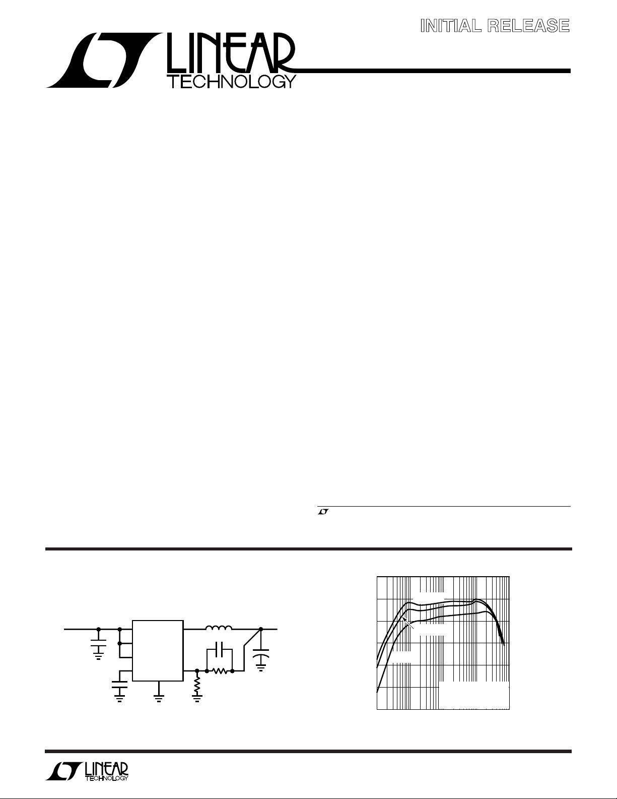
TYPICAL APPLICATIO
High Efficiency Step-Down Converter
V
IN
2.65V
TO 6V
22µF**
CER
220pF
*
TOKO D62CB A920CY-100M
**
TAIYO-YUDEN CERAMIC JMK325BJ226MM
***
SANYO POSCAP 6TPA47M
†
V
CONNECTED TO VIN FOR 2.65V < VIN < 3.3V
OUT
7
SYNC
6
V
IN
1
RUN
2
I
TH
LTC1878
GND
4
SW
U
10µH*
5
20pF
V
OUT
3.3V
†
Efficiency vs Output Load Current
+
47µF***
887k
3
V
FB
280k
1878 TA01
Information furnished by Linear Technology Corporation is believed to be accurate and reliable.
However, no responsibility is assumed for its use. Linear Technology Corporation makes no representation that the interconnection of its circuits as described herein will not infringe on existing patent rights.
1
LTC1878
1
2
3
4
8
7
6
5
TOP VIEW
MS8 PACKAGE
8-LEAD PLASTIC MSOP
PLL LPF
SYNC/MODE
V
IN
SW
RUN
I
TH
V
FB
GND
WWWU
ABSOLUTE AXI U RATI GS
PACKAGE/ORDER I FOR ATIO
UU
W
(Note 1)
Input Supply Voltage (VIN)...........................– 0.3V to 7V
ITH, PLL LPF Voltage ................................–0.3V to 2.7V
RUN, VFB Voltages ......................................–0.3V to V
SYNC/MODE Voltage ..................................–0.3V to V
IN
IN
ORDER PART
NUMBER
LTC1878EMS8
SW Voltage ................................... –0.3V to (VIN + 0.3V)
P-Channel MOSFET Source Current (DC) ........... 800mA
N-Channel MOSFET Sink Current (DC) ............... 800mA
Peak SW Sink and Source Current ........................ 1.5A
T
= 125°C, θJA = 150°C/W
JMAX
MS8 PART MARKING
LTNX
Operating Ambient Temperature Range
(Note 2) .................................................. – 40°C to 85°C
Consult factory for Industrial and Military grade parts.
Junction Temperature (Note 3)............................ 125°C
Storage Temperature Range ................. –65°C to 150°C
Lead Temperature (Soldering, 10 sec).................. 300°C
ELECTRICAL CHARACTERISTICS
The ● denotes specifications which apply over the full operating temperature range, otherwise specifications are TA = 25°C.
VIN = 3.6V unless otherwise specified.
SYMBOL PARAMETER CONDITIONS MIN TYP MAX UNITS
I
VFB
V
FB
∆V
OVL
∆V
FB
V
LOADREG
V
IN
I
Q
f
OSC
f
SYNC
I
PLL LPF
R
PFET
R
NFET
Feedback Current (Note 4) ● 430 nA
Regulated Output Voltage (Note 4) 0°C ≤ TA ≤ 85°C 0.784 0.8 0.816 V
(Note 4) –40°C ≤ T
Output Overvoltage Lockout ∆V
Reference Voltage Line Regulation VIN = 2.65V to 6V (Note 4) 0.05 0.2 %/V
Output Voltage Load Regulation Measured in Servo Loop; V
Input Voltage Range ● 2.65 6 V
Input DC Bias Current (Note 5)
Pulse Skipping Mode 2.65V < V
Burst Mode Operation V
Shutdown V
Oscillator Frequency VFB = 0.8V 495 550 605 kHz
SYNC Capture Range 400 700 kHz
Phase Detector Output Current
Sinking Capability f
Sourcing Capability f
R
of P-Channel MOSFET ISW = 100mA 0.5 0.7 Ω
DS(ON)
R
of N-Channel MOSFET ISW = –100mA 0.6 0.8 Ω
DS(ON)
= V
OVL
OVL
Measured in Servo Loop; V
IN
SYNC/MODE
= 0V, VIN = 6V 0 1 µA
RUN
V
= 0V 80 kHz
FB
< f
PLLIN
OSC
> f
PLLIN
OSC
≤ 85°C ● 0.74 0.8 0.84 V
A
– V
< 6V, V
= VIN, I
FB
= 0.9V ● 0.1 0.5 %
ITH
= 1.6V ● –0.1 –0.5 %
ITH
SYNC/MODE
OUT
= 0V, I
= 0A 10 15 µA
= 0A 230 350 µA
OUT
● 20 50 110 mV
● 3 10 20 µA
● –3 –10 –20 µA
2
LTC1878
ELECTRICAL CHARACTERISTICS
The ● denotes specifications which apply over the full operating temperature range, otherwise specifications are TA = 25°C.
VIN = 3.6V unless otherwise specified.
SYMBOL PARAMETER CONDITIONS MIN TYP MAX UNITS
I
PK
I
LSW
V
SYNC/MODE
I
SYNC/MODE
V
RUN
I
RUN
Peak Inductor Current VIN = 3.3V, VFB = 0.7V, Duty Cycle < 35% 0.8 1.0 1.25 A
SW Leakage V
SYNC/MODE Threshold V
= 0V, VSW = 0V or 6V, VIN = 6V ±0.01 ±1 µA
RUN
SYNC/MODE
Rising ● 0.2 1.0 1.5 V
SYNC/MODE Leakage Current ±0.01 ±1 µA
RUN Threshold V
Rising ● 0.2 0.7 1.5 V
RUN
RUN Input Current ±0.01 ±1 µA
Note 1: Absolute Maximum Ratings are those values beyond which the life
of a device may be impaired.
Note 2: The LTC1878E is guaranteed to meet performance specifications
from 0°C to 70°C. Specifications over the –40°C to 85°C operating
Note 4: The LTC1878 is tested in a feedback loop which servos VFB to the
balance point for the error amplifier (V
Note 5: Dynamic supply current is higher due to the gate charge being
delivered at the switching frequency.
temperature range are assured by design, characterization and correlation
with statistical process controls.
Note 3: T
dissipation P
is calculated from the ambient temperature TA and power
J
according to the following formulas:
D
LTC1878EMS8: TJ = TA + (PD)(150°C/W)
UW
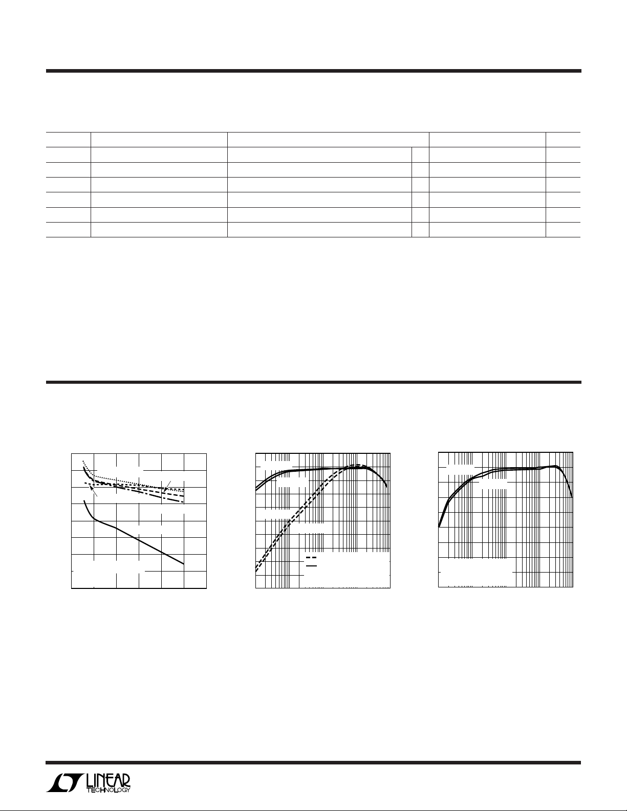
TYPICAL PERFOR A CE CHARACTERISTICS
Efficiency vs Input Voltage
100
95
90
85
80
75
EFFICIENCY (%)
70
65
60
I
= 100mA
LOAD
= 300mA
I
LOAD
I
Burst Mode OPERATION
= 2.5V
V
OUT
L = 10µH
34 6
2
INPUT VOLTAGE (V)
LOAD
= 0.1mA
5
I
LOAD
I
LOAD
= 10mA
= 1mA
7
8
1878 G01
Efficiency vs Output Current Efficiency vs Output Current
100
VIN = 3.6V
90
80
70
60
50
40
EFFICIENCY (%)
30
20
10
0
VIN = 4.2V
VIN = 3.6V
VIN = 4.2V
PULSE SKIPPING MODE
Burst Mode OPERATION
= 1.8V
V
OUT
L = 10µH
0.1 10 100 1000
1
OUTPUT CURRENT (mA)
1878 G02
= 1.2V).
ITH
95
90
L = 15µH
85
80
75
70
EFFICIENCY (%)
65
60
Burst Mode OPERATION
55
V
IN
V
OUT
50
0.1 10 100 1000
L = 10µH
= 6V
= 2.5V
1
OUTPUT CURRENT (mA)
1878 G03
3
LTC1878
TEMPERATURE (°C)
–50
300
250
200
150
100
50
0
25 75
1878 G12
–25 0
50 125100
SUPPLY CURRENT (µA)
PULSE SKIPPING
MODE
Burst Mode
OPERATION
VIN = 3.6V
UW
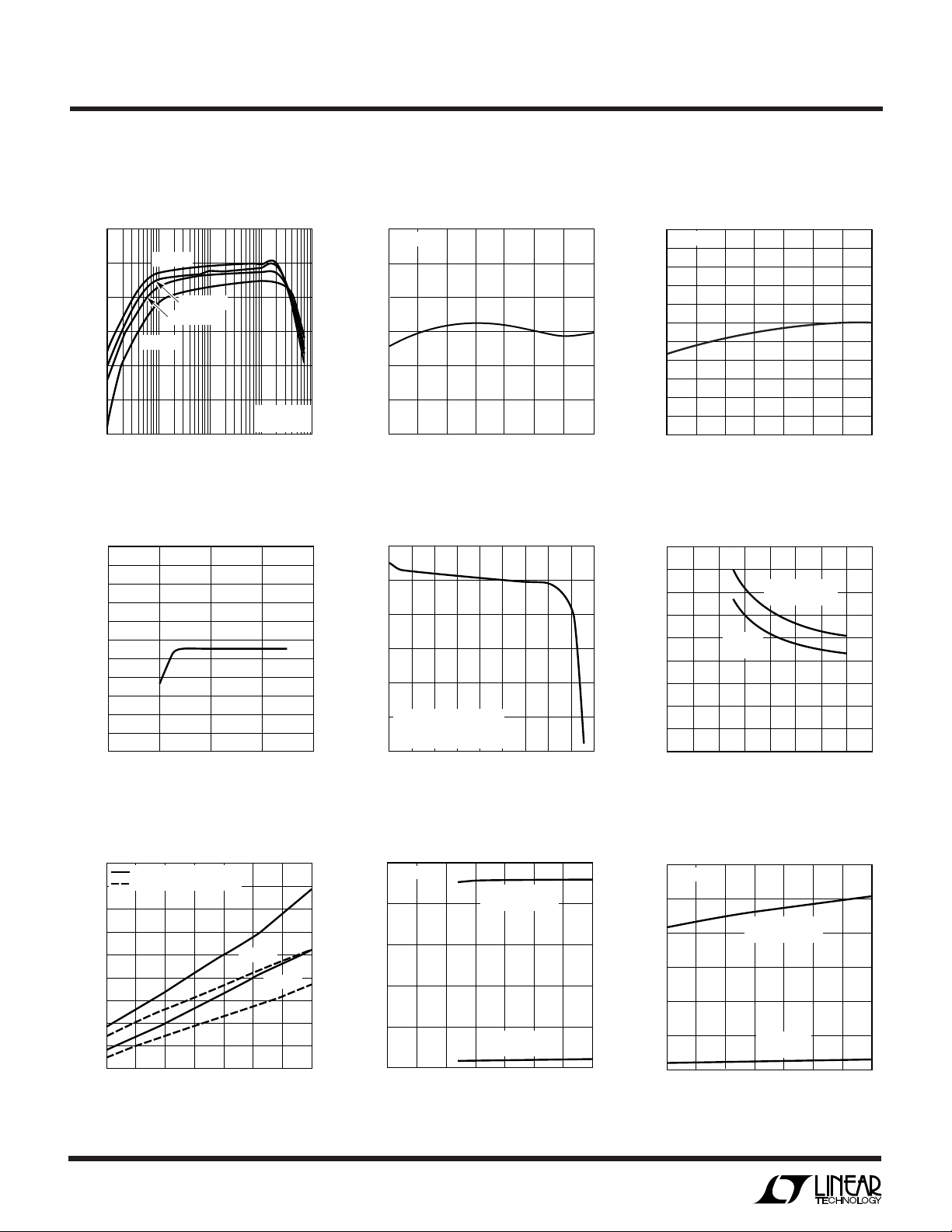
TYPICAL PERFOR A CE CHARACTERISTICS
Efficiency vs Output Current
95
90
85
80
EFFICIENCY (%)
75
70
65
0.1 10 100 1000
VIN = 3V
VIN = 3.6V
VIN = 4.2V
VIN = 6V
1
OUTPUT CURRENT (mA)
V
OUT
L = 10µH
Oscillator Frequency
vs Supply Voltage
605
595
585
575
565
555
545
535
525
515
OSCILLATOR FREQUENCY (kHz)
505
495
0
2
4
SUPPLY VOLTAGE (V)
6
= 1.8V
1878 G04
1878 G07
0.814
0.809
0.804
0.799
0.794
REFERENCE VOLTAGE (V)
0.789
0.784
1.83
1.82
1.81
1.80
1.79
OUTPUT VOLTAGE (V)
1.78
8
1.77
Reference Voltage
Reference Voltage
vs Temperature
vs Temperature
VIN = 3.6V
–50
–25 0
50 100 125
25 75
TEMPERATURE (°C)
1878 G05
605
595
585
575
565
555
545
535
FREQUENCY (kHz)
525
515
505
495
Output Voltage vs Load Current R
0.9
0.8
0.7
0.6
(Ω)
0.5
0.4
DS(ON)
R
0.3
PULSE SKIPPING MODE
V
= 3.6V
IN
L = 10µH
100 300
200
0
400
LOAD CURRENT (mA)
700
600
800
1878 G08
500 900
0.2
0.1
Oscillator Frequency
vs Temperature
VIN = 3.6V
–25
–50
DS(ON)
0
0
TEMPERATURE (°C)
vs Input Voltage
MAIN
SWITCH
10
3
2
INPUT VOLTAGE (V)
5025
SYNCHRONOUS
SWITCH
5678
4
10075
125
1878 G06
1878 G09
DC Supply Current
R
vs Temperature
DS(ON)
1.2
SYNCHRONOUS SWITCH
MAIN SWITCH
1.1
1.0
0.9
(Ω)
0.8
0.7
DS(ON)
R
0.6
0.5
0.4
0.3
4
–50 –25
0 25 50 125
TEMPERATURE (°C)
VIN = 3V
VIN = 5V
75 100
1878 G10
vs Input Voltage
250
V
= 1.8V
OUT
200
150
100
DC SUPPLY CURRENT (µA)
50
0
01
PULSE SKIPPING
MODE
Burst Mode
OPERATION
4
3
2
INPUT VOLTAGE (V)
6
7
1878 G11
5
DC Supply Current
vs Temperature
UW
TYPICAL PERFOR A CE CHARACTERISTICS
LTC1878
Switch Leakage vs Temperature
2.5
VIN = 7V
RUN = 0V
2.0
1.5
1.0
SWITCH LEAKAGE (µA)
0.5
0
–25 0 50
–50
SYNCHRONOUS
25
TEMPERATURE (°C)
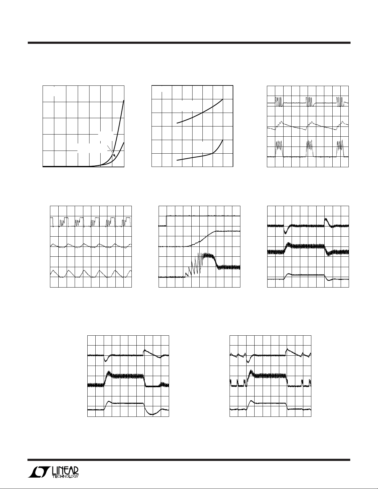
Pulse Skipping Mode Operation
SW
5V/DIV
V
OUT
20mV/DIV
AC
COUPLED
I
L
200mA/DIV
MAIN
SWITCH
SWITCH
75 100 125
1878 G13
1.2
RUN = 0V
1.0
0.8
0.6
0.4
SWITCH LEAKAGE (nA)
0.2
0
13
0
Start-Up from Shutdown Load Step Response
RUN
2V/DIV
V
OUT
1V/DIV
I
L
500mA/DIV
SYNCHRONOUS
SWITCH
MAIN
SWITCH
24
INPUT VOLTAGE (V)
5
Burst Mode OperationSwitch Leakage vs Input Voltage
SW
5V/DIV
V
OUT
50mV/DIV
AC
COUPLED
I
L
200mA/DIV
6
7
1878 G20
8
V
OUT
50mV/DIV
COUPLED
500mA/DIV
1V/DIV
AC
I
L
I
TH
V
= 4.2V
IN
V
= 1.5V
OUT
L = 10µH
C
IN
C
OUT
I
LOAD
10µs/DIV
= 22µF
= 47µF
= 50mA
1878 G14
V
= 4.2V
IN
V
= 1.5V
OUT
L = 10µH
C
IN
C
OUT
I
LOAD
V
OUT
100mV/DIV
COUPLED
500mA/DIV
I
1V/DIV
1µs/DIV
= 22µF
= 47µF
= 50mA
Load Step Response
AC
I
L
TH
V
= 3.6V
IN
= 1.5V
V
OUT
L = 10µH
= 22µF
C
IN
C
OUT
I
LOAD
PULSE SKIPPING MODE
1878 G15
40µs/DIV
= 47µF
= 50mA TO 500mA
= 3.6V
V
IN
= 1.5V
V
OUT
L = 10µH
1878 G18
C
C
I
LOAD
IN
OUT
40µs/DIV
= 22µF
= 47µF
= 500mA
V
OUT
100mV/DIV
COUPLED
500mA/DIV
I
1V/DIV
1878 G16
Load Step Response
AC
I
L
TH
V
= 3.6V
IN
= 1.5V
V
OUT
L = 10µH
= 22µF
C
IN
C
OUT
I
LOAD
Burst Mode OPERATION
V
= 3.6V
IN
= 1.5V
V
OUT
L = 10µH
40µs/DIV
= 47µF
= 50mA TO 500mA
40µs/DIV
= 22µF
C
IN
= 47µF
C
OUT
I
= 200mA TO 500mA
LOAD
PULSE SKIPPING MODE
1878 G19
1878 G17
5
 Loading...