

LTC1871
FEATURES
■
High Efficiency (No Sense Resistor Required)
■
Wide Input Voltage Range: 2.5V to 36V
■
Current Mode Control Provides Excellent
Transient Response
■
High Maximum Duty Cycle (92% Typ)
■
±2% RUN Pin Threshold with 100mV Hysteresis
■
±1% Internal Voltage Reference
■
Micropower Shutdown: IQ = 10µA
■
Programmable Operating Frequency
(50kHz to 1MHz) with One External Resistor
■
Synchronizable to an External Clock Up to 1.3 × f
■
User-Controlled Pulse Skip or Burst Mode® Operation
■
Internal 5.2V Low Dropout Voltage Regulator
■
Output Overvoltage Protection
■
Capable of Operating with a Sense Resistor for High
Output Voltage Applications
■
Small 10-Lead MSOP Package
U
APPLICATIO S
■
Telecom Power Supplies
■
Portable Electronic Equipment
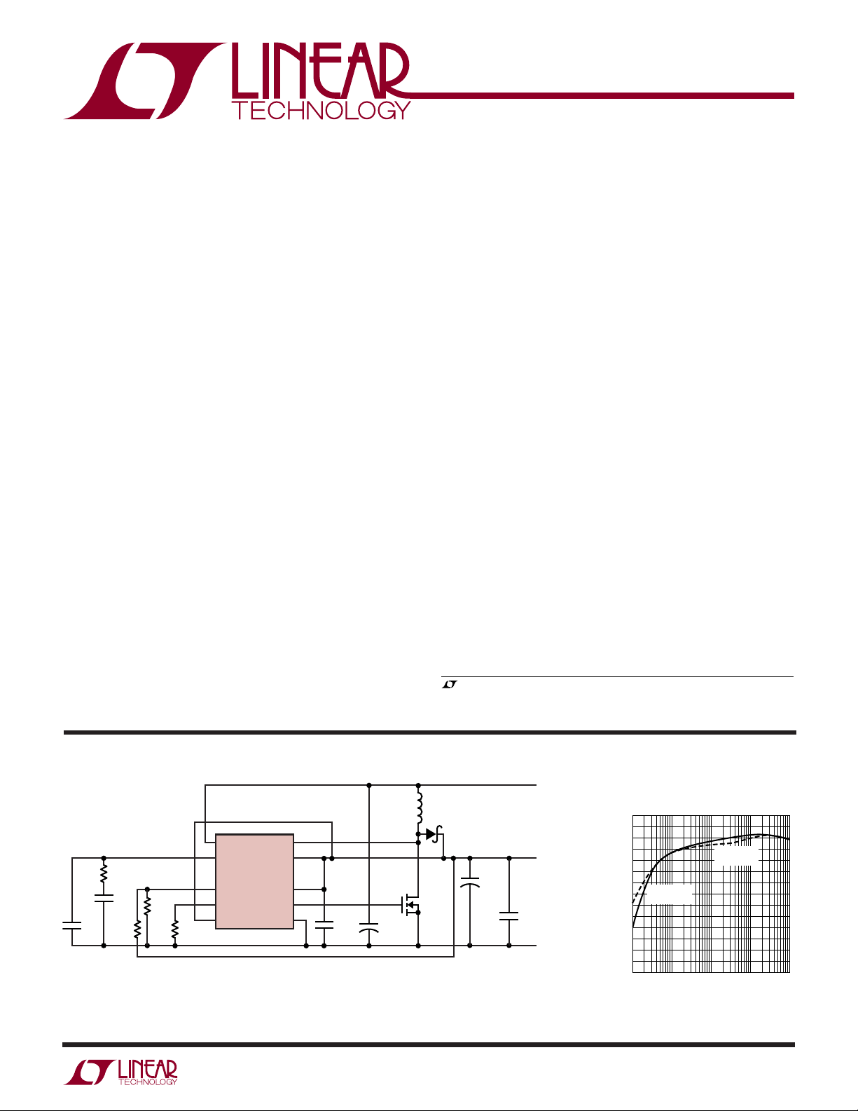
OSC
Wide Input Range, No R
SENSE
Current Mode Boost,
Flyback and SEPIC Controller
U
DESCRIPTIO
The LTC®1871 is a wide input range, current mode, boost,
flyback or SEPIC controller that drives an N-channel
power MOSFET and requires very few external components. Intended for low to medium power applications, it
eliminates the need for a current sense resistor by utilizing the power MOSFET’s on-resistance, thereby maximizing efficiency.
The IC’s operating frequency can be set with an external
resistor over a 50kHz to 1MHz range, and can be synchronized to an external clock using the MODE/SYNC pin.
Burst Mode operation at light loads, a low minimum
operating supply voltage of 2.5V and a low shutdown
quiescent current of 10µA make the LTC1871 ideally
suited for battery-operated systems.
For applications requiring constant frequency operation,
Burst Mode operation can be defeated using the MODE/
SYNC pin. Higher output voltage boost, SEPIC and flyback applications are possible with the LTC1871 by
connecting the SENSE pin to a resistor in the source of the
power MOSFET.
The LTC1871 is available in the 10-lead MSOP package.
, LTC and LT are registered trademarks of Linear Technology Corporation.
TM
Burst Mode is a registered trademark of Linear Technology Corporation. No R
of Linear Technology Corporation. All other trademarks are the property of their respective owners.
is a trademark
SENSE
TYPICAL APPLICATIO
RUN
I
R
T
80.6k
1%
TH
LTC1871
FB
FREQ
MODE/SYNC
R
C
22k
C
R1
C1
6.8nF
12.1k
1%
R2
C
C2
37.4k
47pF
1%
CIN: TAIYO YUDEN JMK325BJ226MM
: PANASONIC EEFUEOJ151R
C
OUT1
: TAIYO YUDEN JMK325BJ226MM
C
OUT2
Figure 1. High Efficiency 3.3V Input, 5V Output Boost Converter (Bootstrapped)
U
SENSE
V
IN
INTV
CC
GATE
GND
D1: MBRB2515L
L1: SUMIDA CEP125-H 1R0MH
M1: FAIRCHILD FDS7760A
C
VCC
4.7µF
X5R
V
IN
C
22µF
6.3V
X5R
×2
1871 F01a
3.3V
V
5V
7A
(10A PEAK)
OUT2
GND
OUT
EFFICIENCY (%)
L1
1µH
D1
C
OUT1
+
150µF
6.3V
M1
C
IN
+
22µF
6.3V
×2
×4
Efficiency of Figure 1
100
90
80
70
PULSE-SKIP
MODE
60
50
40
30
0.01
0.001 0.1 1 10
OUTPUT CURRENT (A)
Burst Mode
OPERATION
1871 F01b
1871fc
1
LTC1871
1
2
3
4
5
RUN
I
TH
FB
FREQ
MODE/
SYNC
10
9
8
7
6
SENSE
V
IN
INTV
CC
GATE
GND
TOP VIEW
MS PACKAGE
10-LEAD PLASTIC MSOP
WWWU
ABSOLUTE AXI U RATI GS
PACKAGE/ORDER I FOR ATIO
UU
W
(Note 1)
VIN Voltage ............................................... –0.3V to 36V
INTV
INTV
GATE Voltage ........................... – 0.3V to V
I
RUN, MODE/SYNC Voltages ....................... –0.3V to 7V
Voltage ........................................... –0.3V to 7V
CC
Output Current ........................................ 50mA
CC
+ 0.3V
INTVCC
, FB Voltages ....................................... – 0.3V to 2.7V
TH
T
= 125°C, θJA = 120°C/ W
JMAX
FREQ Voltage ............................................– 0.3V to 1.5V
SENSE Pin Voltage ................................... – 0.3V to 36V
Operating Junction Temperature Range (Note 2)
LTC1871E ........................................... – 40°C to 85°C
LTC1871I.......................................... – 40°C to 125°C
Junction Temperature (Note 3)............................ 125°C
Storage Temperature Range ................. –65°C to 150°C
Lead Temperature (Soldering, 10 sec).................. 300°C
ELECTRICAL CHARACTERISTICS
range, otherwise specifications are at TA = 25°C. VIN = V
SYMBOL PARAMETER CONDITIONS MIN TYP MAX UNITS
Main Control Loop
V
IN(MIN)
I
Q
+
V
RUN
–
V
RUN
V
RUN(HYST)
I
RUN
V
FB
I
FB
∆V
FB
∆V
IN
2
Minimum Input Voltage 2.5 V
Input Voltage Supply Current (Note 4)
Continuous Mode V
Burst Mode Operation, No Load V
Shutdown Mode V
Rising RUN Input Threshold Voltage 1.348 V
Falling RUN Input Threshold Voltage 1.223 1.248 1.273 V
RUN Pin Input Threshold Hysteresis 50 100 150 mV
RUN Input Current 160 nA
Feedback Voltage V
FB Pin Input Current V
Line Regulation 2.5V ≤ VIN ≤ 30V 0.002 0.02 %/V
The ● denotes specifications which apply over the full operating temperature
= 5V, V
INTVCC
I-Grade (Note 2)
MODE/SYNC
V
MODE/SYNC
I-Grade (Note 2)
MODE/SYNC
V
MODE/SYNC
I-Grade (Note 2)
RUN
V
RUN
I-Grade (Note 2)
ITH
V
ITH
ITH
2.5V ≤ VIN ≤ 30V, I-Grade (Note 2)
= 5V, VFB = 1.4V, V
= 5V, VFB = 1.4V, V
= 0V, V
= 0V, V
= 0V 10 20 µA
= 0V, I-Grade (Note 2)
= 0.2V (Note 5) 1.218 1.230 1.242 V
= 0.2V (Note 5), I-Grade (Note 2)
= 0.2V (Note 5) 18 60 nA
ORDER PART NUMBER
LTC1871EMS
LTC1871IMS
Order Options Tape and Reel: Add #TR
Lead Free: Add #PBF Lead Free Tape and Reel: Add #TRPBF
Lead Free Part Marking: http://www.linear.com/leadfree/
Consult LTC Marketing for parts specified with wider operating temperature ranges.
= 1.5V, R
RUN
= 0.2V (Note 5) 250 500 µA
ITH
= 0.2V (Note 5),
ITH
= 80k, V
FREQ
= 0.75V 550 1000 µA
ITH
= 0.75V,
ITH
MODE/SYNC
●
●
●
●
●
●
●
●
●
MS PART MARKING
LTSX
LTBFC
= 0V, unless otherwise specified.
2.5 V
550 1000 µA
250 500 µA
10 20 µA
1.198 1.298 V
35 100 175 mV
1.212 1.248 V
1.205 1.255 V
0.002 0.02 %/V
1871fc
LTC1871
ELECTRICAL CHARACTERISTICS
range, otherwise specifications are at T
= 25°C. VIN = V
A
The ● denotes specifications which apply over the full operating temperature
INTVCC
= 5V, V
= 1.5V, R
RUN
FREQ
= 80k, V
MODE/SYNC
= 0V, unless otherwise specified.
SYMBOL PARAMETER CONDITIONS MIN TYP MAX UNITS
∆V
∆V
FB
ITH
Load Regulation V
MODE/SYNC
V
MODE/SYNC
= 0V, V
= 0V, V
= 0.5V to 0.9V (Note 5)
ITH
= 0.5V to 0.9V (Note 5)
ITH
●
–1 –0.1 %
●
–1 –0.1 %
I-Grade (Note 2)
∆V
FB(OV)
g
m
V
ITH(BURST)
V
SENSE(MAX)
I
SENSE(ON)
I
SENSE(OFF)
∆FB Pin, Overvoltage Lockout V
FB(OV)
– V
in Percent 2.5 6 10 %
FB(NOM)
Error Amplifier Transconductance ITH Pin Load = ±5µA (Note 5) 650 µmho
Burst Mode Operation ITH Pin Voltage Falling ITH Voltage (Note 5) 0.3 V
Maximum Current Sense Input Threshold Duty Cycle < 20% 120 150 180 mV
SENSE Pin Current (GATE High) V
SENSE Pin Current (GATE Low) V
Duty Cycle < 20%, I-Grade (Note 2)
= 0V 35 50 µA
SENSE
= 30V 0.1 5 µA
SENSE
●
100 200 mV
Oscillator
f
OSC
Oscillator Frequency R
= 80k 250 300 350 kHz
FREQ
R
= 80k, I-Grade (Note 2)
FREQ
●
250 300 350 kHz
Oscillator Frequency Range 50 1000 kHz
D
MAX
f
SYNC/fOSC
I-Grade (Note 2)
Maximum Duty Cycle 87 92 97 %
I-Grade (Note 2)
Recommended Maximum Synchronized f
= 300kHz (Note 6) 1.25 1.30
OSC
●
50 1000 kHz
●
87 92 97 %
Frequency Ratio
f
t
SYNC(MIN)
t
SYNC(MAX)
V
IL(MODE)
V
IH(MODE)
R
MODE/SYNC
V
FREQ
= 300kHz (Note 6), I-Grade (Note 2)
OSC
MODE/SYNC Minimum Input Pulse Width V
MODE/SYNC Maximum Input Pulse Width V
= 0V to 5V 25 ns
SYNC
= 0V to 5V 0.8/f
SYNC
Low Level MODE/SYNC Input Voltage 0.3 V
I-Grade (Note 2)
High Level MODE/SYNC Input Voltage 1.2 V
I-Grade (Note 2)
MODE/SYNC Input Pull-Down Resistance 50 kΩ
Nominal FREQ Pin Voltage 0.62 V
●
●
●
1.2 V
1.25 1.30
OSC
0.3 V
ns
Low Dropout Regulator
V
INTVCC
∆V
INTVCC
∆V
IN1
∆V
INTVCC
∆V
IN2
V
LDO(LOAD)
V
DROPOUT
I
INTVCC
INTVCC Regulator Output Voltage VIN = 7.5V 5.0 5.2 5.4 V
VIN = 7.5V, I-Grade (Note 2)
●
5.0 5.2 5.4 V
INTVCC Regulator Line Regulation 7.5V ≤ VIN ≤ 15V 8 25 mV
INTVCC Regulator Line Regulation 15V ≤ VIN ≤ 30V 70 200 mV
INTVCC Load Regulation 0 ≤ I
≤ 20mA, VIN = 7.5V –2 –0.2 %
INTVCC
INTVCC Regulator Dropout Voltage VIN = 5V, INTVCC Load = 20mA 280 mV
Bootstrap Mode INTVCC Supply RUN = 0V, SENSE = 5V 10 20 µA
Current in Shutdown
I-Grade (Note 2)
●
30 µA
GATE Driver
t
r
t
f
GATE Driver Output Rise Time CL = 3300pF (Note 7) 17 100 ns
GATE Driver Output Fall Time CL = 3300pF (Note 7) 8 100 ns
1871fc
3
LTC1871
ELECTRICAL CHARACTERISTICS
range, otherwise specifications are at T
Note 1: Absolute Maximum Ratings are those values beyond which the life
of the device may be impaired.
Note 2: The LTC1871E is guaranteed to meet performance specifications
from 0°C to 70°C junction temperature. Specifications over the –40°C to
85°C operating junction temperature range are assured by design,
characterization and correlation with statistical process controls. The
LTC1871I is guaranteed over the full –40°C to 125°C operating junction
temperature range.
Note 3: T
dissipation P
is calculated from the ambient temperature TA and power
J
according to the following formula:
D
= TA + (PD • 110°C/W)
T
J
= 25°C. VIN = V
A
The ● denotes specifications which apply over the full operating temperature
INTVCC
= 5V, V
= 1.5V, R
RUN
FREQ
= 80k, V
MODE/SYNC
= 0V, unless otherwise specified.
Note 4: The dynamic input supply current is higher due to power MOSFET
gate charging (Q
• f
). See Applications Information.
G
OSC
Note 5: The LTC1871 is tested in a feedback loop which servos V
reference voltage with the I
range (0.3V ≤ V
≤ 1.2V, midpoint = 0.75V).
ITH
pin forced to the midpoint of its voltage
TH
Note 6: In a synchronized application, the internal slope compensation
gain is increased by 25%. Synchronizing to a significantly higher ratio will
reduce the effective amount of slope compensation, which could result in
subharmonic oscillation for duty cycles greater than 50%.
Note 7: Rise and fall times are measured at 10% and 90% levels.
UW
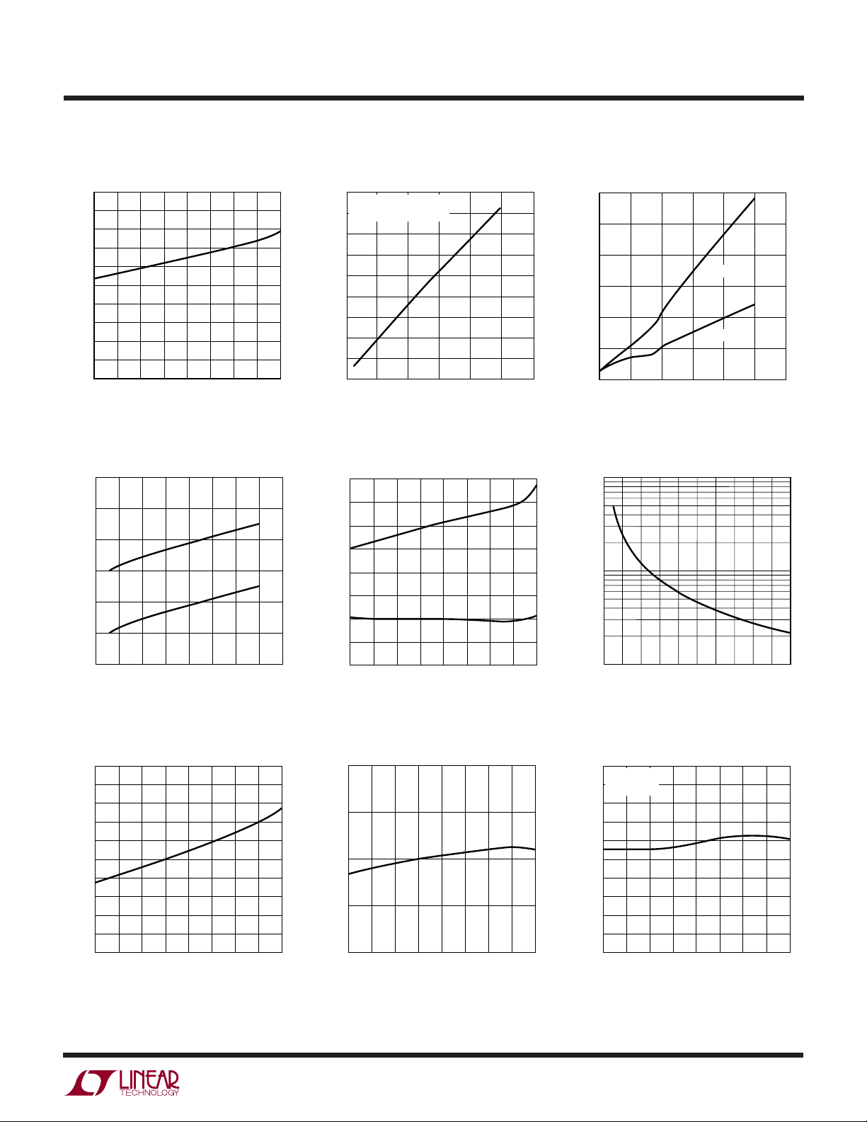
TYPICAL PERFOR A CE CHARACTERISTICS
FB Voltage vs Temp FB Voltage Line Regulation FB Pin Current vs Temperature
1.25
1.24
1.231
60
50
40
to the
FB
1.23
FB VOLTAGE (V)
1.22
1.21
–25
–50
0
TEMPERATURE (°C)
Shutdown Mode IQ vs V
30
(µA)
Q
20
10
SHUTDOWN MODE I
0
0
10 20
25
50
VIN (V)
1.230
FB VOLTAGE (V)
75
100
IN
30
125
1871 G01
150
1871 G04
1.229
(µA)
Q
SHUTDOWN MODE I
40
5101520
0
VIN (V)
25 30 35
Shutdown Mode IQ vs Temperature
20
VIN = 5V
15
10
5
0
–50
–25 0 25 50
TEMPERATURE (°C)
75 100 125 150
1871 G02
1871 G05
30
20
FB PIN CURRENT (nA)
10
0
–50
–25
Burst Mode IQ vs V
600
500
400
(µA)
Q
300
200
Burst Mode I
100
0
0
10 20
250 50 10075
TEMPERATURE (°C)
IN
VIN (V)
125 150
1871 G03
30 40
1871 G06
4
1871fc
UW
TEMPERATURE (°C)
–50
25
SENSE PIN CURRENT (µA)
30
35
0
50
75
1871 G15
–25 25
100
125
150
GATE HIGH
V
SENSE
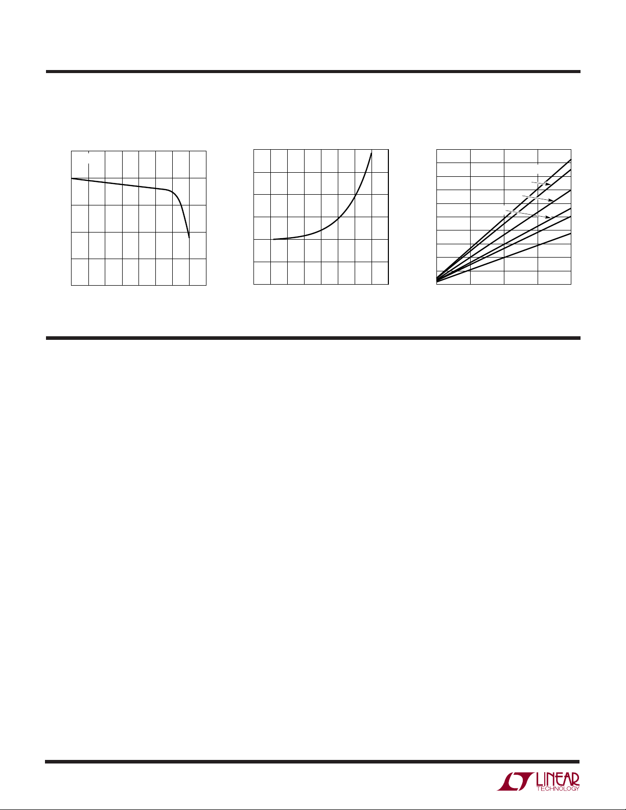
= 0V
TYPICAL PERFOR A CE CHARACTERISTICS
Burst Mode IQ vs Temperature
500
400
(µA)
300
Q
200
Burst Mode I
100
0
–50
–25 25
0
50
TEMPERATURE (°C)
125
100
75
150
1871 G07
Dynamic IQ vs Frequency
18
CL = 3300pF
= 550µA + Qg • f
I
16
Q(TOT)
14
12
10
(mA)
Q
8
I
6
4
2
0
0
400 1200
200 1000
FREQUENCY (kHz)
600
800
1871 G08
LTC1871
Gate Drive Rise and Fall Time
vs C
L
60
50
40
RISE TIME
30
TIME (ns)
20
10
0
0
4000 6000 8000
2000
FALL TIME
CL (pF)
10000 12000
1871 G09
RUN Thresholds vs V
1.5
1.4
1.3
RUN THRESHOLDS (V)
1.2
0
Frequency vs Temperature
325
320
315
310
305
300
295
290
GATE FREQUENCY (kHz)
285
280
275
–50
10 20
–25 25
0
TEMPERATURE (°C)
VIN (V)
50
IN
30
40
1871 G10
RUN Thresholds vs Temperature
1.40
1.35
1.30
RUN THRESHOLDS (V)
1.25
1.20
–50
–25
0
50
25
TEMPERATURE (°C)
75
100
125
1871 G11
150
RT vs Frequency
1000
100
(kΩ)
T
R
10
100
0
200 1000
400
500
300
FREQUENCY (kHz)
800700600
900
1871 G12
Maximum Sense Threshold
vs Temperature
160
155
150
145
MAX SENSE THRESHOLD (mV)
140
–50
125
100
75
150
1871 G13
–25 0 25 50
TEMPERATURE (°C)
75 100 125 150
1871 G14
SENSE Pin Current vs Temperature
1871fc
5
LTC1871
UW
TYPICAL PERFOR A CE CHARACTERISTICS
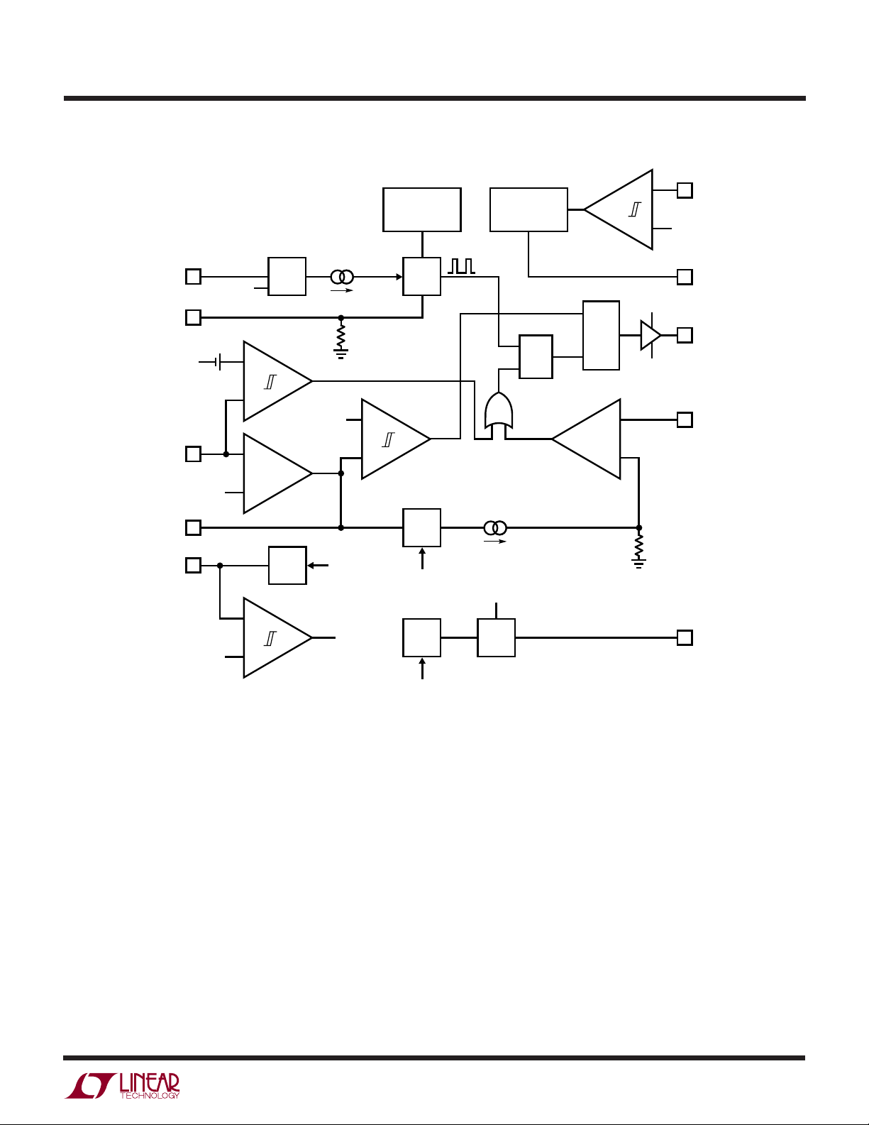
INTVCC Load Regulation
VIN = 7.5V
5.2
VOLTAGE (V)
CC
5.1
INTV
5.0
0
10 20
30 50 80
INTVCC LOAD (mA)
40
60 70
1871 G16
INTV
5.4
5.3
VOLTAGE (V)
CC
5.2
INTV
5.1
0
Line Regulation
CC
515
10 20
VIN (V)
25
30
35
1871 G17
INTV
Dropout Voltage
CC
vs Current, Temperature
500
450
400
350
300
250
200
150
DROPOUT VOLTAGE (mV)
100
50
40
0
0
25°C
5
10
INTVCC LOAD (mA)
125°C
75°C
150°C
–50°C
15
0°C
20
1871 G18
U
UU
PI FU CTIO S
RUN (Pin 1): The RUN pin provides the user with an
accurate means for sensing the input voltage and programming the start-up threshold for the converter. The
falling RUN pin threshold is nominally 1.248V and the
comparator has 100mV of hysteresis for noise immunity.
When the RUN pin is below this input threshold, the IC is
shut down and the V
value (typ 10µA). The Absolute Maximum Rating for the
voltage on this pin is 7V.
I
(Pin 2): Error Amplifier Compensation Pin. The cur-
TH
rent comparator input threshold increases with this
control voltage. Nominal voltage range for this pin is 0V
to 1.40V.
FB (Pin 3): Receives the feedback voltage from the
external resistor divider across the output. Nominal
voltage for this pin in regulation is 1.230V.
FREQ (Pin 4): A resistor from the FREQ pin to ground
programs the operating frequency of the chip. The nominal voltage at the FREQ pin is 0.6V.
MODE/SYNC (Pin 5): This input controls the operating
mode of the converter and allows for synchronizing the
supply current is kept to a low
IN
operating frequency to an external clock. If the MODE/
SYNC pin is connected to ground, Burst Mode operation
is enabled. If the MODE/SYNC pin is connected to INTV
, or if an external logic-level synchronization signal
CC
is applied to this input, Burst Mode operation is disabled
and the IC operates in a continuous mode.
GND (Pin 6): Ground Pin.
GATE (Pin 7): Gate Driver Output.
I
NTVCC (Pin 8): The Internal 5.20V Regulator Output. The
gate driver and control circuits are powered from this
voltage. Decouple this pin locally to the IC ground with a
minimum of 4.7µF low ESR tantalum or ceramic
capacitor.
V
(Pin 9): Main Supply Pin. Must be closely decoupled
IN
to ground.
SENSE (Pin 10): The Current Sense Input for the Control
Loop. Connect this pin to the drain of the power MOSFET
for V
sensing and highest efficiency. Alternatively, the
DS
SENSE pin may be connected to a resistor in the source
of the power MOSFET. Internal leading edge blanking is
provided for both sensing methods.
6
1871fc
BLOCK DIAGRA
W
SLOPE
COMPENSATION
BIAS AND
START-UP
CONTROL
LTC1871
RUN
1
+
C2
1.248V
–
FREQ
4
MODE/SYNC
5
85mV
1.230V
FB
3
1.230V
I
TH
2
INTV
CC
8
2.00V
V
IN
0.6V
OV
–
+
I
OSC
50k
+
+
–
1.230V
TO
START-UP
CONTROL
5.2V
0.30V
EA
–
g
m
+
LDO
UV
–
+
OSCV-TO-I
BURST
COMPARATOR
V-TO-I
SLOPE
BIAS V
I
LOOP
1.230V
REF
PWM LATCH
S
Q
R
CURRENT
COMPARATOR
INTV
LOGIC
+
C1
–
GND
R
9
CC
GATE
7
SENSE
10
LOOP
GND
6
1871 BD
V
IN
1871fc
7

LTC1871
OPERATIO
U
Main Control Loop
The LTC1871 is a constant frequency, current mode
controller for DC/DC boost, SEPIC and flyback converter
applications. The LTC1871 is distinguished from conventional current mode controllers because the current control loop can be closed by sensing the voltage drop across
the power MOSFET switch instead of across a discrete
sense resistor, as shown in Figure 2. This sensing technique improves efficiency, increases power density, and
reduces the cost of the overall solution.
D
V
OUT
+
C
V
SW
V
SW
R
OUT
D
V
OUT
+
C
OUT
S
1871 F02
V
IN
SENSE
GATE
GND
V
IN
GATE
SENSE
GND
L
L
V
IN
GND
2a. SENSE Pin Connection for
Maximum Efficiency (VSW < 36V)
V
IN
GND
2b. SENSE Pin Connection for Precise
Control of Peak Current or for VSW > 36V
Figure 2. Using the SENSE Pin On the LTC1871
to rise, which causes the current comparator C1 to trip at
a higher peak inductor current value. The average inductor
current will therefore rise until it equals the load current,
thereby maintaining output regulation.
The nominal operating frequency of the LTC1871 is programmed using a resistor from the FREQ pin to ground
and can be controlled over a 50kHz to 1000kHz range. In
addition, the internal oscillator can be synchronized to an
external clock applied to the MODE/SYNC pin and can be
locked to a frequency between 100% and 130% of its
nominal value. When the MODE/SYNC pin is left open, it is
pulled low by an internal 50k resistor and Burst Mode
operation is enabled. If this pin is taken above 2V or an
external clock is applied, Burst Mode operation is disabled
and the IC operates in continuous mode. With no load (or
an extremely light load), the controller will skip pulses in
order to maintain regulation and prevent excessive output
ripple.
The RUN pin controls whether the IC is enabled or is in a
low current shutdown state. A micropower 1.248V reference and comparator C2 allow the user to program the
supply voltage at which the IC turns on and off (comparator C2 has 100mV of hysteresis for noise immunity). With
the RUN pin below 1.248V, the chip is off and the input
supply current is typically only 10µA.
An overvoltage comparator OV senses when the FB pin
exceeds the reference voltage by 6.5% and provides a
reset pulse to the main RS latch. Because this RS latch is
reset-dominant, the power MOSFET is actively held off for
the duration of an output overvoltage condition.
For circuit operation, please refer to the Block Diagram of
the IC and Figure 1. In normal operation, the power
MOSFET is turned on when the oscillator sets the PWM
latch and is turned off when the current comparator C1
resets the latch. The divided-down output voltage is compared to an internal 1.230V reference by the error amplifier
EA, which outputs an error signal at the ITH pin. The voltage
on the I
pin sets the current comparator C1 input
TH
threshold. When the load current increases, a fall in the FB
voltage relative to the reference voltage causes the I
TH
pin
8
The LTC1871 can be used either by sensing the voltage
drop across the power MOSFET or by connecting the
SENSE pin to a conventional shunt resistor in the source
of the power MOSFET, as shown in Figure 2. Sensing the
voltage across the power MOSFET maximizes converter
efficiency and minimizes the component count, but limits
the output voltage to the maximum rating for this pin
(36V). By connecting the SENSE pin to a resistor in the
source of the power MOSFET, the user is able to program
output voltages significantly greater than 36V.
1871fc
OPERATIO
LTC1871
U
Programming the Operating Mode
For applications where maximizing the efficiency at very
light loads (e.g., <100µA) is a high priority, the current in
the output divider could be decreased to a few microamps and Burst Mode operation should be applied (i.e.,
the MODE/SYNC pin should be connected to ground). In
applications where fixed frequency operation is more
critical than low current efficiency, or where the lowest
output ripple is desired, pulse-skip mode operation should
be used and the MODE/SYNC pin should be connected to
the INTVCC pin. This allows discontinuous conduction
mode (DCM) operation down to near the limit defined by
the chip’s minimum on-time (about 175ns). Below this
output current level, the converter will begin to skip
cycles in order to maintain output regulation. Figures 3
and 4 show the light load switching waveforms for Burst
Mode and pulse-skip mode operation for the converter in
Figure 1.
Burst Mode Operation
Burst Mode operation is selected by leaving the MODE/
SYNC pin unconnected or by connecting it to ground. In
normal operation, the range on the ITH pin corresponding
to no load to full load is 0.30V to 1.2V. In Burst Mode
operation, if the error amplifier EA drives the I
below 0.525V, the buffered I
input to the current com-
TH
voltage
TH
parator C1 will be clamped at 0.525V (which corresponds
to 25% of maximum load current). The inductor current
peak is then held at approximately 30mV divided by the
power MOSFET R
. If the ITH pin drops below 0.30V,
DS(ON)
the Burst Mode comparator B1 will turn off the power
MOSFET and scale back the quiescent current of the IC to
250µA (sleep mode). In this condition, the load current will
be supplied by the output capacitor until the I
voltage
TH
rises above the 50mV hysteresis of the burst comparator.
At light loads, short bursts of switching (where the average inductor current is 20% of its maximum value) followed by long periods of sleep will be observed, thereby
greatly improving converter efficiency. Oscilloscope waveforms illustrating Burst Mode operation are shown in
Figure 3.
Pulse-Skip Mode Operation
With the MODE/SYNC pin tied to a DC voltage above 2V,
Burst Mode operation is disabled. The internal, 0.525V
buffered I
burst clamp is removed, allowing the ITH pin
TH
to directly control the current comparator from no load to
full load. With no load, the I
pin is driven below 0.30V,
TH
the power MOSFET is turned off and sleep mode is
invoked. Oscilloscope waveforms illustrating this mode of
operation are shown in Figure 4.
When an external clock signal drives the MODE/SYNC pin
at a rate faster than the chip’s internal oscillator, the
oscillator will synchronize to it. In this synchronized mode,
Burst Mode operation is disabled. The constant frequency
associated with synchronized operation provides a more
controlled noise spectrum from the converter, at the
expense of overall system efficiency of light loads.
VIN = 3.3V
= 5V
V
OUT
= 500mA
I
OUT
V
OUT
50mV/DIV
I
L
5A/DIV
Figure 3. LTC1871 Burst Mode Operation
(MODE/SYNC = 0V) at Low Output Current
MODE/SYNC = 0V
(Burst Mode OPERATION)
10µs/DIV 1871 F03
VIN = 3.3V
= 5V
V
OUT
= 500mA
I
OUT
V
OUT
50mV/DIV
I
L
5A/DIV
Figure 4. LTC1871 Low Output Current Operation with Burst
Mode Operation Disabled (MODE/SYNC = INTV
MODE/SYNC = INTV
(PULSE-SKIP MODE)
2µs/DIV
CC
1871 F04
)
CC
1871fc
9
LTC1871
WUUU
APPLICATIO S I FOR ATIO
When the oscillator’s internal logic circuitry detects a
synchronizing signal on the MODE/SYNC pin, the internal
oscillator ramp is terminated early and the slope compensation is increased by approximately 30%. As a result, in
applications requiring synchronization, it is recommended
that the nominal operating frequency of the IC be programmed to be about 75% of the external clock frequency.
Attempting to synchronize to too high an external frequency (above 1.3f
) can result in inadequate slope com-
O
pensation and possible subharmonic oscillation (or jitter).
The external clock signal must exceed 2V for at least 25ns,
and should have a maximum duty cycle of 80%, as shown
in Figure 5. The MOSFET turn on will synchronize to the
rising edge of the external clock signal.
MODE/
SYNC
GATE
I
L
Figure 5. MODE/SYNC Clock Input and Switching
Waveforms for Synchronized Operation
t
MIN
= 25ns
D = 40%
0.8T
T T = 1/f
2V TO 7V
O
1871 F05
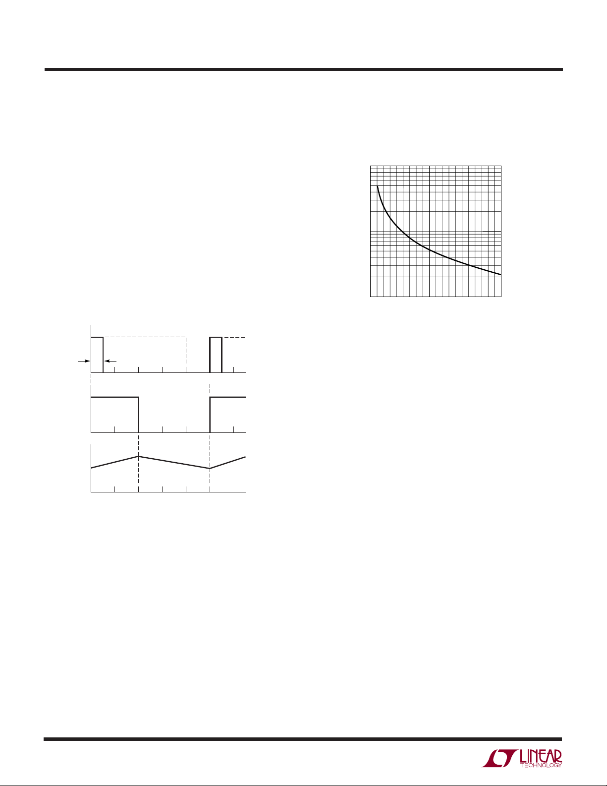
Programming the Operating Frequency
The choice of operating frequency and inductor value is a
tradeoff between efficiency and component size. Low
frequency operation improves efficiency by reducing
MOSFET and diode switching losses. However, lower
frequency operation requires more inductance for a given
amount of load current.
The LTC1871 uses a constant frequency architecture that
can be programmed over a 50kHz to 1000kHz range with
a single external resistor from the FREQ pin to ground, as
shown in Figure 1. The nominal voltage on the FREQ pin is
0.6V, and the current that flows into the FREQ pin is used
to charge and discharge an internal oscillator capacitor. A
graph for selecting the value of R
for a given operating
T
frequency is shown in Figure 6.
1000
100
(kΩ)
T
R
INTV
10
Regulator Bypassing and Operation
CC
200 1000
100
0
Figure 6. Timing Resistor (RT) Value
400
500
300
FREQUENCY (kHz)
800700600
900
1871 F06
An internal, P-channel low dropout voltage regulator produces the 5.2V supply which powers the gate driver and
logic circuitry within the LTC1871, as shown in Figure 7.
The INTV
regulator can supply up to 50mA and must be
CC
bypassed to ground immediately adjacent to the IC pins
with a minimum of 4.7µF tantalum or ceramic capacitor.
Good bypassing is necessary to supply the high transient
currents required by the MOSFET gate driver.
For input voltages that don’t exceed 7V (the absolute
maximum rating for this pin), the internal low dropout
regulator in the LTC1871 is redundant and the INTV
can be shorted directly to the V
pin. With the INTVCC pin
IN
CC
pin
shorted to VIN, however, the divider that programs the
regulated INTV
voltage will draw 10µA of current from
CC
the input supply, even in shutdown mode. For applications
that require the lowest shutdown mode input supply
current, do not connect the INTVCC pin to VIN. Regardless
of whether the INTV
pin is shorted to VIN or not, it is
CC
always necessary to have the driver circuitry bypassed
with a 4.7µF tantalum or low ESR ceramic capacitor to
ground immediately adjacent to the INTVCC and GND
pins.
In an actual application, most of the IC supply current is
used to drive the gate capacitance of the power MOSFET.
1871fc
10
WUUU
APPLICATIO S I FOR ATIO
LTC1871
1.230V
R2
–
DRIVER
P-CH
5.2V
INTV
+
R1
LOGIC
Figure 7. Bypassing the LDO Regulator and Gate Driver Supply
As a result, high input voltage applications in which a large
power MOSFET is being driven at high frequencies can
cause the LTC1871 to exceed its maximum junction
temperature rating. The junction temperature can be
estimated using the following equations:
I
≈ IQ + f • Q
Q(TOT)
G
PIC = VIN • (IQ + f • QG)
= TA + PIC • R
T
J
The total quiescent current I
supply current (I
TH(JA)
consists of the static
Q(TOT)
) and the current required to charge and
Q
discharge the gate of the power MOSFET. The 10-pin
MSOP package has a thermal resistance of R
TH(JA)
=
120°C/W.
As an example, consider a power supply with V
V
= 12V at IO = 1A. The switching frequency is 500kHz,
O
= 5V and
IN
and the maximum ambient temperature is 70°C. The
power MOSFET chosen is the IRF7805, which has a
maximum R
of 11mΩ (at room temperature) and a
DS(ON)
maximum total gate charge of 37nC (the temperature
coefficient of the gate charge is low).
= 600µA + 37nC • 500kHz = 19.1mA
I
Q(TOT)
P
= 5V • 19.1mA = 95mW
IC
= 70°C + 120°C/W • 95mW = 81.4°C
T
J
V
GATE
GND
IN
C
IN
CC
+
C
VCC
4.7µF
PLACE AS CLOSE AS
1871 F07
POSSIBLE TO DEVICE PINS
INPUT
SUPPLY
2.5V TO 30V
M1
GND
This demonstrates how significant the gate charge current
can be when compared to the static quiescent current in
the IC.
To prevent the maximum junction temperature from being
exceeded, the input supply current must be checked when
operating in a continuous mode at high V
. A tradeoff
IN
between the operating frequency and the size of the power
MOSFET may need to be made in order to maintain a
reliable IC junction temperature. Prior to lowering the
operating frequency, however, be sure to check with
power MOSFET manufacturers for their latest-and-greatest low QG, low R
devices. Power MOSFET manu-
DS(ON)
facturing technologies are continually improving, with
newer and better performance devices being introduced
almost yearly.
Output Voltage Programming
The output voltage is set by a resistor divider according to
the following formula:
R
2
VV
=+
1 230 1
.•
O
⎛
⎜
⎝
⎞
⎟
⎠
R
1
The external resistor divider is connected to the output as
shown in Figure 1, allowing remote voltage sensing. The
resistors R1 and R2 are typically chosen so that the error
1871fc
11
 Loading...