

400ksps, Low Power, Sampling ADCs
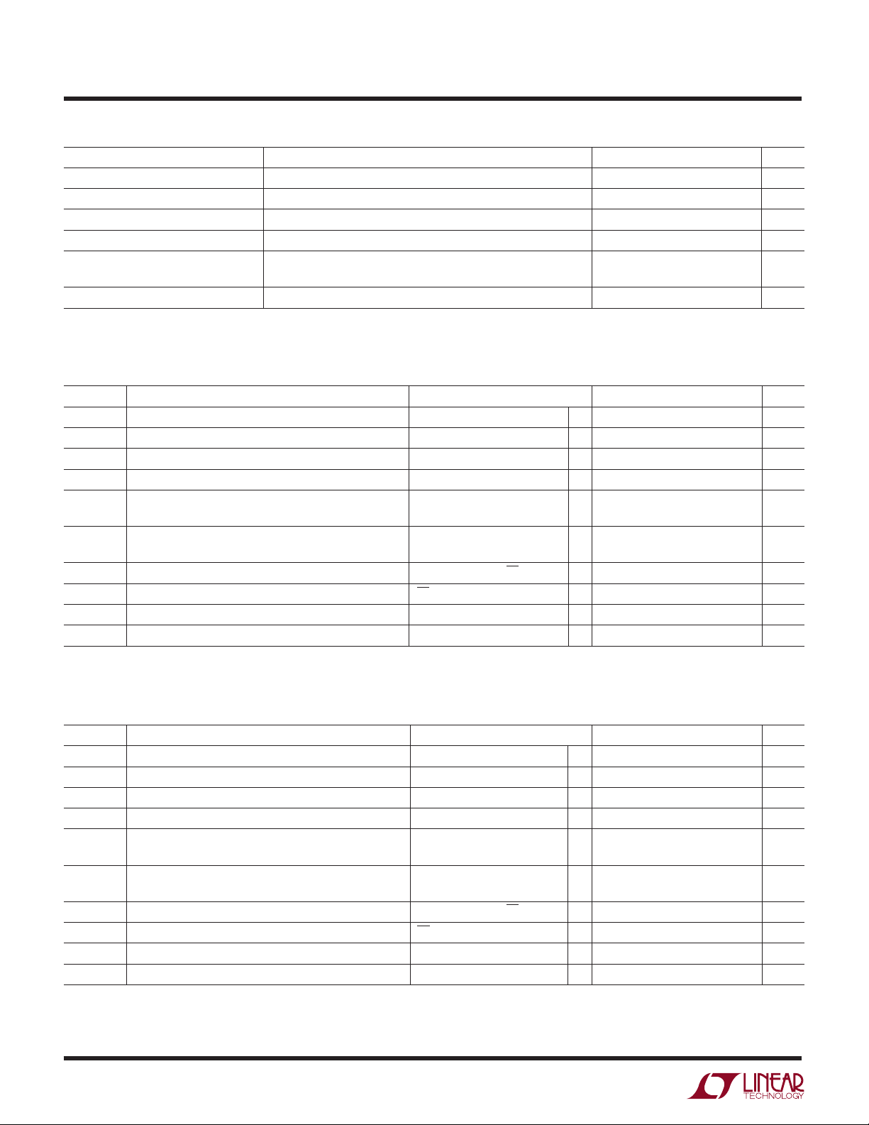
0 512 1024 1536 2048 2560 3072 3584 4096
CODE
1.0
0.5
0
–0.5
–1.0
INL ERROR (LSBs)
1852 F01
FEATURES
■
Flexible 8-Channel Multiplexer
Single-Ended or Differential Inputs
Two Gain Ranges
Unipolar or Bipolar Operation
■
Scan Mode and Programmable Sequencer
Eliminate Configuration Software Overhead
■
Low Power: 3mW at 250ksps
■
2.7V to 5.5V Supply Range
■
Internal or External Reference Operation
■
Parallel Output Includes MUX Address
■
Nap and Sleep Shutdown Modes
■
Pin Compatible up-grade 1.25Msps 10-Bit LTC1850
and 12-Bit LTC1851
U
APPLICATIO S
■
High Speed Data Acquisition
■
Test and Measurement
■
Imaging Systems
■
Telecommunications
■
Industrial Process Control
■
Spectrum Analysis
LTC1852/LTC1853
8-Channel, 10-Bit/12-Bit,
U
DESCRIPTIO
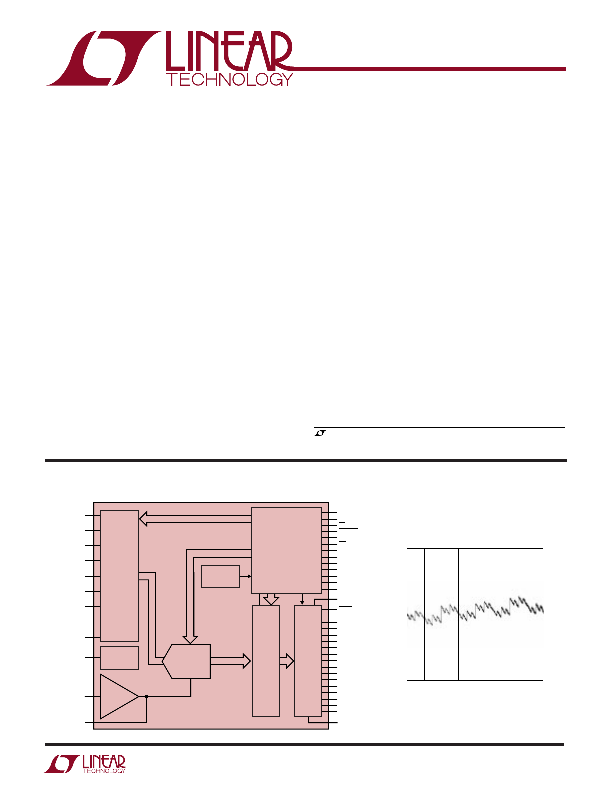
The 10-bit LTC®1852 and 12-bit LTC1853 are complete
8-channel data acquisition systems. They include a flexible 8-channel multiplexer, a 400ksps successive approximation analog-to-digital converter, an internal reference
and a parallel output interface. The multiplexer can be
configured for single-ended or differential inputs, two gain
ranges and unipolar or bipolar operation. The ADCs have
a scan mode that will repeatedly cycle through all 8
multiplexer channels and can also be programmed to
sequence through up to 16 addresses and configurations.
The sequence can also be read back from internal memory.
The reference and buffer amplifier provide pin strappable
ranges of 4.096V, 2.5V and 2.048V. The parallel output
includes the 10-bit or 12-bit conversion result plus the 4bit multiplexer address. The digital outputs are powered
from a separate supply allowing for easy interface to 3V
digital logic. Typical power consumption is 10mW at
400ksps from a single 5V supply and 3mW at 250ksps
from a single 3V supply.
, LTC and LT are registered trademarks of Linear Technology Corporation.
BLOCK DIAGRA
CH0
CH1
CH2
CH3
CH4
CH5
CH6
CH7
COM
REFOUT
REFIN
REFCOMP
8-CHANNEL
MULTIPLEXER
2.5V
REFERENCE
REF AMP
+
–
W
LTC1853
12-BIT
SAMPLING
ADC
INTERNAL
CLOCK
CONTROL LOGIC
PROGRAMMABLE
SEQUENCER
DATA
LATCHES
AND
OUTPUT
DRIVERS
18523 BD
M1
SHDN
CS
CONVST
RD
WR
DIFF
A2
A1
A0
UNI/BIP
PGA
M0
OV
DD
BUSY
DIFF
OUT
A2
OUT
A1
OUT
A0
OUT
D11/S2
D10/S1
D9/S0
D8
D7
D6
D5
D4
D3
D2
D1
D0
OGND
Integral Linearity
/S6
/S5
/S4
/S3
18523f
1
LTC1852/LTC1853
A
S
OVDD = V
W
O
LUTEXI TIS
(Notes 1, 2)
DD
A
WUW
U
ARB
G
Supply Voltage (VDD)................................................. 6V
Analog Input Voltage (Note 3) ..... –0.3V to (VDD + 0.3V)
Digital Input Voltage (Note 4) ....................–0.3V to 10V
Digital Output Voltage..................–0.3V to (VDD + 0.3V)
Power Dissipation.............................................. 500mW
WU
/
PACKAGE
CH0
CH1
CH2
CH3
CH4
CH5
CH6
CH7
COM
REFOUT
REFIN
REFCOMP
GND
V
DD
V
DD
GND
/S6
DIFF
OUT
/S5
A2
OUT
/S4
A1
OUT
/S3
A0
OUT
D9/S2
D8/S1
D7/S0
D6
T
O
RDER I FOR ATIO
TOP VIEW
1
2
3
4
5
6
7
8
9
10
11
12
13
14
15
16
17
18
19
20
21
22
23
24
FW PACKAGE
48-LEAD PLASTIC TSSOP
= 150°C, θJA = 110°C/W
JMAX
48
47
46
45
44
43
42
41
40
39
38
37
36
35
34
33
32
31
30
29
28
27
26
25
M1
SHDN
CS
CONVST
RD
WR
DIFF
A2
A1
A0
UNI/BIP
PGA
M0
OV
DD
OGND
BUSY
NC
NC
D0
D1
D2
D3
D4
D5
ORDER PART
NUMBER
LTC1852CFW
LTC1852IFW
Ambient Operating Temperature Range
LTC1852C/LTC1853C ............................ 0°C to 70°C
LTC1852I/LTC1853I .......................... –40°C to 85°C
Storage Temperature Range .................–65°C to 150°C
Lead Temperature (Soldering, 10 sec)................ 300°C
U
REFOUT
REFIN
REFCOMP
DIFF
OUT
A2
OUT
A1
OUT
A0
OUT
D11/S2
D10/S1
D9/S0
1
CH0
2
CH1
3
CH2
4
CH3
5
CH4
6
CH5
7
CH6
8
CH7
9
COM
10
11
12
13
GND
14
V
DD
15
V
DD
16
GND
17
/S6
18
/S5
19
/S4
20
/S3
21
22
23
24
D8
FW PACKAGE
48-LEAD PLASTIC TSSOP
T
= 150°C, θJA = 110°C/W
JMAX
TOP VIEW
48
47
46
45
44
43
42
41
40
39
38
37
36
35
34
33
32
31
30
29
28
27
26
25
M1
SHDN
CS
CONVST
RD
WR
DIFF
A2
A1
A0
UNI/BIP
PGA
M0
OV
DD
OGND
BUSY
D0
D1
D2
D3
D4
D5
D6
D7
ORDER PART
NUMBER
LTC1853CFW
LTC1853IFW
Consult LTC Marketing for parts specified with wider operating temperature ranges.
2
18523f
LTC1852/LTC1853
U
CO VERTER CHARACTERISTICS
temperature range, otherwise specifications are at TA = 25°C. VDD = 2.7V to 5.5V, REFCOMP < VDD (Notes 5, 6)
PARAMETER CONDITIONS MIN TYP MAX MIN TYP MAX UNITS
Resolution (No Missing Codes) ● 10 12 Bits
Integral Linearity Error (Note 7) ● ±0.25 ±1 ±0.35 ±1LSB
Differential Linearity Error ● ±0.25 ±1 ±0.25 ±1LSB
Offset Error (Bipolar and Unipolar) (Note 8)
Gain = 1 (PGA = 1) REFCOMP ≥ 2V
Gain = 2 (PGA = 0)
Offset Error Match (Bipolar and Unipolar) ±0.5 ±1LSB
Unipolar Gain Error With External 4.096V Reference
Gain = 1 (PGA = 1) Applied to REFCOMP (Note 12) ±2 ±4LSB
Gain = 2 (PGA = 0) V
Unipolar Gain Error Match ±0.5 ±1LSB
Bipolar Gain Error With External 4.096V Reference
Gain = 1 (PGA = 1) Applied to REFCOMP (Note 12) ±2 ±4LSB
Gain = 2 (PGA = 0) V
Bipolar Gain Error Match ±0.5 ±1LSB
Unipolar Gain Error With External 2.5V Reference
Gain = 1 (PGA = 1) Applied to REFCOMP ● ±1 ±3 ±1.5 ±8LSB
Gain = 2 (PGA = 0) V
Bipolar Gain Error With External 2.5V Reference
Gain = 1 (PGA = 1) Applied to REFCOMP ● ±1 ±3 ±1.5 ±8LSB
Gain = 2 (PGA = 0) V
Full-Scale Error Temperature Coefficient 15 15 ppm/°C
= 4.75V to 5.25V, fS ≤ 400kHz ±4 ±8LSB
DD
= 4.75V to 5.25V, fS ≤ 400kHz ±4 ±8LSB
DD
= 2.7V to 5.5V, fS ≤ 250kHz ● ±2 ±6 ±3 ±16 LSB
DD
= 2.7V to 5.5V, fS ≤ 250kHz ● ±2 ±6 ±3 ±16 LSB
DD
The ● denotes the specifications which apply over the full operating
LTC1852 LTC1853
● ±0.5 ±2 ±1 ±6LSB
● ±1 ±4 ±2 ±12 LSB
UU
A ALOG I PUT
specifications are at TA = 25°C. (Note 5)
SYMBOL PARAMETER CONDITIONS MIN TYP MAX UNITS
V
IN
I
IN
C
IN
t
ACQ
t
S(MUX)
t
AP
t
jitter
CMRR Analog Input Common Mode Rejection Ratio 60 dB
Analog Input Range (Note 9) 2.7V ≤ VDD ≤ 5.5V, REFCOMP ≤ V
Unipolar, Gain = 1 (PGA = 1) 0 – REFCOMP V
Unipolar, Gain = 2 (PGA = 0) 0 – REFCOMP/2 V
Bipolar, Gain = 1 (PGA = 1) ±REFCOMP/2 V
Bipolar, Gain = 2 (PGA = 0) ±REFCOMP/4 V
Analog Input Leakage Current ● ±1 µA
Analog Input Capacitance Between Conversions (Gain = 1) 15 pF
Sample-and-Hold Acquisition Time 50 150 ns
Multiplexer Settling Time (Includes t
Sample-and-Hold Aperture Delay Time VDD = 5V –0.5 ns
Sample-and-Hold Aperture Delay Time Jitter VDD = 5V 2 ps
U
W
DY A IC ACCURACY
SYMBOL PARAMETER CONDITIONS MIN TYP MAX UNITS
S/(N + D) Signal-to-Noise Plus Distortion Ratio 40kHz Input Signal 72.5 dB
THD Total Harmonic Distortion 40kHz Input Signal, First 5 Harmonics –80 dB
SFDR Spurious Free Dynamic Range 40kHz Input Signal –85 dB
The ● denotes the specifications which apply over the full operating temperature range, otherwise
DD
Between Conversions (Gain = 2) 25 pF
During Conversions 5 pF
) 50 150 ns
ACQ
TA = 25°C. (Note 5)
18523f
RMS
3
LTC1852/LTC1853
UU U
I TER AL REFERE CE
PARAMETER CONDITIONS MIN TYP MAX UNITS
REFOUT Output Voltage I
REFOUT Output Temperature Coefficient I
REFOUT Line Regulation 2.7 ≤ VDD ≤ 5.5, I
Reference Buffer Gain 1.6368 1.6384 1.6400 V/V
REFCOMP Output Voltage External 2.5V Reference (VDD = 5V) 4.092 4.096 4.100 V
REFCOMP Impedance Impedance to GND, REFIN = V
TA = 25°C. (Notes 5, 6)
= 0 2.48 2.50 2.52 V
OUT
= 0 ±15 ppm/°C
OUT
= 0 0.01 LSB/V
OUT
Internal 2.5V Reference (V
= 5V) 4.060 4.096 4.132 V
DD
DD
19.2 kΩ
UU
DIGITAL I PUTS A D DIGITAL OUTPUTS
full operating temperature range, otherwise specifications are at TA = 25°C. VDD = 5V (Note 5)
SYMBOL PARAMETER CONDITIONS MIN TYP MAX UNITS
V
IH
V
IL
I
IN
C
IN
V
OH
V
OL
I
OZ
C
OZ
I
SOURCE
I
SINK
High Level Input Voltage VDD = 5.25V ● 2.4 V
Low Level Input Voltage VDD = 4.75V ● 0.8 V
Digital Input Current VIN = 0V to V
Digital Input Capacitance 1.5 pF
High Level Output Voltage VDD = 4.75V, IO = –10µA 4.5 V
= 4.75V, IO = –200µA ● 4V
V
DD
Low Level Output Voltage VDD = 4.75V, IO = 160µA 0.05 V
= 4.75V, IO = 1.6mA ● 0.10 0.4 V
V
DD
Hi-Z Output Leakage D11 to D0, A0, A1, A2
Hi-Z Capacitance D11 to D0 CS High (Note 9) ● 15 pF
Output Source Current V
Output Sink Current V
OUT
, DIFF
OUTVOUT
OUT
OUT
= 0V to VDD, CS High ● ±10 µA
= 0V –20 mA
= V
The ● denotes the specifications which apply over the
DD
DD
● ±5 µA
30 mA
UU
DIGITAL I PUTS A D DIGITAL OUTPUTS
full operating temperature range, otherwise specifications are at TA = 25°C. VDD = 3V (Note 5)
SYMBOL PARAMETER CONDITIONS MIN TYP MAX UNITS
V
IH
V
IL
I
IN
C
IN
V
OH
V
OL
I
OZ
C
OZ
I
SOURCE
I
SINK
High Level Input Voltage VDD = 3.3V ● 1.9 V
Low Level Input Voltage VDD = 2.7V ● 0.45 V
Digital Input Current VIN = 0V to V
Digital Input Capacitance 1.5 pF
High Level Output Voltage VDD = 2.7V, IO = –10µA 2.5 V
= 2.7V, IO = –200µA ● 2V
V
DD
Low Level Output Voltage VDD = 2.7V, IO = 160µA 0.05 V
= 2.7V, IO = 1.6mA ● 0.10 0.4 V
V
DD
Hi-Z Output Leakage D11 to D0, A0, A1, A2
Hi-Z Capacitance D11 to D0 CS High (Note 9) ● 15 pF
Output Source Current V
Output Sink Current V
OUT
, DIFF
OUTVOUT
OUT
OUT
= 0V to VDD, CS High ● ±10 µA
= 0V –10 mA
= V
The ● denotes the specifications which apply over the
DD
DD
● ±5 µA
15 mA
18523f
4
LTC1852/LTC1853
WU
POWER REQUIRE E TS
range, otherwise specifications are at TA = 25°C. (Note 5)
SYMBOL PARAMETER CONDITIONS MIN TYP MAX UNITS
V
DD
OV
I
DD
P
DISS
I
DDPD
DD
Analog Positive Supply Voltage (Note 10) ● 2.7 5.5 V
Output Positive Supply Voltage (Note 10) ● 2.7 5.5 V
Positive Supply Current VDD = OVDD = 5V, fS = 400kHz ● 23mA
Power Dissipation VDD = OVDD = 5V, fS = 400kHz ● 10 15 mW
Power Down Positive Supply Current
Nap Mode SHDN = Low, CS = Low 0.5 mA
Sleep Mode SHDN = Low, CS = High 20 µA
Power Down Power Dissipation VDD = VDD = OVDD = 5V, fS = 400kHz
Nap Mode SHDN = Low, CS = Low 2.5 mW
Sleep Mode SHDN = Low, CS = High 0.1 mW
Power Down Power Dissipation VDD = VDD = OVDD = 3V, fS = 250kHz
Nap Mode SHDN = Low, CS = Low 1.5 mW
Sleep Mode SHDN = Low, CS = High 0.06 mW
The ● denotes the specifications which apply over the full operating temperature
V
= OVDD = 2.7V, fS = 250kHz ● 0.83 1.33 mA
DD
V
= OVDD = 2.7V, fS = 250kHz ● 2.25 4 mW
DD
UW
TI I G CHARACTERISTICS
range, otherwise specifications are at TA = 25°C. (Note 5)
The ● denotes the specifications which apply over the full operating temperature
SYMBOL PARAMETER CONDITIONS MIN TYP MAX UNITS
f
SAMPLE(MAX)
t
CONV
t
ACQ
t
1
t
2
t
3
t
4
t
5
t
6
t
7
t
8
t
9
t
10
t
11
Maximum Sampling Frequency VDD = 5.5V ● 400 kHz
V
= 2.7V ● 250 kHz
DD
Acquisition + Conversion VDD = 5.5V ● 2.5 µs
VDD = 2.7V ● 4.0 µs
Conversion Time VDD = 5.5V ● 2.0 µs
VDD = 2.7V ● 3.5 µs
Acquisition Time (Note 13) ● 150 ns
CS to RD Setup Time (Notes 9, 10) ● 0ns
CS to CONVST Setup Time (Notes 9, 10) ● 10 ns
CS to SHDN Setup Time (Notes 9, 10) 200 ns
SHDN to CONVST Wake-Up Time Nap Mode (Note 10) 200 ns
Sleep Mode (Note 10) 10 ms
CONVST Low Time (Notes 10, 11) ● 50 ns
CONVST to BUSY Delay CL = 25pF 10 ns
● 60 ns
Data Ready Before BUSY 20 35 ns
● 15 ns
Delay Between Conversions (Note 10) ● 50 ns
Wait Time RD After BUSY ● –5 ns
Data Access Time After RD CL = 25pF 20 35 ns
● 45 ns
CL = 100pF 25 45 ns
● 60 ns
BUS Relinquish Time 10 30 ns
0°C to 70°C
–40°C to 85°C ● 40 ns
● 35 ns
18523f
5
LTC1852/LTC1853
UW
TI I G CHARACTERISTICS
range, otherwise specifications are at TA = 25°C. (Note 5)
SYMBOL PARAMETER CONDITIONS MIN TYP MAX UNITS
t
12
t
13
t
14
t
15
t
16
t
17
t
18
t
19
t
20
t
21
t
22
t
23
t
24
t
25
t
26
t
27
Note 1: Absolute maximum ratings are those values beyond which the life
of a device may be impaired.
Note 2: All voltage values are with respect to ground with OGND and GND
wired together unless otherwise noted.
Note 3: When these pin voltages are taken below ground or above VDD,
they will be clamped by internal diodes. This product can handle input
currents of 100mA below ground or above V
Note 4: When these pin voltages are taken below ground, they will be
clamped by internal diodes. This product can handle input currents of
100mA below ground without latchup. These pins are not clamped to VDD.
Note 5: V
specified.
Note 6: Linearity, offset and full-scale specifications apply for a singleended input on any channel with COM grounded.
Note 7: Integral nonlinearity is defined as the deviation of a code from a
straight line passing through the actual end points of the transfer curve.
The deviation is measured from the center of the quantization band.
RD Low Time ● t
CONVST High Time (Note 10) ● 50 ns
Latch Setup Time (Note 10) ● 10 ns
Latch Hold Time (Notes 9, 10) ● 10 ns
WR Low Time (Note 10) ● 50 ns
WR High Time (Note 10) ● 50 ns
M1 to M0 Setup Time (Notes 9, 10) ● 10 ns
M0 to BUSY Delay M1 High 20 ns
M0 to WR (or RD) Setup Time (Notes 9, 10) ● t
M0 High Pulse Width (Note 10) ● 50 ns
RD High Time Between Readback Reads (Note 10) ● 50 ns
Last WR (or RD) to M0 (Note 10) ● 10 ns
M0 to RD Setup Time (Notes 9, 10) ● t
M0 to CONVST (Note 10) ● t
Aperture Delay –0.5 ns
Aperture Jitter 2ps
without latchup.
DD
= 5V, f
DD
= 400kHz, tr = tf = 2ns unless otherwise
SAMPLE
The ● denotes the specifications which apply over the full operating temperature
10
19
19
19
Note 8: Bipolar offset is the offset voltage measured from –0.5LSB when
the output code flickers between 1111 1111 1111 and 0000 0000 0000.
For the LTC1853 and between 11 1111 1111 and 00 0000 0000 for the
LTC1852.
Note 9: Guaranteed by design, not subject to test.
Note 10: Recommended operating conditions.
Note 11: The falling CONVST edge starts a conversion. If CONVST returns
high at a critical point during the conversion it can create small errors. For
the best results, ensure that CONVST returns high either within 400ns
after the start of the conversion or after BUSY rises.
Note 12: The analog input range is determined by the voltage on
REFCOMP. The gain error specification is tested with an external 4.096V
but is valid for any value of REFCOMP greater than 2V and less than
– 0.5V.)
(V
DD
Note 13: MUX address is updated immediately after BUSY falls.
ns
ns
ns
ns
RMS
UW
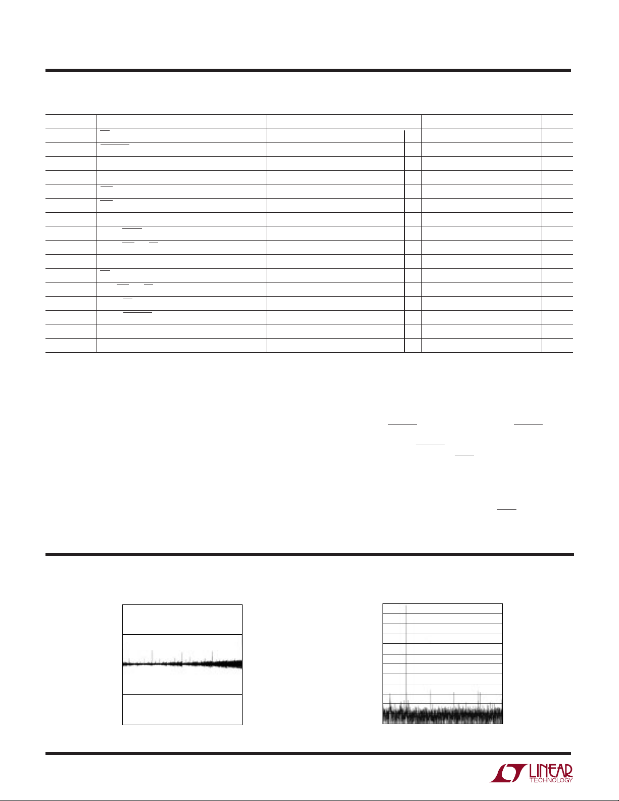
TYPICAL PERFOR A CE CHARACTERISTICS
Differential Linearity
1.0
0.5
0
DNL ERROR (LBS)
–0.5
–1.0
0 4096
CODE
1852 F02
6
8192 Point FFT with
fIN = 39.599kHz
0
–20
–40
–60
–80
AMPLITUDE (dB)
–100
–120
0200
FREQUENCY (kHz)
1852 F03
18523f

LTC1852/LTC1853
U
UU
PI FU CTIO S
CH0 to CH7 (Pins 1 to 8): Analog Input Pins. Input pins can
be used single ended relative to the analog input common
pin or differentially in pairs (CH0 and CH1, CH2 and CH3,
CH4 and CH5, CH6 and CH7).
COM (Pin 9): Analog Input Common Pin. For single-ended
operation (DIFF = 0), COM is the “–” analog input. COM is
disabled when DIFF is high.
REFOUT (Pin 10): Internal 2.5V Reference Output. Bypass
to analog ground plane with 1µF.
REFIN (Pin 11): Reference Mode Select/Reference Buffer
Input. REFIN selects the reference mode and acts as the
reference buffer input. REFIN tied to ground (Logic 0) will
produce 2.048V on the REFCOMP pin. REFIN tied to the
positive supply (Logic 1) disables the reference buffer to
allow REFCOMP to be driven externally. For voltages
between 1V and 2.6V, the reference buffer produces an
output voltage on the REFCOMP pin equal to 1.6384 times
the voltage on REFIN (4.096V on REFCOMP for a 2.5V
input on REFIN).
REFCOMP (Pin 12): Reference Buffer Output. REFCOMP
sets the full-scale input span. The reference buffer produces an output voltage on the REFCOMP pin equal to
1.6384 times the voltage on the REFIN pin (4.096V on
REFCOMP for a 2.5V input on REFIN). REFIN tied to
ground will produce 2.048V on the REFCOMP pin.
REFCOMP can be driven externally if REFIN is tied to the
positive supply. Bypass to analog ground plane with 10µF
tantalum in parallel with 0.1µF ceramic or 10µF ceramic.
GND (Pins 13, 16): Ground. Tie to analog ground plane.
VDD (Pins 14, 15): Positive Supply. Bypass to analog
ground plane with 10µF tantalum in parallel with 0.1µF
ceramic or 10µF ceramic.
DIFF
Active when RD is low. Following a conversion, the singleended/differential bit of the present conversion is available
on this pin concurrent with the conversion result. In
Readback mode, the single-ended/differential bit of the
current sequencer location (S6) is available on this pin.
The output swings between OVDD and OGND.
/S6 (Pin 17): Three-State Digital Data Output.
OUT
A2
/S5, A1
OUT
State Digital MUX Address Outputs. Active when RD is
low. Following a conversion, the MUX address of the
present conversion is available on these pins concurrent
with the conversion result. In Readback mode, the MUX
address of the current sequencer location (S5-S3) is
available on these pins. The outputs swing between OV
and OGND.
D9/S2 (Pin 21, LTC1852): Three-State Digital Data Output. Active when RD is low. Following a conversion, bit 9
of the present conversion is available on this pin. In
Readback mode, the unipolar/bipolar bit of the current
sequencer location (S2) is available on this pin. The output
swings between OVDD and OGND.
D11/S2 (Pin 21, LTC1853): Three-State Digital Data Output. Active when RD is low. Following a conversion, bit 11
of the present conversion is available on this pin. In
Readback mode, the unipolar/bipolar bit of the current
sequencer location (S2) is available on this pin. The output
swings between OVDD and OGND.
D8/S1 (Pin 22, LTC1852): Three-State Digital Data Outputs. Active when RD is low. Following a conversion, bit 8
of the present conversion is available on this pin. In
Readback mode, the gain bit of the current sequencer
location (S1) is available on this pin. The output swings
between OVDD and OGND.
D10/S1 (Pin 22, LTC1853): Three-State Digital Data Outputs. Active when RD is low. Following a conversion, bit 10
of the present conversion is available on this pin. In
Readback mode, the gain bit of the current sequencer
location (S1) is available on this pin. The output swings
between OVDD and OGND.
D7/S0 (Pin 23, LTC1852): Three-State Digital Data Outputs. Active when RD is low. Following a conversion, bit 7
of the present conversion is available on this pin. In
Readback mode, the end of sequence bit of the current
sequencer location (S0) is available on this pin. The output
swings between OVDD and OGND.
OUT
/S4, A0
/S3 (Pins 18 to 20): Three-
OUT
DD
18523f
7

LTC1852/LTC1853
U
UU
PI FU CTIO S
D9/S0 (Pin 23, LTC1853): Three-State Digital Data Outputs. Active when RD is low. Following a conversion, bit 9
of the present conversion is available on this pin. In
Readback mode, the end of sequence bit of the current
sequencer location (S0) is available on this pin. The output
swings between OVDD and OGND.
D6 to D0 (Pins 24 to 30, LTC1852): Three-State Digital
Data Outputs. Active when RD is low. The outputs swing
between OVDD and OGND.
D8 to D0 (Pins 24 to 32, LTC1853): Three-State Digital
Data Outputs. Active when RD is low. The outputs swing
between OVDD and OGND.
NC (Pins 31 to 32, LTC1852): No Connect. There is no
internal connection to these pins.
BUSY (Pin 33): Converter Busy Output. The BUSY output
has two functions. At the start of a conversion, BUSY will
go low and remain low until the conversion is completed.
The rising edge may be used to latch the output data. BUSY
will also go low while the part is in Program/Readback
mode (M1 high, M0 low) and remain low until M0 is brought
back high. The output swings between OVDD and OGND.
OGND (Pin 34): Digital Data Output Ground. Tie to analog
ground plane. May be tied to logic ground if desired.
A0 to A2 (Pins 39 to 41): MUX Address Input Pins.
DIFF (Pin 42): Single-Ended/Differential Select Input. A
low logic level selects single ended, a high logic level
selects differential.
WR (Pin 43): Write Input. In Direct Address mode, WR low
enables the MUX address and configuration input pins
(Pins 37 to 42). WR can be tied low or the rising edge of
WR can be used to latch the data. In Program mode, WR
is used to program the sequencer. WR low enables the
MUX address and configuration input pins (Pins 37 to 42).
The rising edge of WR latches the data and increments the
counter to the next sequencer location.
RD (Pin 44): Read Input. During normal operation, RD
enables the output drivers when CS is low. In Readback
mode (M1 high, M0 low), RD going low reads the current
sequencer location, RD high advances to the next sequencer location.
CONVST (Pin 45): Conversion Start Input. This active low
signal starts a conversion on its falling edge.
CS (Pin 46): Chip Select Input. The chip select input must
be low for the ADC to recognize the CONVST and RD
inputs. If SHDN is low, a low logic level on CS selects Nap
mode; a high logic level on CS selects Sleep mode.
OVDD (Pin 35): Digital Data Output Supply. Normally tied
to 5V, can be used to interface with 3V digital logic. Bypass
to OGND with 10µF tantalum in parallel with 0.1µF ceramic
or 10µF ceramic.
M0 (Pin 36): Mode Select Pin 0. Used in conjunction with
M1 to select operating mode. See Table 5.
PGA (Pin 37): Gain Select Input. A high logic level selects
gain = 1, a low logic level selects gain = 2.
UNI/BIP (Pin 38): Unipolar/Bipolar Select Input. Logic low
selects a unipolar input span, a high logic level selects a
bipolar input span.
SHDN (Pin 47): Power Shutdown Input. A low logic level
will invoke the Shutdown mode selected by the CS pin. CS
low selects Nap mode, CS high selects Sleep mode. Tie
high if unused.
M1 (Pin 48): Mode Select Pin 1. Used in conjunction with
M0 to select operating mode. See Table 5.
18523f
8
 Loading...