

FEATURES
No R
DESCRIPTIO
SENSE
LTC1778/LTC1778-1
Wide Operating Range,
TM
Step-Down Controller
U
■
No Sense Resistor Required
■
True Current Mode Control
■
Optimized for High Step-Down Ratios
■
t
ON(MIN)
■
Extremely Fast Transient Response
■
Stable with Ceramic C
■
Dual N-Channel MOSFET Synchronous Drive
■
Power Good Output Voltage Monitor (LTC1778)
■
Adjustable On-Time (LTC1778-1)
■
Wide VIN Range: 4V to 36V
■
±1% 0.8V Voltage Reference
■
Adjustable Current Limit
■
Adjustable Switching Frequency
■
Programmable Soft-Start
■
Output Overvoltage Protection
■
Optional Short-Circuit Shutdown Timer
■
Micropower Shutdown: IQ < 30µA
■
Available in a 16-Pin Narrow SSOP Package
≤ 100ns
OUT
U
APPLICATIO S
■
Notebook and Palmtop Computers
■
Distributed Power Systems
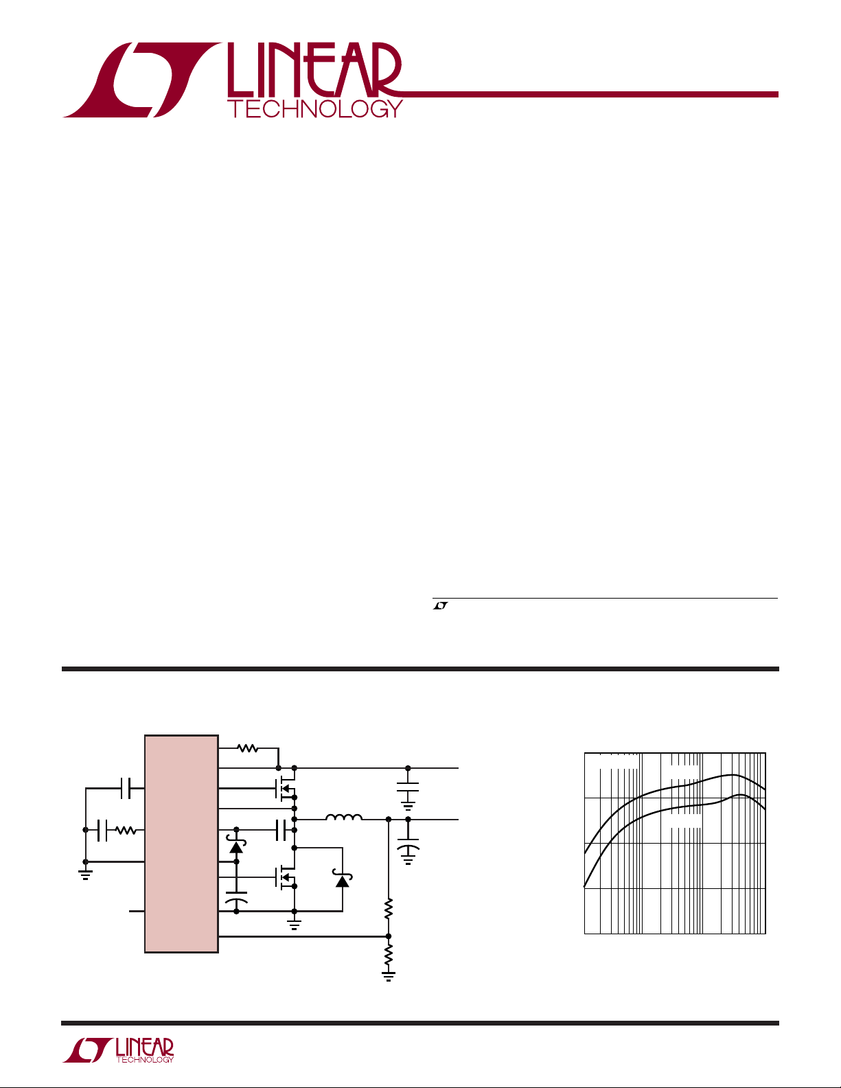
The LTC®1778 is a synchronous step-down switching
regulator controller optimized for CPU power. The controller uses a valley current control architecture to deliver
very low duty cycles with excellent transient response
without requiring a sense resistor. Operating frequency is
selected by an external resistor and is compensated for
variations in VIN.
Discontinuous mode operation provides high efficiency
operation at light loads. A forced continuous control pin
reduces noise and RF interference, and can assist secondary winding regulation by disabling discontinuous operation when the main output is lightly loaded.
Fault protection is provided by internal foldback current
limiting, an output overvoltage comparator and optional
short-circuit shutdown timer. Soft-start capability for supply sequencing is accomplished using an external timing
capacitor. The regulator current limit level is user programmable. Wide supply range allows operation from 4V to 36V
at the input and from 0.8V up to (0.9)VIN at the output.
, LTC and LT are registered trademarks of Linear Technology Corporation.
No R
All other trademarks are the property of their respective owners.
Protected by U.S. Patents, including 5481178, 6100678, 6580258, 5847554, 6304066
is a trademark of Linear Technology Corporation.
SENSE
TYPICAL APPLICATIO
R
ON
1.4MΩ
I
BOOST
LTC1778
INTV
V
SW
BG
PGND
V
ON
IN
TG
CB 0.22µF
D
B
CMDSH-3
CC
+
C
4.7µF
FB
C
C
500pF
C
SS
0.1µF
RUN/SS
I
TH
R
C
20k
SGND
PGOOD
Figure 1. High Efficiency Step-Down Converter
VCC
U
M1
Si4884
M2
Si4874
L1
1.8µH
D1
B340A
+
R2
30.1k
R1
14k
1778 F01a
C
IN
10µF
50V
×3
C
OUT
180µF
4V
×2
V
IN
5V TO 28V
V
OUT
2.5V
10A
Efficiency vs Load Current
100
V
OUT
90
80
EFFICIENCY (%)
70
60
0.01
= 2.5V
0.1
LOAD CURRENT (A)
VIN = 5V
VIN = 25V
1
10
1778 F01b
1778fb
1
LTC1778/LTC1778-1
TOP VIEW
GN PACKAGE
16-LEAD PLASTIC SSOP
1
2
3
4
5
6
7
8
16
15
14
13
12
11
10
9
RUN/SS
V
ON
V
RNG
FCB
I
TH
SGND
I
ON
V
FB
BOOST
TG
SW
PGND
BG
INTV
CC
V
IN
EXTV
CC
WWWU
ABSOLUTE AXI U RATI GS
(Note 1)
Input Supply Voltage (VIN, ION)................. 36V to –0.3V
Boosted Topside Driver Supply Voltage
(BOOST) ................................................... 42V to –0.3V
SW Voltage .................................................. 36V to –5V
EXTV
, (BOOST – SW), RUN/SS,
CC
PGOOD Voltages....................................... 7V to – 0.3V
FCB, V
I
TH
, V
ON
Voltages .......... INTVCC + 0.3V to –0.3V
RNG
, VFB Voltages...................................... 2.7V to –0.3V
UU
W
PACKAGE/ORDER I FOR ATIO
RUN/SS
1
2
PGOOD
3
V
RNG
4
FCB
5
I
TH
6
SGND
7
I
ON
8
V
FB
16-LEAD PLASTIC SSOP
T
= 125°C, θJA = 130°C/ W
JMAX
TOP VIEW
GN PACKAGE
BOOST
16
15
TG
14
SW
13
PGND
12
BG
11
INTV
CC
10
V
IN
9
EXTV
CC
ORDER PART
NUMBER
LTC1778EGN
LTC1778IGN
GN PART MARKING
1778
1778I
TG, BG, INTVCC, EXTVCC Peak Currents.................... 2A
TG, BG, INTVCC, EXTVCC RMS Currents .............. 50mA
Operating Ambient Temperature Range (Note 4)
LTC1778E ........................................... – 40°C to 85°C
LTC1778I.......................................... – 40°C to 125°C
Junction Temperature (Note 2)............................ 125°C
Storage Temperature Range ................. –65°C to 150°C
Lead Temperature (Soldering, 10 sec).................. 300°C
ORDER PART
NUMBER
LTC1778EGN-1
GN PART MARKING
17781
T
= 125°C, θJA = 130°C/ W
JMAX
Consult LTC Marketing for parts specified with wider operating temperature ranges.
ELECTRICAL CHARACTERISTICS
The ● denotes specifications which apply over the full operating
temperature range, otherwise specifications are TA = 25°C. VIN = 15V unless otherwise noted.
SYMBOL PARAMETER CONDITIONS MIN TYP MAX UNITS
Main Control Loop
I
Q
V
FB
∆V
FB(LINEREG)
∆V
FB(LOADREG)
I
FB
g
m(EA)
V
FCB
I
FCB
t
ON
t
ON(MIN)
2
Input DC Supply Current
Normal 900 2000 µA
Shutdown Supply Current 15 30 µA
Feedback Reference Voltage ITH = 1.2V (Note 3) LTC1778E ● 0.792 0.800 0.808 V
= 1.2V (Note 3) LTC1778I ● 0.792 0.800 0.812 V
I
TH
Feedback Voltage Line Regulation VIN = 4V to 30V, ITH = 1.2V (Note 3) 0.002 %/V
Feedback Voltage Load Regulation ITH = 0.5V to 1.9V (Note 3) ● –0.05 –0.3 %
Feedback Input Current VFB = 0.8V –5 ±50 nA
Error Amplifier Transconductance ITH = 1.2V (Note 3) ● 1.4 1.7 2 mS
Forced Continuous Threshold ● 0.76 0.8 0.84 V
Forced Continuous Pin Current V
On-Time ION = 30µA, VON = 0V (LTC1778-1) 198 233 268 ns
Minimum On-Time ION = 180µA 50 100 ns
= 0.8V –1 –2 µA
FCB
I
= 15µA, VON = 0V (LTC1778-1) 396 466 536 ns
ON
1778fb
LTC1778/LTC1778-1
ELECTRICAL CHARACTERISTICS
The ● denotes specifications which apply over the full operating
temperature range, otherwise specifications are TA = 25°C. VIN = 15V unless otherwise noted.
SYMBOL PARAMETER CONDITIONS MIN TYP MAX UNITS
t
OFF(MIN)
V
SENSE(MAX)
V
SENSE(MIN)
∆V
FB(OV)
V
FB(UV)
V
RUN/SS(ON)
V
RUN/SS(LE)
V
RUN/SS(LT)
I
RUN/SS(C)
I
RUN/SS(D)
V
IN(UVLO)
V
IN(UVLOR)
TG R
UP
TG R
DOWN
BG R
UP
BG R
DOWN
TG t
r
TG t
f
BG t
r
BG t
f
Internal VCC Regulator
V
INTVCC
∆V
LDO(LOADREG)
V
EXTVCC
∆V
EXTVCC
∆V
EXTVCC(HYS)
PGOOD Output (LTC1778 Only)
∆V
FBH
∆V
FBL
∆V
FB(HYS)
V
PGL
Minimum Off-Time ION = 30µA 250 400 ns
Maximum Current Sense Threshold V
– V
V
PGND
SW
Minimum Current Sense Threshold V
– V
V
PGND
SW
= 1V, VFB = 0.76V ● 113 133 153 mV
RNG
V
= 0V, VFB = 0.76V ● 79 93 107 mV
RNG
V
= INTVCC, VFB = 0.76V ● 158 186 214 mV
RNG
= 1V, VFB = 0.84V – 67 mV
RNG
V
= 0V, VFB = 0.84V – 47 mV
RNG
= INTVCC, VFB = 0.84V – 93 mV
V
RNG
Output Overvoltage Fault Threshold 5.5 7.5 9.5 %
Output Undervoltage Fault Threshold 520 600 680 mV
RUN Pin Start Threshold ● 0.8 1.5 2 V
RUN Pin Latchoff Enable Threshold RUN/SS Pin Rising 4 4.5 V
RUN Pin Latchoff Threshold RUN/SS Pin Falling 3.5 4.2 V
Soft-Start Charge Current V
Soft-Start Discharge Current V
= 0V –0.5 –1.2 –3 µA
RUN/SS
= 4.5V, VFB = 0V 0.8 1.8 3 µA
RUN/SS
Undervoltage Lockout VIN Falling ● 3.4 3.9 V
Undervoltage Lockout Release VIN Rising ● 3.5 4 V
TG Driver Pull-Up On Resistance TG High 2 3 Ω
TG Driver Pull-Down On Resistance TG Low 2 3 Ω
BG Driver Pull-Up On Resistance BG High 3 4 Ω
BG Driver Pull-Down On Resistance BG Low 1 2 Ω
TG Rise Time C
TG Fall Time C
BG Rise Time C
BG Fall Time C
Internal VCC Voltage 6V < VIN < 30V, V
Internal VCC Load Regulation ICC = 0mA to 20mA, V
EXTVCC Switchover Voltage ICC = 20mA, V
EXTVCC Switch Drop Voltage ICC = 20mA, V
= 3300pF 20 ns
LOAD
= 3300pF 20 ns
LOAD
= 3300pF 20 ns
LOAD
= 3300pF 20 ns
LOAD
= 4V ● 4.7 5 5.3 V
EXTVCC
= 4V –0.1 ±2%
EXTVCC
Rising ● 4.5 4.7 V
EXTVCC
= 5V 150 300 mV
EXTVCC
EXTVCC Switchover Hysteresis 200 mV
PGOOD Upper Threshold VFB Rising 5.5 7.5 9.5 %
PGOOD Lower Threshold VFB Falling –5.5 –7.5 –9.5 %
PGOOD Hysteresis VFB Returning 1 2 %
PGOOD Low Voltage I
= 5mA 0.15 0.4 V
PGOOD
Note 1: Absolute Maximum Ratings are those values beyond which the life of
a device may be impaired.
Note 2: T
dissipation P
is calculated from the ambient temperature TA and power
J
as follows:
D
LTC1778E: TJ = TA + (PD • 130°C/W)
Note 3: The LTC1778 is tested in a feedback loop that adjusts V
a specified error amplifier output voltage (I
).
TH
to achieve
FB
Note 4: The LTC1778E is guaranteed to meet performance specifications from
0°C to 70°C. Specifications over the –40°C to 85°C operating temperature
range are assured by design, characterization and correlation with statistical
process controls. The LTC1778I is guaranteed over the full – 40°C to 125°C
operating temperature range.
1778fb
3
LTC1778/LTC1778-1
UW
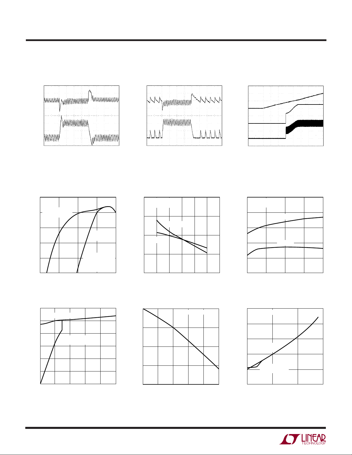
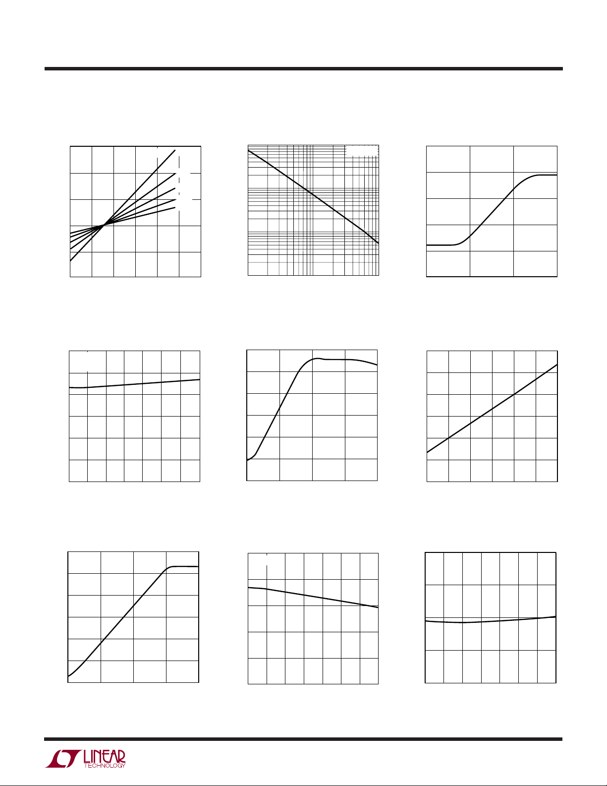
TYPICAL PERFOR A CE CHARACTERISTICS
Transient Response
Transient Response
(Discontinuous Mode)
Start-Up
V
OUT
50mV/DIV
I
L
5A/DIV
LOAD STEP 0A TO 10A
= 15V
V
IN
V
= 2.5V
OUT
FCB = 0V
FIGURE 9 CIRCUIT
Efficiency vs Load Current
100
DISCONTINUOUS
90
80
70
EFFICIENCY (%)
60
50
0.001
MODE
0.01
LOAD CURRENT (A)
20µs/DIV
= 10V
V
IN
V
OUT
EXTV
FIGURE 9 CIRCUIT
0.1
CONTINUOUS
MODE
= 2.5V
= 5V
CC
1
1778 G03
1778 G01
10
V
OUT
50mV/DIV
I
L
5A/DIV
LOAD STEP 1A TO 10A
= 15V
V
IN
V
= 2.5V
OUT
FCB = INTV
CC
FIGURE 9 CIRCUIT
Efficiency vs Input Voltage
100
FCB = 5V
FIGURE 9 CIRCUIT
95
I
LOAD
90
I
= 10A
LOAD
EFFICIENCY (%)
85
80
0
5101520
INPUT VOLTAGE (V)
20µs/DIV
= 1A
1778 G02
25 30
1778 G04
RUN/SS
2V/DIV
V
OUT
1V/DIV
I
L
5A/DIV
VIN = 15V
= 2.5V
V
OUT
R
= 0.25Ω
LOAD
Frequency vs Input Voltage
300
FCB = 0V
FIGURE 9 CIRCUIT
280
260
240
FREQUENCY (kHz)
220
200
5
I
10
INPUT VOLTAGE (V)
50ms/DIV
= 10A
OUT
I
= 0A
OUT
15
1778 G19
20
25
1778 G05
Frequency vs Load Current
300
CONTINUOUS MODE
250
200
150
100
FREQUENCY (kHz)
50
0
0
DISCONTINUOUS
MODE
2468
LOAD CURRENT (A)
4
1778 G26
Load Regulation
0
–0.1
(%)
–0.2
OUT
∆V
–0.3
10
–0.4
2
0
LOAD CURRENT (A)
4
FIGURE 9 CIRCUIT
6
8
1778 G06
10
ITH Voltage vs Load Current
2.5
FIGURE 9 CIRCUIT
2.0
1.5
CONTINUOUS
VOLTAGE (V)
1.0
TH
I
0.5
0
0
MODE
DISCONTINUOUS
MODE
5
LOAD CURRENT (A)
10
15
1778 G07
1778fb
UW
TEMPERATURE (°C)
–50
0.78
FEEDBACK REFERENCE VOLTAGE (V)
0.79
0.80
0.81
0.82
–25 0 25 50
1778 G12
75 100 125
TYPICAL PERFOR A CE CHARACTERISTICS
Current Sense Threshold
vs ITH Voltage
300
RNG
2V
=
V
On-Time vs ION Current
10k
V
VON
= 0V
LTC1778/LTC1778-1
On-Time vs VON Voltage
1000
I
ION
= 30µA
200
100
0
–100
CURRENT SENSE THRESHOLD (mV)
–200
0
1.0 1.5 2.0
0.5
ITH VOLTAGE (V)
On-Time vs Temperature
300
I
= 30µA
ION
= 0V
V
VON
250
200
150
ON-TIME (ns)
100
50
1.4V
1V
0.7V
0.5V
2.5 3.0
1778 G08
1k
ON-TIME (ns)
100
10
1
ION CURRENT (µA)
Current Limit Foldback
150
125
100
= 1V
V
RNG
75
50
25
10 100
1778 G20
800
600
400
ON-TIME (ns)
200
0
0
1
VON VOLTAGE (V)
Maximum Current Sense
Threshold vs V
300
250
200
150
100
50
RNG
2
Voltage
3
1778 G21
0
–50
–25 0
Maximum Current Sense
Threshold vs RUN/SS Voltage
150
125
100
MAXIMUM CURRENT SENSE THRESHOLD (mV)
= 1V
V
RNG
75
50
25
0
1.5
2 2.5 3 3.5
RUN/SS VOLTAGE (V)
50 100 125
25 75
TEMPERATURE (°C)
1778 G22
1778 G23
MAXIMUM CURRENT SENSE THRESHOLD (mV)
0
0
0.2 0.4 0.6 0.8
VFB (V)
Maximum Current Sense
Threshold vs Temperature
150
V
= 1V
RNG
140
130
120
110
MAXIMUM CURRENT SENSE THRESHOLD (mV)
100
–50 –25
0
TEMPERATURE (°C)
50
25
75
1778 G09
100
1778 G11
125
MAXIMUM CURRENT SENSE THRESHOLD (mV)
0
0.5
0.75
1.0 1.25 1.5
V
VOLTAGE (V)
RNG
1.75 2.0
Feedback Reference Voltage
vs Temperature
1778 G10
1778fb
5
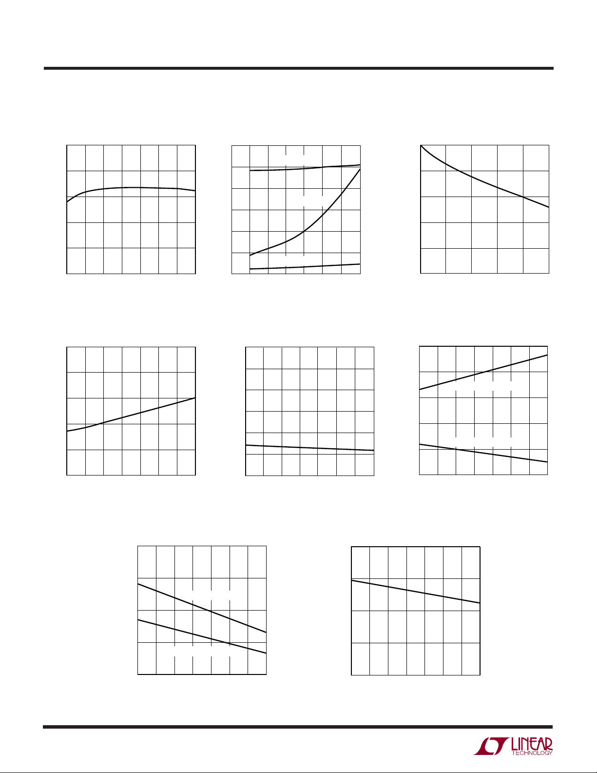
LTC1778/LTC1778-1
TEMPERATURE (C)
–50
2.0
UNDERVOLTAGE LOCKOUT THRESHOLD (V)
2.5
3.0
3.5
4.0
–25 0 25 50
1778 G18
75 100 125
UW
TYPICAL PERFOR A CE CHARACTERISTICS
Input and Shutdown Currents
Error Amplifier g
2.0
1.8
vs Temperature
m
vs Input Voltage
1200
1000
EXTVCC OPEN
INTV
Load Regulation
CC
60
50
SHUTDOWN CURRENT (µA)
0
–0.1
1.6
(mS)
m
g
1.4
1.2
1.0
–50 –25
25
0
TEMPERATURE (°C)
EXTVCC Switch Resistance
vs Temperature
10
8
6
4
SWITCH RESISTANCE (Ω)
CC
2
EXTV
800
600
400
INPUT CURRENT (µA)
200
50
75
100
125
1778 G13
0
0
510
SHUTDOWN
EXTVCC = 5V
20 30 35
15 25
INPUT VOLTAGE (V)
1778 G24
40
30
20
10
0
–0.2
(%)
CC
–0.3
∆INTV
–0.4
–0.5
10
0
INTVCC LOAD CURRENT (mA)
30
40
20
50
1778 G25
RUN/SS Pin Current
FCB Pin Current vs Temperature
0
–0.25
–0.50
–0.75
–1.00
FCB PIN CURRENT (µA)
–1.25
vs Temperature
3
2
1
0
FCB PIN CURRENT (µA)
–1
PULL-DOWN CURRENT
PULL-UP CURRENT
0
–50 –25
6
25
0
TEMPERATURE (°C)
RUN/SS THRESHOLD (V)
50
75
100
125
1778 G14
RUN/SS Latchoff Thresholds
vs Temperature
5.0
4.5
LATCHOFF ENABLE
4.0
3.5
3.0
–50
LATCHOFF THRESHOLD
–25 0 25 50
TEMPERATURE (°C)
–1.50
–50
–25 0
75 100 125
1778 G17
50 100 125
25 75
TEMPERATURE (°C)
1778 G15
–2
–50 –25
25
0
TEMPERATURE (°C)
Undervoltage Lockout Threshold
vs Temperature
50
75
100
125
1778 G16
1778fb

LTC1778/LTC1778-1
U
UU
PI FU CTIO S
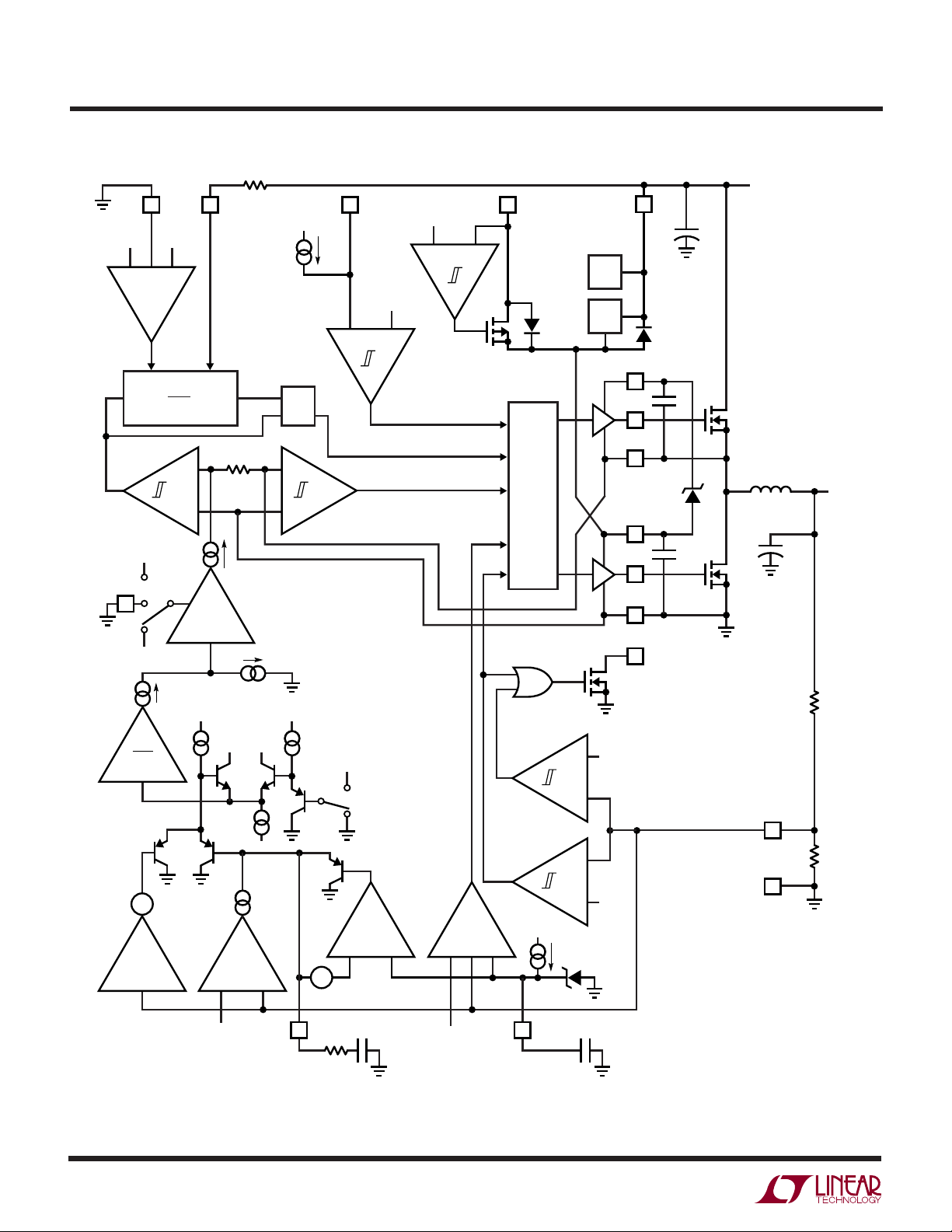
RUN/SS (Pin 1): Run Control and Soft-Start Input. A
capacitor to ground at this pin sets the ramp time to full
output current (approximately 3s/µF) and the time delay
for overcurrent latchoff (see Applications Information).
Forcing this pin below 0.8V shuts down the device.
PGOOD (Pin 2, LTC1778): Power Good Output. Open
drain logic output that is pulled to ground when the output
voltage is not within ±7.5% of the regulation point.
(Pin 2, LTC1778-1): On-Time Voltage Input. Voltage
V
ON
trip point for the on-time comparator. Tying this pin to the
output voltage or an external resistive divider from the
output makes the on-time proportional to V
comparator input defaults to 0.7V when the pin is grounded
or unavailable (LTC1778) and defaults to 2.4V when the
pin is tied to INTVCC. Tie this pin to INTVCC in high V
applications to use a lower RON value.
V
(Pin 3): Sense Voltage Range Input. The voltage at
RNG
this pin is ten times the nominal sense voltage at maximum output current and can be set from 0.5V to 2V by a
resistive divider from INTVCC. The nominal sense voltage
defaults to 70mV when this pin is tied to ground, 140mV
when tied to INTVCC.
FCB (Pin 4): Forced Continuous Input. Tie this pin to
ground to force continuous synchronous operation at low
load, to INTVCC to enable discontinuous mode operation
at low load or to a resistive divider from a secondary output
when using a secondary winding.
I
(Pin 5): Current Control Threshold and Error Amplifier
TH
Compensation Point. The current comparator threshold
increases with this control voltage. The voltage ranges
from 0V to 2.4V with 0.8V corresponding to zero sense
voltage (zero current).
SGND (Pin 6): Signal Ground. All small-signal components and compensation components should connect to
this ground, which in turn connects to PGND at one point.
OUT
. The
OUT
ION (Pin 7): On-Time Current Input. Tie a resistor from V
to this pin to set the one-shot timer current and thereby set
the switching frequency.
VFB (Pin 8): Error Amplifier Feedback Input. This pin
connects the error amplifier input to an external resistive
divider from V
EXTVCC (Pin 9): External VCC Input. When EXTVCC ex-
ceeds 4.7V, an internal switch connects this pin to INTV
and shuts down the internal regulator so that controller
and gate drive power is drawn from EXTVCC. Do not exceed
7V at this pin and ensure that EXTVCC < VIN.
VIN (Pin 10): Main Input Supply. Decouple this pin to
PGND with an RC filter (1Ω, 0.1µF).
INTVCC (Pin 11): Internal 5V Regulator Output. The driver
and control circuits are powered from this voltage. Decouple this pin to power ground with a minimum of 4.7µF
low ESR tantalum capacitor.
BG (Pin 12): Bottom Gate Drive. Drives the gate of the
bottom N-channel MOSFET between ground and INTVCC.
PGND (Pin 13): Power Ground. Connect this pin closely to
the source of the bottom N-channel MOSFET, the (–)
terminal of C
SW (Pin 14): Switch Node. The (–) terminal of the bootstrap capacitor CB connects here. This pin swings from a
diode voltage drop below ground up to VIN.
TG (Pin 15): Top Gate Drive. Drives the top N-channel
MOSFET with a voltage swing equal to INTVCC superimposed on the switch node voltage SW.
BOOST (Pin 16): Boosted Floating Driver Supply. The (+)
terminal of the bootstrap capacitor CB connects here. This
pin swings from a diode voltage drop below INTVCC up to
V
+ INTVCC.
IN
.
OUT
and the (–) terminal of CIN.
VCC
IN
CC
1778fb
7
LTC1778/LTC1778-1
U
U
W
FU CTIO AL DIAGRA
R
ON
**
I
7
ON
R
SQ
20k
+
–
+
I
REV
–
×
0.7V22.4V
1
tON = (10pF)
1.4V
V
RNG
3
0.7V
V
V
I
CMP
ON
I
VON
ION
1µA
V
IN
V
0.8V
REF
5V
REG
10
BOOST
16
TG
15
SW
14
INTV
CC
11
BG
12
PGND
13
PGOOD*
2
IN
+
C
IN
C
B
M1
L1
D
B
V
OUT
+
C
C
VCC
M2
OUT
FCB
4
–
F
0.8V
+
4.7V
+
–
SHDN
FCNT
ON
OV
9
SWITCH
EXTV
LOGIC
CC
1
240k
I
+
–
×4
LTC1778
*
LTC1778-1
**
THB
0.8V
3.3µA
0.74V
Q2
Q4
Q6
Q3
Q1
EA
–
+
0.8V
1V
Q5
0.6V
RUN
SHDN
1
RUN/SS
SS
–
+
+
–
0.6V
C
I
5
C1
TH
R
C
UV
OV
1.2µA
6V
+
–
+
0.86V
–
C
SS
V
FB
8
SGND
6
1778 FD
R2
R1
8
1778fb
 Loading...