

Linear Technology LTC1771 Datasheet
LTC1771
Final Electrical Specifications
Low Quiescent Current
High Efficiency Step-Down
DC/DC Controller
FEATURES
■
Very Low Standby Current: 10µA
■
Available in Space-Saving 8-Lead MSOP Package
■
High Output Currents
■
Wide VIN Range: 2.8V to 20V Operation
■
V
Range: 1.23V to 18V
OUT
■
High Efficiency: Over 93% Possible
■
±2% Output Accuracy
■
Very Low Dropout Operation: 100% Duty Cycle
■
Current Mode Operation for Excellent Line and
Load Transient Response
■
Defeatable Burst ModeTM Operation
■
Short-Circuit Protected
■
Optional Programmable Soft-Start
■
Micropower Shutdown: IQ = 2µA
U
APPLICATIO S
■
Cellular Telephones and Wireless Modems
■
1- to 4-Cell Lithium-Ion-Powered Applications
■
Portable Instruments
■
Battery-Powered Equipment
■
Battery Chargers
■
Scanners
U
February 2000
DESCRIPTIO
The LTC®1771 is a high efficiency current mode stepdown DC/DC controller that draws as little as 10µA DC
supply current to regulate the output at no load while
maintaining high efficiency for loads up to several amps.
The LTC1771 drives an external P-channel power MOSFET
using a current mode, constant off-time architecture. An
external sense resistor is used to program the operating
current level. Current mode control provides short-circuit
protection, excellent transient response and controlled
start-up behavior. Burst Mode operation enables the
LTC1771 to maintain high efficiency down to extremely
low currents. Shutdown mode further reduces the supply
current to a mere 2µA. For low noise applications, Burst
Mode operation can be easily disabled with the MODE pin.
Wide input supply range of 2.8V to 18V (20V maximum)
and 100% duty cycle operation for low dropout make the
LTC1771 ideal for a wide variety of battery-powered applications where maximizing battery life is important.
The LTC1771’s availability in both 8-lead MSOP and SO
packages provides for a minimum area solution.
, LTC and LT are registered trademarks of Linear Technology Corporation.
Burst Mode is a trademark of Linear Technology Corporation.
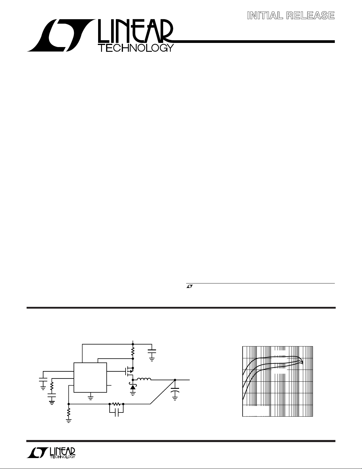
TYPICAL APPLICATIO
V
IN
C
SS
0.01µF
R
C
10k
C
22OpF
RUN/SS
I
TH
V
FB
C
R1
1M
1%
Figure 1. High Efficiency Step-Down Converter
LTC1771
GND
U
V
IN
4.5V TO 18V
100
90
80
70
EFFICIENCY (%)
60
50
40
L1
15µH
10µF
25V
CER
V
OUT
3.3V
C
OUT
150µF
6.3V
2A
1771 F01
+
R
SENSE
0.05Ω
SENSE
PGATE
MODE
M1
Si6447DQ
V
IN
R2
1.64M
1%
5pF
Information furnished by Linear Technology Corporation is believed to be accurate and reliable.
However, no responsibility is assumed for its use. Linear Technology Corporation makes no representation that the interconnection of its circuits as described herein will not infringe on existing patent rights.
UPS5817
LTC1771 Efficiency
VIN = 5V
VIN = 10V
VIN = 15V
V
= 3.3V
OUT
= 0.05Ω
R
SENSE
0.1 1 100 1000 10000
10
LOAD CURRENT (mA)
1771 F01b
1
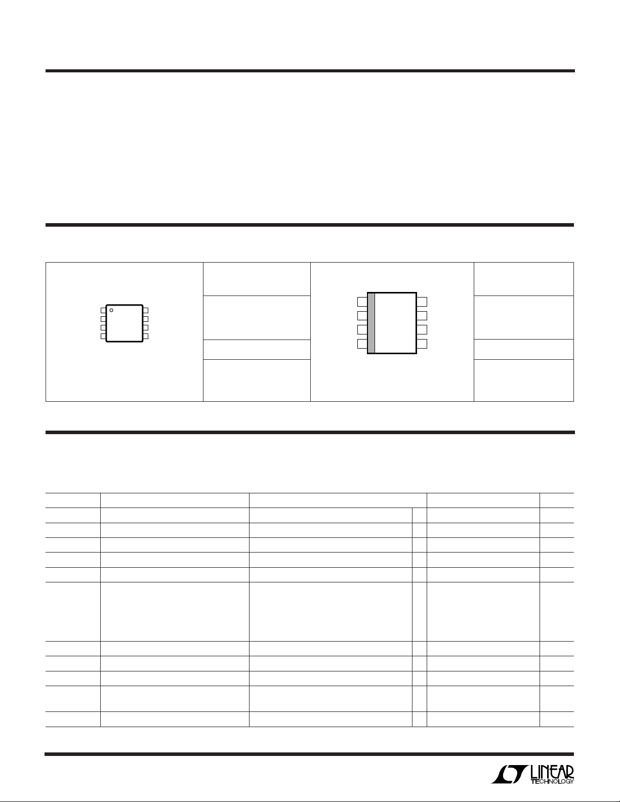
LTC1771
RUN/SS
I
TH
V
FB
GND
1
2
3
4
8
7
6
5
MODE
SENSE
V
IN
PGATE
TOP VIEW
MS8 PACKAGE
8-LEAD PLASTIC MSOP
TOP VIEW
MODE
SENSE
V
IN
PGATE
RUN/SS
I
TH
V
FB
GND
S8 PACKAGE
8-LEAD PLASTIC SO
1
2
3
4
8
7
6
5
WWWU
ABSOLUTE AXI U RATI GS
(Note 1)
Input Supply Voltage (VIN)........................ –0.3V to 20V
Peak Driver Output Current < 10µs (PGATE) ............. 1A
RUN/SS Voltage ........................... – 0.3V to (VIN + 0.3V)
MODE Voltage .......................................... –0.3V to 20V
ITH, VFB Voltage .......................................... –0.3V to 5V
SENSE Voltage (VIN > 12V)...(VIN – 12V) to (VIN + 0.3V)
SENSE Voltage (VIN ≤ 12V) .......... –0.3V to (VIN + 0.3V)
UU
W
PACKAGE/ORDER I FOR ATIO
ORDER PART
NUMBER
LTC1771EMS8
MS8 PART MARKING
T
= 125°C, θJA = 150°C/W
JMAX
LTKD
Junction Temperature (Note 2)............................ 125°C
Operating Temperature Range (Note 3)
LTC1771E......................................... –40°C to 85°C
LTC1771I ......................................... – 40°C to 85°C
Storage Temperature Range ................. –65°C to 150°C
Lead Temperature (Soldering, 10 sec).................. 300°C
ORDER PART
NUMBER
LTC1771ES8
LTC1771IS8
S8 PART MARKING
T
= 125°C, θJA = 110°C/W
JMAX
1771
1771I
Consult factory for Military grade parts.
ELECTRICAL CHARACTERISTICS
The ● denotes specifications which apply over the full operating temperature range, otherwise specifications are TA = 25°C.
VIN = 10V, V
SYMBOL PARAMETER CONDITIONS MIN TYP MAX UNITS
V
FB
I
FB
I
SUPPLY
∆V
LINEREG
∆V
LOADREG
I
Q
∆V
SENSE(MAX)
∆V
SENSE(MIN)
∆V
SENSE(SLEEP)
t
OFF
V
MODE
2
= open unless otherwise specified.
RUN
Feedback Voltage (Note 5) ● 1.205 1.230 1.255 V
Feedback Current (Note 5) ● 110 nA
No-Load Supply Current VIN = 10V, I
Reference Voltage Line Regulation VIN = 5V to 15V (Note 5) ● 0.003 0.03 %/V
Output Voltage Load Regulation ITH = 0.5V to 2V, Burst Disabled (Note 5) ● 0.25 1 %
Input DC Supply Current (Note 4)
Active Mode (PGATE = 0V) V
Sleep Mode (Note 6) V
Shutdown V
Short Circuit V
Maximum Current Sense Threshold VFB = V
Minimum Current Sense Threshold VFB = V
Sleep Current Sense Threshold ITH = 1V 50 mV
Switch Off Time VFB at Regulated Value 3.5 µs
Mode Pin Threshold V
= 2.8V to 18V 150 235 µA
IN
= 2.8V to 18V, VFB = 1.5V 9 15 µA
IN
= 2.8V to 18V, V
IN
= 2.8V to 18V, VFB = 0V 175 275 µA
IN
REF
REF
= 0V 70 µs
V
FB
Rising ● 0.5 1.3 2 V
MODE
= 0 (Note 6) 10 µA
LOAD
= 0V 2 6 µA
RUN
– 20mV ● 110 140 180 mV
+ 10mV, Burst Disabled –25 mV
LTC1771
ELECTRICAL CHARACTERISTICS
The ● denotes specifications which apply over the full operating temperature range, otherwise specifications are TA = 25°C.
VIN = 10V, V
SYMBOL PARAMETER CONDITIONS MIN TYP MAX UNITS
V
RUN/SS
I
RUN
PGATE tr, t
= open unless otherwise specified.
RUN
RUN/SS Pin Threshold V
Source Current V
PGATE Transition Time (Note 7)
f
Rise Time C
Fall Time C
Rising ● 0.5 1.0 2 V
RUN/SS
= 0V, VIN = 2.8V to 18V 0.3 1 3 µA
RUN
= 2000pF 80 ns
LOAD
= 2000pF 90 ns
LOAD
Note 1: Absolute Maximum Ratings are those values beyond which the life
of a device may be impaired.
Note 2: T
dissipation P
Note 3: The LTC1771E is guaranteed to meet performance specifications
from 0°C to 70°C. Specifications over the –40°C to 85°C operating
temperature range are assured by design, characterization and correlation
with statistical process controls. The LTC1771I is guaranteed and tested
over the –40°C to 85°C operating temperature range.
is calculated from the ambient temperature TA and power
J
according to the following formulas:
D
LTC1771S8: TJ = TA + (PD)(110°C/W)
LTC1771MS8: T
U
= TA + (PD)(150°C/W)
J
UU
PI FU CTIO S
RUN/SS (Pin 1): The voltage level on this pin controls
shutdown/run mode (ground = shutdown, open/high =
run). Connecting an external capacitor to this pin provides
soft-start.
ITH (Pin 2): Error Amplifier Compensation Point. The
current comparator threshold increases with this control
voltage. Nominal voltage range for this pin is 0V to 3V.
VFB (Pin 3): Feedback of Output Voltage for Comparison
to Internal 1.23V Reference. An external resistive divider
across the output is returned to this pin.
GND (Pin 4): Ground Pin.
Note 4: Dynamic supply current is higher due to the gate charge being
delivered at the switching frequency. See Applications Information.
Note 5: The LTC1771 is tested in a feedback loop that servos V
balance point for the error amplifier (V
Note 6: No-load supply current consists of sleep mode current (9µA
typical) plus a small switching component necessary to overcome
Schottky diode leakage and feedback resistor current.
Note 7: t
and tf measured at 10% to 90% levels.
r
= 1.23V).
ITH
to the
FB
PGATE (Pin 5): High Current Gate Driver for External
P-Channel MOSFET Switch. Voltage swing is from ground
to VIN.
VIN (Pin 6): Main Input Voltage Supply Pin.
SENSE (Pin 7): Current Sense Input for Monitoring Switch
Current. Maximum switch current and Burst Mode
threshold is programmed with an external resistor between SENSE and VIN.
MODE (Pin 8): Burst Mode Enable/Disable Pin. Connecting this pin to VIN (or above 2V) enables Burst Mode
operation, while connecting this pin to ground disables
Burst Mode operation. Do not leave floating.
3
LTC1771
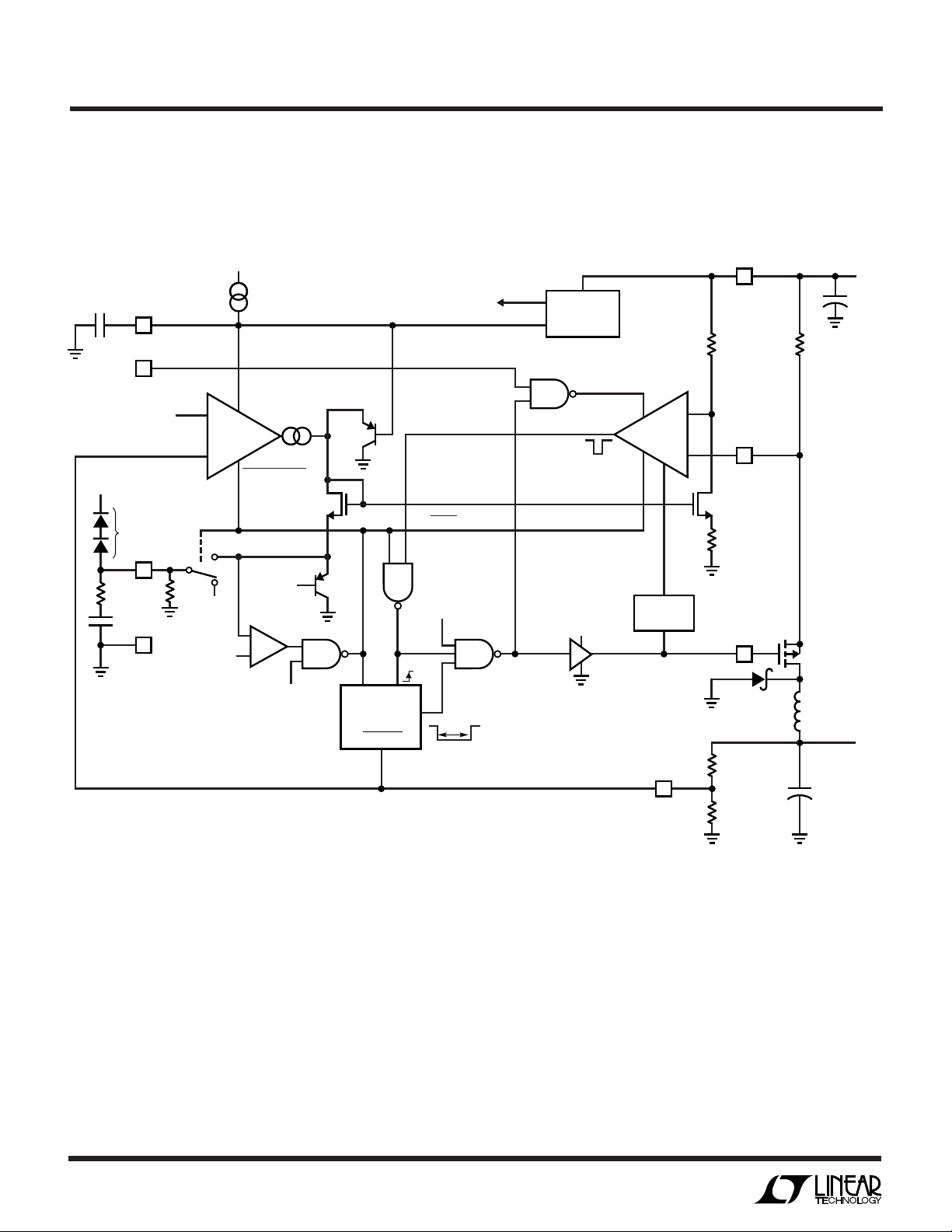
UU
W
FUNCTIONAL BLOCK DIAGRA
V
IN
+
EA
–
1V
1V
1µA
ON
10% CURRENT
–
B
+
SOFT-START
2V
C
SS
RUN/SS
1
MODE
(BURST ENABLE)
8
1.23V
V
OUT
*
I
TH
2
R
C
C
C
GND
4
SLEEP
READY
READY
1.23V
REFERENCE
10% CURRENT
V
IN
C
ON
BLANKING
22k R
–
+
250k
V
IN
6
SENSE
7
SW
5
+
SENSE
V
IN
C
IN
*
OPTIONAL FOR FOLDBACK
CURRENT LIMITING
MODE
ON TRIGGER
1-SHOT
STRETCH
3.5µs
L
V
OUT
V
FB
3
+
C
OUT
1771 BD
4

OPERATIO
LTC1771
U
(Refer to Functional Block Diagram)
Main Control Loop
The LTC1771 uses a constant off-time, current mode
step-down architecture. During normal operation, the
P-channel MOSFET is turned on at the beginning of each
cycle and turned off when the current comparator C
triggers the 1-shot timer. The external MOSFET switch
stays off for the 3.5µs 1-shot duration and then turns back
on again to begin a new cycle. The peak inductor current
at which C triggers the 1-shot is controlled by the voltage
on Pin 3 (ITH), the output of the error amplifier EA. An
external resistive divider connected between V
ground allows EA to receive an output feedback voltage
VFB. When the load current increases, it causes a slight
decrease in VFB relative to the 1.23V reference, which in
turn causes the ITH voltage to increase until the average
inductor current matches the new load current.
The main control loop is shut down by pulling Pin 1
(RUN/SS) low. Releasing RUN/SS allows an internal 1µA
current source to charge soft-start capacitor CSS. When
CSS reaches 1V, the main control loop is enabled with the
ITH voltage clamped at approximately 40% of its maximum value. As CSS continues to charge, ITH is gradually
released allowing normal operation to resume.
Burst Mode Operation
The LTC1771 provides outstanding low current efficiency
and ultralow no-load supply current by using Burst Mode
operation when the MODE pin is pulled above 2V. During
Burst Mode operation, short burst cycles of normal switching are followed by a longer idle period with the switch off
and the load current is supplied by the output capacitor.
During this idle period, only the minimum required circuitry—1.23V reference and error amp—are left on, and
the supply current is reduced to 9µA. At no load, the output
capacitor is still discharged very slowly by leakage current
in the Schottky diode and feedback resistor current resulting in very low frequency burst cycles that add a few more
microamps to the supply current.
OUT
and
Burst Mode operation is provided by clamping the minimum ITH voltage at 1V which represents about 25% of
maximum load current. If the load falls below this level, i.e.
the ITH voltage tries to fall below 1V, the burst comparator
B switches state signaling the LTC1771 to enter sleep
mode. During this time, EA is reduced to 10% of its normal
operating current and the external compensation capacitor is disconnected and clamped to 1V so that the EA can
drive its output with the lower available current. As the load
discharges the output capacitor, the internal ITH voltage
increases. When it exceeds 1V the burst comparator exits
sleep mode, reconnects the external compensation components to the error amplifier output, and returns EA to full
power along with the other necessary circuitry. This
scheme (patent pending) allows the EA to be reduced to
such a low operating current during sleep mode without
adding unacceptable delay to wake up the LTC1771 due to
the compensation capacitor on ITH required for stability in
normal operation.
Burst Mode operation can be disabled by pulling the
MODE pin to ground. In this mode of operation, the burst
comparator B is disabled and the ITH voltage allowed to go
all the way to 0V. The load can now be reduced to about 1%
of maximum load before the loop skips cycles to maintain
regulation. This mode provides a low noise output spectrum, useful for reducing both audio and RF interference,
at the expense of reduced efficiency at light loads.
Off-Time
The off-time duration is 3.5µs when the feedback voltage
is close to the reference voltage; however, as the feedback
voltage drops, the off-time lengthens and reaches a maximum value of about 70µs when VFB is zero. This ensures
that the inductor current has enough time to decay when
the reverse voltage across the inductor is low such as
during short circuit, thus protecting the MOSFET and
inductor.
5
 Loading...