

Linear Technology LTC1759 Datasheet
FEATURES
■
Single Chip Smart Battery Charger Controller
■
100% Compliant (Rev 1.0) SMBus Support
Allows for Operation with or without Host
■
SMBus Accelerator Improves SMBus Timing
■
Hardware Interrupt and SMBAlert Response
Eliminate Interrupt Polling
■
High Efficiency Synchronous Buck Charger
■
0.5V Dropout Voltage; Maximum Duty Cycle > 99.5%
■
AC Adapter Current Limit Maximizes Charge Rate*
■
1% Voltage Accuracy; 5% Current Accuracy
■
Up to 8A Charging Current Capability
■
Dual 10-Bit DACs for Charger Voltage and Current
Programming
■
User-Selectable Overvoltage and Overcurrent Limits
■
High Noise Immunity Thermistor Sensor
■
Small 36-Lead Narrow (0.209") SSOP Package
U
APPLICATIO S
■
Portable Computers
■
Portable Instruments
■
Docking Stations
*US Patent Number 5,723,970
LTC1759
Smart Battery Charger
U
DESCRIPTIO
The LTC®1759 Smart Battery Charger is a single chip
charging solution that dramatically simplifies construction of an SBS compliant system. The LTC1759 implements a Level 2 charger function whereby the charger can
be programmed by the battery or by the host. A thermistor
on the battery being charged is monitored for temperature, connectivity and battery type information. The SMBus
interface remains alive when the AC power adapter is
removed and responds to all SMBus activity directed to it,
including thermistor status (via the ChargerStatus command). The charger also provides an interrupt to the host
whenever a status change is detected (e.g., battery
removal,
Charging current and voltage are restricted to chemistry
specific limits for improved system safety and reliability.
Limits are programmable by two external resistors. Additionally, the maximum average current from the AC adapter
is programmable to avoid overloading the adapter when
simultaneously supplying load current and charging current. When supplying system load current, charging current is automatically reduced to prevent adapter overload.
AC adapter connection).
, LTC and LT are registered trademarks of Linear Technology Corporation.
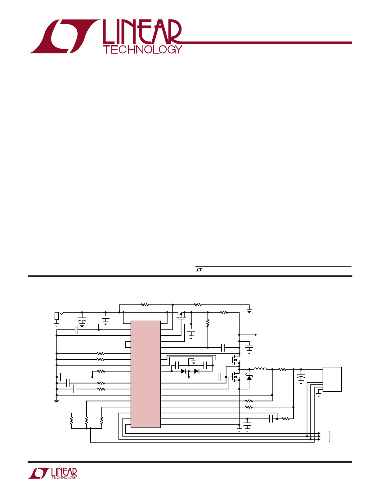
TYPICAL APPLICATIO
ADAPTER
INPUT
AC
0.1µF
1µF
0.33µF
V
DD
475k
+
0.68µF
10µF
35V
Al
10k
0.1µF
V
DD
33k
33k
3.83k
1.5k
1k
1k
U
15.8k
LTC1759
7
UV
16
V
DD
4
SYNC
5
SDB
12
CHGEN
25
V
LIMIT
24
I
LIMIT
18
DGND
17
I
SET
28
PROG
27
V
C
11
COMP1
6
AGND
20
RNR
19
THERM
14
SDA
15
SCL
13
INTB
DCIN
DCDIV
INFET
V
CLP
CLN
TGATE
BOOSTC
GBIAS
BOOST
BGATE
SPIN
SENSE
BAT1
BAT2
V
PGND
22
21
8
32
CC
9
10
2
2.2µF
33
34
1
3
SW
35
30
29
31
23
26
SET
36
Figure 1. 4A SMBus Smart Battery Charger
1k
499Ω
0.47µF
0.1µF
0.68µF
0.033Ω
1µF
SYSTEM
POWER
22µF
15µH
200Ω
200Ω
0.047µF
0.015µF
0.025Ω
68Ω
+
22µF
INTB
SCL
SDA
SMART
BATTERY
SMBus
TO
HOST
1759 F01
1
LTC1759
WW
W
U
ABSOLUTE MAXIMUM RATINGS
(Note 1)
Voltage at VCC, UV, BAT1, CLP,CLN, SPIN,
SENSE with respect to AGND ....................–0.3V to 27V
Voltage at DCIN, BAT2 with Respect
to DGND ....................................................–0.3V to 27V
Voltage at INTB, SDA, SCL, DCDIV with Respect
to DGND ..................................................... – 0.3V to 7V
BOOST, BOOSTC Voltage with Respect to VCC........ 10V
Voltage at VDD with Respect to DGND ........ –0.3V to 7V
SW Voltage with Respect to AGND .............. –2V to V
GBIAS, SYNC ............................................ – 0.3V to 10V
VC, PROG, V
Voltage with Respect
SET
to AGND ......................................................– 0.3V to 7V
TGATE, BGATE Current Continuous .................. ±200mA
TGATE, BGATE Output Energy (per Cycle) ................ 2µJ
PGND, DGND with Respect to AGND .................... ±0.3V
Current into Any Pin ......................................... ±100mA
Operating Ambient Temperature Range...... 0°C to 70°C
Operating Junction
Temperature Range .............................. – 40°C to 125°C
Storage Temperature ........................... –65°C to 150°C
Lead Temperature (Soldering, 10 sec)................. 300°C
CC
U
W
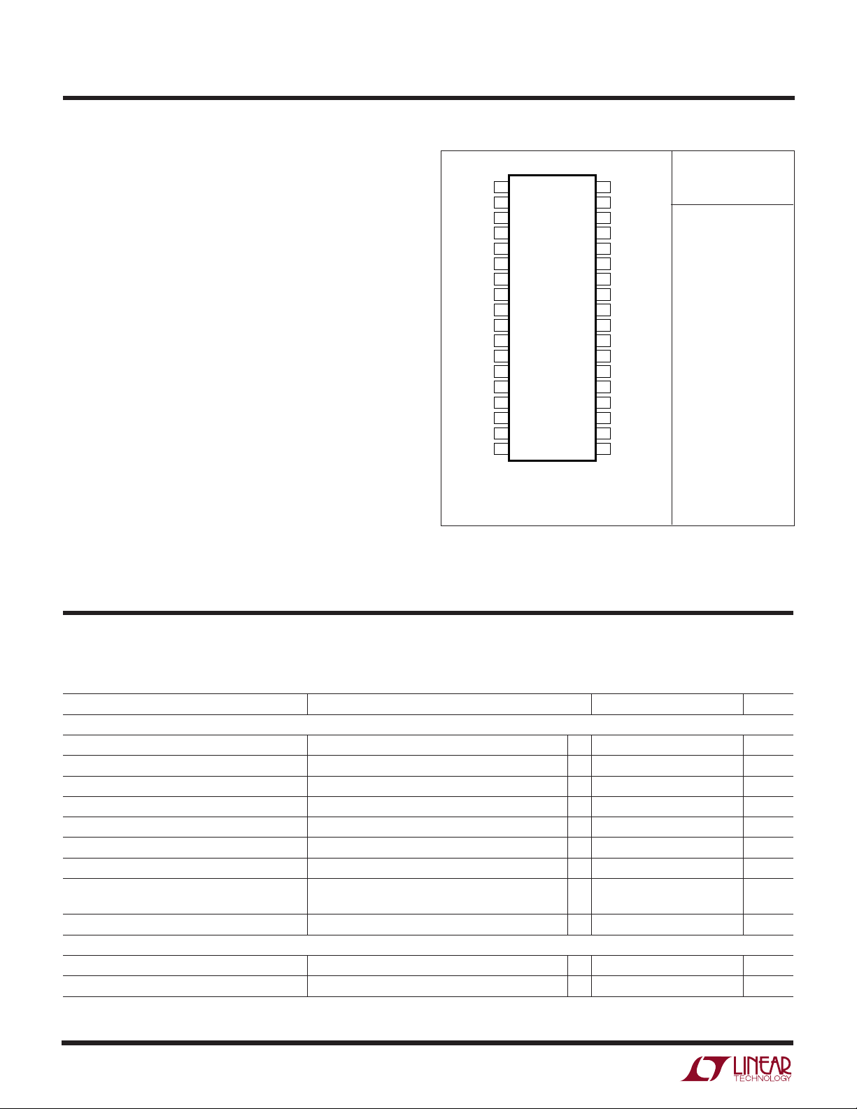
PACKAGE/ORDER INFORMATION
TOP VIEW
1
BOOST
2
TGATE
3
SW
4
SYNC
5
SDB
6
AGND
7
UV
8
INFET
9
CLP
10
CLN
11
COMP1
12
CHGEN
13
INTB
14
SDA
15
SCL
16
V
DD
17
I
SET
18
DGND
G PACKAGE
36-LEAD PLASTIC SSOP
T
= 125°C, θJA = 85°C/W
JMAX
Consult factory for Industrial and Military grade parts.
36
35
34
33
32
31
30
29
28
27
26
25
24
23
22
21
20
19
PGND
BGATE
GBIAS
BOOSTC
V
CC
BAT1
SPIN
SENSE
PROG
V
C
V
SET
V
LIMIT
I
LIMIT
BAT2
DCIN
DCDIV
RNR
THERM
ORDER PART
NUMBER
LTC1759CG
U
ELECTRICAL CHARACTERISTICS
The ● denotes specifications which apply over the full operating temperature range (TJ = 0°C to 100°C), otherwise specifications are
T
= 25°C. V
A
PARAMETER CONDITIONS MIN TYP MAX UNITS
Supply and Reference
DCIN, VCC Operating Voltage ● 11 24 V
VCC Operating Current VCC ≤ 24V ● 12 20 mA
DCIN Operating Current V
UV Lockout Threshold Voltage on UV Pin Rising ● 6.3 6.7 7.15 V
UV Pin Input Current 0V ≤ VUV ≤ 8V ● –1 5 µA
Battery Discharge Current VUV ≤ 0.4V, All Connected Pins 40 80 µA
VDD Operating Voltage ● 3.0 5.5 V
VDD Operating Current Charging, VDD = 5.5V, Shorted Thermistor 1.35 2 mA
VDD Undervoltage Lockout ● 1.6 2.2 2.9 V
Switching Regulator
Charging Voltage Accuracy (Notes 3, 5) 2.465V ≤ V
Charging Current Accuracy (Note 3) R
= DCIN = 18V, V
CC
= 12.6V, VDD = 3.3V unless otherwise specified.
BAT1, 2
= 24V ● 85 150 µA
DCIN
Not Charging, V
Tolerance = 1% –5 5 %
SET
= 5.5V 80 150 µA
DD
≤ V
BAT2
MAX
● –1 1 %
2
LTC1759
ELECTRICAL CHARACTERISTICS
The ● denotes specifications which apply over the full operating temperature range (TJ = 0°C to 100°C), otherwise specifications are
T
= 25°C. V
A
PARAMETER CONDITIONS MIN TYP MAX UNITS
BOOST Pin Current V
V
Threshold to Turn T
BOOST
(Note 6) Low to High
BOOSTC Pin Current V
Sense Amplifier CA1 Gain and Input Offset Voltage 11V ≤ VCC ≤ 24V, 0V ≤ V
(With R
(Measured Across R
CA1 Bias Current (SENSE, BAT1) V
CA1 Input Common Mode Range ● –0.25 VCC – 0.3 V
SPIN Input Current V
CL1 Turn-On Threshold 0.5mA Output Current 87 92 97 mV
CL1 Transconductance Output Current from 50µA to 500µA 0.5 1 3 mho
CLP Input Current 0.5mA Output Current 1 3 µA
CLN Input Current 0.5mA Output Current 0.8 2 mA
CA2 Transconductance VC = 1V, IVC = ±1µA 150 200 300 µmho
VA Transconductance (Note 5) Ouput Current from 50µA to 500µA 0.21 0.6 1 mho
Gate Drivers
V
GBIAS
V
High (V
TGATE
V
High I
BGATE
V
Low (V
TGATE
V
Low I
BGATE
INFET “ON” Clamping Voltage (VCC – V
INFET “ON” Drive Current V
INFET “OFF” Clamping Voltage VCC Not Connected, I
INFET “OFF” Drive Current VCC = 12.4V, (VCC – V
V
, V
TGATE
Trip Points
DCDIV Threshold V
DCDIV Hysteresis 25 mV
DCDIV Input Bias Current V
Power-Fail Indicator (V
Power-Fail Indicator Hysteresis (V
SYNC Pin Threshold 0.9 1.4 2.0 V
SYNC Pin Input Current V
= DCIN = 18V, V
CC
= 12.6V, VDD = 3.3V unless otherwise specified.
BAT1, 2
= VSW + 8V, 0V ≤ VSW ≤ 20V
BOOST
TGATE High 2 3 mA
TGATE Low 2 3 mA
Off Measured at (V
GATE
BOOST
– VSW)
Hysteresis 0.25 V
= VCC + 8V 1 mA
BOOSTC
= RS3 = 200Ω)R
S2
TGAGE
TGATE
at Shutdown V
BGATE
) (Note 4) R
S1
– VSW)I
– VSW)I
) ● 6.5 7.8 9 V
INFET
≥ V
BAT2
) (Note 7) AC_PRESENT = 1, V
DCIN
≥ V
BAT2
) AC_PRESENT = 1, V
DCIN
= 4.93k ● 92 100 108 mV
SET
= 49.3k 7 10 13 mV
SET
= High ● –50 –120 µA
SDB
= Low (Shutdown) –10 µA
V
SDB
= High, V
SDB
= Low 10 µA
V
SDB
VCC ≥ 11V, I
TGATE
BGATE
TGATE
BGATE
INFET
= Low, I
SDB
DCDIV
DCDIV
SYNC
V
SYNC
SPIN
GBIAS
≤ 20mA ● 5.6 6.6 V
≤ 20mA ● 6.2 7.2 V
≤ 50mA ● 0.8 V
≤ 50mA ● 0.8 V
= VCC – 6V ● 820 mA
TGATE
Rising from 0.8V to 1.2V ● 0.9 1.0 1.1 V
= 1V ● 100 nA
= 0V –500 µA
= 2V –30 µA
BAT
= 12.6V ● 2mA
≤ 15mA, V
< –2µA 1.4 V
INFET
INFET
= I
BGATE
= 6V ● 0.84 0.89 0.94 V/V
DCIN
= 6V 0.02 V/V
DCIN
● 6.8 7.1 7.3 V
≤ 20V
= High ● 8.4 8.9 9.3 V
SDB
) ≥ 2V –2.5 mA
= 10µA ● 1V
3
LTC1759
ELECTRICAL CHARACTERISTICS
The ● denotes specifications which apply over the full operating temperature range (TJ = 0°C to 100°C), otherwise specifications are
T
= 25°C. V
A
PARAMETER CONDITIONS MIN TYP MAX UNITS
Thermistor Decoder (Note 11)
Combined Input Leakage on RNR and THERM 200 nA
Thermistor Trip (COLD/OR) R
Thermistor Trip (IDEAL/COLD) RNR = 10k ±1% ● 26.4 30 33.6 kΩ
Thermistor Trip (HOT/IDEAL) RNR = 10k ±1% ● 2.64 3 3.36 kΩ
Thermistor Trip (UR/HOT) RUR = 1k ±1% ● 440 500 560 Ω
DACs
Charging Current Resolution Guaranteed Monotonic Above I
Charging Current Granularity R
Wake-Up Charging Current (I
Charging Current Limit (I
I
SET RDS(ON)
I
SET IOFF
Charging Voltage Resolution Guaranteed Monotonic (2.5V ≤ V
Charging Voltage Granularity R
Charging Voltage Limit R
Logic Levels (Note 12)
SCL/SDA Input Low Voltage (VIL) ● 0.6 V
SCL/SDA Input High Voltage (VIH) ● 1.4 V
SDA Output Low Voltage (VOL)I
SCL/SDA Input Current (IIL)V
SCL/SDA Input Current (IIH)V
INTB Output Low Voltage (VOL)I
INTB Output Pull-Up Current V
CHGEN Output Low Voltage (VOL)I
CHGEN Output High Voltage (VOH)I
SDB Shutdown Threshold ● 12V
SDB Pin Current 0V ≤ V
Power-On Reset Duration VDD Ramp from 0V to > 3V in < 5µs 100 µs
= DCIN = 18V, V
CC
WAKE-UP
)R
MAX
= 12.6V, VDD = 3.3V unless otherwise specified.
BAT1, 2
= 475k ±1% ● 80 100 120 kΩ
WEAK
/16 10 bits
MAX
= 0 1 mA
ILIMIT
= 10k ±1% 2 mA
R
ILIMIT
R
= 33k ±1% 4 mA
ILIMIT
= Open (or Short to VDD)8mA
R
ILIMIT
) (Note 8) 80 mA
= 0 1023 mA
ILIMIT
= 10k ±1 % 2046 mA
R
ILIMIT
= 33k ±1 % 4092 mA
R
ILIMIT
R
= Open (or Short to VDD) 8184 mA
ILIMIT
25 Ω
V
= 2.7V ● 1 µA
ISET
≤ 21V) 10 bits
BAT
= 0 16 mV
VLIMIT
R
= 10k ±1% 16 mV
VLIMIT
= 33k ±1% 32 mV
R
VLIMIT
= 100k ±1% 32 mV
R
VLIMIT
R
= Open (or Short to VDD)32mV
VLIMIT
= 0 ● 8.33 8.432 8.485 V
VLIMIT
= 10k ±1% ● 12.50 12.64 12.72 V
R
VLIMIT
= 33k ±1% ● 16.67 16.864 16.97 V
R
VLIMIT
R
= 100k ±1% ● 20.82 21.056 21.18 V
VLIMIT
= Open (or Short to VDD) (Note 2) 32.736 V
R
VLIMIT
= 350µA ● 0.4 V
PULLUP
, V
SDA
SDA
PULLUP
INTB
OL
OH
= V
SCL
IL
, V
= V
SCL
IH
= 500µA ● 0.4 V
= V
OL
= 200µA ● 0.4 V
= –200µA ● VDD – 0.4 V
≤ 3V 8 µA
SDB
● 1 µA
● 1 µA
● 3.5 10 17.5 µA
4
LTC1759
ELECTRICAL CHARACTERISTICS
The ● denotes specifications which apply over the full operating temperature range (TJ = 0°C to 100°C), otherwise specifications are
T
= 25°C. V
A
PARAMETER CONDITIONS MIN TYP MAX UNITS
Charger Timing
V
, V
TGATE
TGATE, BGATE Peak Drive Current 10nF Load 1 A
Regulator Switching Frequency ● 170 200 230 kHz
Synchronization Frequency ● 240 280 kHz
Maximum Duty Cycle in Start-Up Mode (Note 9) ● 85 90 %
t
TIMEOUT
Cold or Underrange Battery
SMBus Timing (refer to System Management Bus Specification, Revision 1.0, section 2.1 for timing diagrams) (Note 12)
SCL Serial Clock High Period (t
SCL Serial Clock Low Period (t
SDA/SCL Rise Time (tr)C
SDA/SCL Fall Time (tf) ● 30 300 ns
SMBus Accelerator Boosted Pull-Up Current VDD = 3V ● 1 2.5 mA
Start Condition Setup Time (t
Start Condition Hold Time (t
SDA to SCL Rising-Edge Setup Time (t
SDA to SCL Falling-Edge Hold Time, ● 300 ns
Slave Clocking in Data (t
t
TIMEOUT
ChargingCurrent() and ChargingVoltage()
Commands (Note 10)
Note 1: Absolute Maximum Ratings are those values beyond which the life
of a device may be impaired.
Note 2: This limit is greater than the absolute maximum for the charger.
Therefore, there is no effective limitation on voltage when this option is
selected. If the charger is requested to charge with a higher voltage than
the nominal limit, the VOLTAGE_OR bit will be set.
Note 3: Total system accuracy from SMBus request to output voltage or
output current.
Note 4: Test Circuit #1.
Note 5: Voltage accuracy is calculated using measured reference voltage,
obtained from V
ratio.
Note 6: When supply and battery voltage differential is low, high oscillator
duty cycle is required. The LTC1759 has a unique design to achieve duty
cycle greater than 99% by skipping cycles. Only when V
the comparator threshold, will TGATE be turned off. See Applications
Information section.
= DCIN = 18V, V
CC
Rise/Fall Time 1nF Load 25 ns
BGATE
for Wake-Up Charging a ● 140 175 210 sec
HIGH
LOW
SU:STA
HD:STA
)
HD:DAT
Between Receiving Valid ● 140 175 210 sec
pin using Test Circuit #2, and VDAC resistor divider
SET
= 12.6V, VDD = 3.3V unless otherwise specified.
BAT1, 2
)I
)I
) ● 4.7 µs
) ● 4.0 µs
) ● 250 ns
SU:DAT
= 350µA, C
PULLUP
= 350µA, C
PULLUP
= 150pF ● 1000 ns
LOAD
drops below
BOOST
= 150pF ● 4 µs
LOAD
= 150pF ● 4.7 µs
LOAD
Note 7: Power failure bit is set when the battery voltage is above 89% of
the power adapter voltage (V
Note 8: The charger provides wake-up current when a battery is inserted
into the connector, prior to the battery requesting charging current and
voltage. See Smart Battery Charger Specification (Revision 1.0), section
6.1.3 and 6.1.8.
Note 9: In system start-up, C6 (boost capacitor) has no charge stored in it.
The LTC1759 will keep TGATE off, and turn BGATE on for 0.2µs, thus
charging C6. A comparator senses V
PWM mode when V
Note 10: Refer to Smart Battery Charge Specification (Revision 1.0),
section 6.1.2.
Note 11: Maximum total external capacitance on RNR and THERM pins
is 75pF.
Note 12: SMBus operation guaranteed by design from –40°C to 85°C.
BOOST
).
DCIN
and switches to the normal
is above its threshold.
BOOST
5
LTC1759
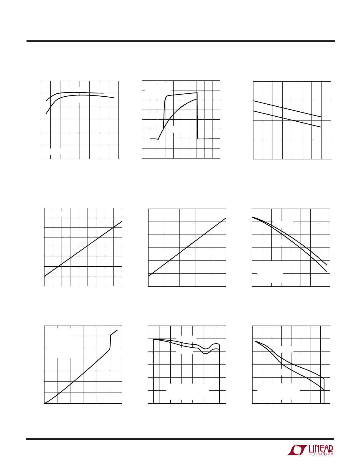
TEMPERATURE (°C)
0
DCDIV (V)
1.10
1.05
1.00
0.95
0.90
1759 G03
10 20 30 40 50 60 70 80
VDD = 5.5V
VDD = 3V
CHARGING CURRENT (mA)
256
1256 2256 3256 4256
OUTPUT CURRENT ERROR (mA)
1759 G06
0
–10
–20
–30
–40
–50
–60
R
ILIMIT
= 33k
V
IN
= 15V
V
OUT
= 12V
T
A
= 25°C
VDD = 5.5V
VDD = 3V
UW
TYPICAL PERFOR A CE CHARACTERISTICS
Charger Efficiency
100
95
90
85
EFFICIENCY (%)
80
75
VIN = 20V
70
0.5
16.8V
12.6V
1.5 2.5 3.5
CHARGING CURRENT (A)
Current from Battery vs Battery
Voltage (Does Not Include V
Current)
90
TA = 25°C
80
70
60
(µA)
50
BAT
I
40
30
20
10
6 8 10 12 14 16 18 20 22 24
V
(V)
BAT
1759 G09
DD
1759 G04
SMBus Accelerator Operation DCDIV Trip Point vs Temperature
VCC = 5V
5V
= 200pF
C
LD
= 25°C
T
A
LTC1759
R
= 15k
PULLUP
0V
1µs/DIV
1759 G02
IDD vs VDD (Not Charging) Programmed Current Accuracy
120
TA = 25°C
110
100
90
(µA)
DD
I
80
70
60
3.0 3.5 4.0 4.5 5.0 5.5
VDD (V)
1759 G05
Low Current Mode
350
R
ILIMIT
= 15V
V
IN
300
V
OUT
= 25°C
T
A
250
C
PROG
R
SET
200
150
100
OUTPUT CURRENT (mA)
50
0
0
6
= 33k
= 12V
= 1nF
= 3.83k
50 100 150 200 250 300
CHARGING CURRENT (mA)
1759 G01
0
–5
–10
–15
–20
OUTPUT VOLTAGE ERROR (mV)
–25
–30
2000 3000 4000 5000 6000 7000 8000 9000
VDD = 5.5V
VDD = 3V
R
= 0
VLIMIT
LOAD CURRENT = 15mA
T
= 25°C
A
CHARGING VOLTAGE (mV)
1759 G07
Charging Voltage ErrorCharging Voltage Error
0
–5
–10
–15
–20
OUTPUT VOLTAGE ERROR (mV)
–25
–30
2000
VDD = 5.5V
VDD = 3V
R
= 33k
VLIMIT
LOAD CURRENT = 15mA
T
= 25°C
A
6000 10000 14000 18000
CHARGING VOLTAGE (mV)
1759 G08

UUU
PIN FUNCTIONS
LTC1759
Input Power-Related Pins
UV (Pin 7): Charger Section Undervoltage Lockout Pin.
The rising threshold is 6.7V with a hysteresis of 0.5V.
Switching stops in undervoltage lockout. Connect this
input to the input voltage source with no resistor divider.
UV must be pulled below 0.7V when there is no input
voltage source (5k resistor from adapter output to ground
is required) to obtain the lowest quiescent battery current.
INFET (Pin 8): Gate Drive to Input P-channel FET. For very
low dropout applications, use an external P-channel FET to
connect the adapter output and VCC. INFET is clamped to
7.8V below VCC.
CLP (Pin 9): Positive Input to the Input Current Limit
Amplifier CL1. When used to limit supply current, a filter
(R3 and C1 of Figure 10) is needed to filter out the
switching noise. The threshold is set at 92mV.
CLN (Pin 10): Negative Input to the Input Current Limit
Amplifier CL1. It should be connected to VCC (to the V
bypass capacitor C2 for less noise).
COMP1 (Pin 11): Compensation Node for the Input Current Limit Amplifier CL1. At input adapter current limit, this
node rises to 1V. By forcing COMP1 low with an external
transistor, amplifier CL1 will be defeated (no adapter
current limit). COMP1 can source 200µA. Ground (to
AGND) this pin if the adapter current limiting function is
not used.
CC
Battery Charging-Related Pins
BOOST (Pin 1): This pin is used to bootstrap and supply
power for the topside power switch gate drive and control
circuity. In normal operation, V
internally generated 8.6V regulator V
+ 8.9V when TGATE is high. Do not force an external
voltage on BOOST pin.
TGATE (Pin 2): This pin provides gate drive to the topside
power FET. When TGATE is driven on, the gate voltage will
be approximately equal to VSW + 6.6V. A series resistor of
5Ω to 10Ω should be used from this pin to the gate of the
topside FET.
is powered from an
BOOST
, V
GBIAS
BOOST
≈ V
CC
SW (Pin 3): This pin is the reference point for the floating
topside gate drive circuitry. It is the common connection
for the top and bottom side switches and the output
inductor. This pin switches between ground and VCC with
very high dv/dt rates. Care needs to be taken in the PC
layout to keep this node from coupling to other sensitive
nodes. A 1A Schottky clamping diode should be placed
very close to the chip from the ground pin to this pin to
prevent the chip substrate diode from turning on. See
Applications Information for more details.
SYNC (Pin 4): External Clock Synchronization Input. Pulse
width range: 10% to 90%.
SDB (Shutdown Bar) (Pin 5): Active Low Digital Input. The
charger is disabled when asserted. This pin is connected
to the CHGEN pin to enable charger control through the
SMBus interface.
CHGEN (Pin 12): Digital Output to Enable Charger Function. Connect CHGEN to SDB.
I
(Pin 17): Open-Drain CMOS Switch to DGND. An
SET
external resistor, R
current programming input, the PROG pin of the battery
charger section, which sets the range of the charging
current.
I
(Pin 24): An external resistor is connected between
LIMIT
this pin and DGND. The value of the external resistor
programs the range and resolution of the programmed
charger current. See Electrical Characteristics table for
more information.
V
(Pin 25): An external resistor is connected between
LIMIT
this pin and DGND. The value of the external resistor
programs the range and resolution of the V
Electrical Characteristics table for more information.
V
(Pin 26): This is the tap point of the programmable
SET
resistor divider, which provides battery voltage feedback
to the charger.
, is connected from I
SET
SET
divider. See
SET
to the
7

LTC1759
UUU
PIN FUNCTIONS
VC (Pin 27): This is the control signal of the inner loop of
the current mode PWM. Switching starts at 0.9V. Higher
VC corresponds to higher charging current in normal
operation. A capacitor of at least 0.33µF to AGND filters out
noise and controls the rate of soft start.
PROG (Pin 28): This pin is for programming the charging
current and for system loop compensation. During normal
operation, the pin voltage is approximately 2.465V.
SENSE (Pin 29): Current Amplifier CA1 Input. Sensing
must be at the positive terminal of the battery.
SPIN (Pin 30): This pin is for the internal amplifier
CA1 bias. It must be connected to R
Figure 1.
BAT1 (Pin 31): Current Amplifier CA1 Input.
BOOSTC (Pin 33): This pin is used to bootstrap and supply
the current sense amplifier CA1 for very low dropout
conditions. VCC can be as low as only 0.4V above the
battery voltage. A diode and a capacitor are needed to get
the voltage from V
VCC is always 3V or greater than V
floating or tied to VCC. Do not force this pin to a voltage
lower than VCC.
BGATE (Pin 35): Drives the gate of the bottom external
N-channel FET of the charger buck converter.
. If low dropout is not needed and
BOOST
BAT
as shown in
SENSE
, this pin can be left
Internal Power Supply Pins
AGND (Pin 6): DC Accurate Ground for Analog Circuitry.
VDD (Pin 16): Low Voltage Power Supply Input. Bypass
this pin with 0.1µF.
DGND (Pin 18): Ground for Digital Circuitry and DACs.
Should be connected to AGND at the negative terminal
of the charger output filter capacitor.
VCC (Pin 32): Power Input for Battery Charger Section.
Bypass this pin with 0.47µF.
GBIAS (Pin 34): 8.6V Regulator Output for Bootstrapping
V
needed. Switching will stop if V
PGND (Pin 36): High Current Ground Return for Charger
Gate Drivers.
SBS Interface Pins
INTB (Interrupt Bar) (Pin 13): Active Low Interrupt Output
to Host. Signals host that there has been a change of status
in the charger registers and that the host should read the
LTC1759 status registers to determine if any action on its
part is required. This signal can be connected to the
optional SMBALERT# line of the SMBus. Open drain with
weak current source pull-up to VDD (with Schottky to allow
it to be pulled to 5V externally, see Figure 2).
BOOST
and V
BOOSTC
. A bypass capacitor of at least 2µF is
drops below 7.1V.
BOOST
Monitor/Fault Diagnostic Pins
DCDIV (Pin 21): Supply Divider Input. This is a high
impedance comparator input with a 1V threshold (rising
edge) and hysteresis.
DCIN (Pin 22): Input connected to the DC input source to
monitor the DC input for power-fail condition.
BAT2 (Pin 23): Sensing Point for Voltage Control Loop.
Connect this to the positive terminal of the battery.
8
SDA (Pin 14): SMBus Data Signal from Main (Hostcontrolled) SMBus.
SCL (Pin 15): SMBus Clock Signal from Main (HostControlled) SMBus. External pull-up resistor is required.
THERM (Pin 19): Thermistor Force/Sense Pin to Smart
Battery. See Electrical Characteristics table for more
detail. Maximum allowed combined capacitance on THERM
and RNR is 75pF.
RNR (Pin 20): Thermistor Force/Sense Pin to Smart
Battery. See Electrical Characteristics table for more
detail. Maximum allowed combined capacitance on THERM
and RNR is 75pF.
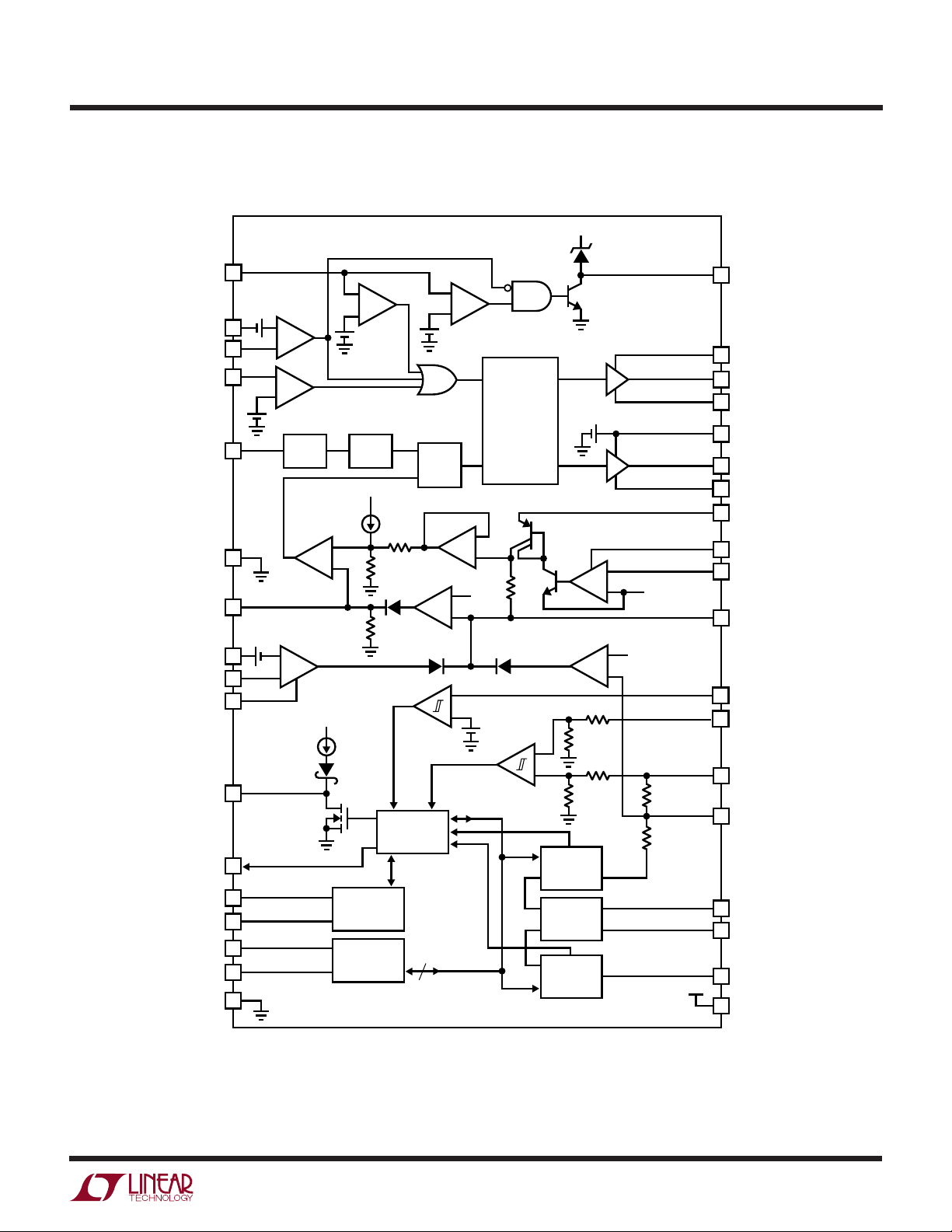
BLOCK DIAGRA
7
UV
0.2V
31
BAT1
32
V
CC
5
SDB
4
SYNC
6
AGND
V
27
C
92mV
+
CLP
9
CLN
10
COMP1
11
INTB
13
CHGEN
12
THERM
19
20
RNR
SCL
15
SDA
14
DGND
18
W
1.3V
LTC1759
V
CC
8V
8
INFET
1
BOOST
TGATE
2
3
SW
GBIAS
34
35 BGATE
36
PGND
33
BOOSTC
30
SPIN
29
SENSE
28
PROG
21
DCDIV
22
DCIN
23
BAT2
V
26
SET
I
24
LIMIT
25
V
LIMIT
17
I
SET
V
16
DD
1759 F02
S
R
CA2
13
+
–
6.7V
Q
–
B1
+
–
+
–
PWR_FAIL
+
V
SHDN
REF
1V
PWM
LOGIC
1k
–
+
20k
65k
10-BIT
VOLTAGE
DAC
LIMIT
DECODER
10-BIT
CURRENT
DAC
8.9V
CA1
VA
290k
812.5k
+
–
–
BAT1
V
REF
+
612k
72k
+
SLOPE COMP
+
–
V
DD
10µA
THERMISTOR
DECODER
CONTROLLER
–
6.7V
200kHz
OSC
75k
AC_PRESENT
CHARGER
CONTROLLER
SMBus
+
–
–
+
ONE
SHOT
C1
+
CL1
–
Figure 2
9
 Loading...