

Linear Technology LTC1758-1EMS8 Datasheet
250kHz Control Loop Bandwidth and
FEATURES
■
Dual Band RF Power Amplifier Control (LTC1758-2)
■
Internal Schottky Diode Detector with Improved
Dynamic Range vs LTC1757A
■
Wide Input Frequency Range: 850MHz to 2GHz
■
Autozero Loop Cancels Offset Errors and
Temperature Dependent Offsets
■
Wide VIN Range: 2.7V to 6V
Allows Direct Connection to Battery
■
RF Output Power Set by External DAC
■
250kHz Control Loop Bandwidth
■
Fast Acquire After Transmit Enable
■
Internal Frequency Compensation
■
Rail-to-Rail Power Control Outputs
■
Power Control Signal Overvoltage Protection
■
Low Operating Current: 1mA
■
Very Low Shutdown Current: <1µA
■
Available in 8-Pin MSOP (LTC1758-1)
and 10-Pin MSOP (LTC1758-2) Packages
■
Pin Compatible with LTC1757A-X
■
Improved Start Voltage Accuracy
■
Improved PCTL Input Filtering
U
APPLICATIO S
■
Single and Dual Band GSM/GPRS Cellular Telephones
■
PCS Devices
■
Wireless Data Modems
■
U.S. TDMA Cellular Phones
LTC1758-1/LTC1758-2
RF Power Controllers with
40dB Dynamic Range
U
DESCRIPTIO
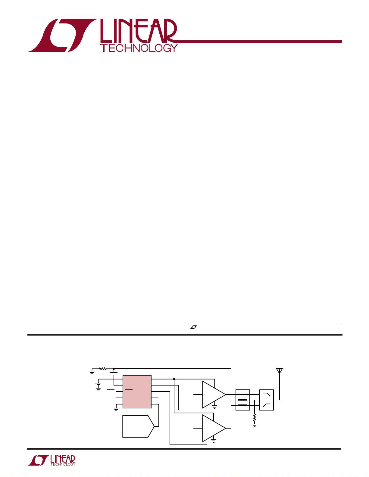
The LTC®1758-2 is a dual band RF power controller for
RF power amplifiers operating in the 850MHz to 2GHz
range. The loop bandwidth reduction to 250kHz improves frequency stability when controlling slow turn-on
PAs such as the Philips BGY280, Conexant RM009/
CX77302, Anadigics AWT6102/AWT6107 and the Hitachi
PF08107/PF08123B.
The LTC1758-1 is a single output RF power controller
that is identical in performance to the LTC1758-2 except
that one output (V
be used to drive a single RF or dual channel module with
integral multiplexer. This part is available in an 8-pin
MSOP package.
RF power is controlled by driving the RF amplifier power
control pins and sensing the resultant RF output power
via a directional coupler. The RF sense voltage is peak
detected using an on-chip Schottky diode. This detected
voltage is compared to the DAC voltage at the PCTL pin
to control the output power. The RF power amplifier is
protected against high supply current and high power
control pin voltages.
Internal and external offsets are cancelled over temperature by an autozero control loop, allowing accurate low
power programming. The shutdown feature disables the
part and reduces the supply current to <1µA.
, LTC and LT are registered trademarks of Linear Technology Corporation.
) is provided. The LTC1758-1 can
PCA
TYPICAL APPLICATIO
68Ω
33pF
V
IN
Li-Ion
SHDN
BSEL
U
LTC1758-2 Dual Band Cellular Telephone Transmitter
LTC1758-2
1
V
IN
2
RF
3
SHDN
4
BSEL
5
GND
DAC
V
V
PCA
V
PCB
TXEN
PCTL
10
CC
9
8
7
TXEN
6
900MHz
1.8GHz/1.9GHz RF PA
RF PA
DIRECTIONAL
COUPLER
DIPLEXER
50Ω
1758 TA01
1
LTC1758-1/LTC1758-2
1
2
3
4
5
V
IN
RF
SHDN
BSEL
GND
10
9
8
7
6
V
CC
V
PCA
V
PCB
TXEN
PCTL
TOP VIEW
MS10 PACKAGE
10-LEAD PLASTIC MSOP
WWWU
ABSOLUTE AXI U RATI GS
(Note 1)
VIN to GND............................................... –0.3V to 6.5V
V
, V
PCA
Voltage ..................................... – 0.3V to 3V
PCB
PCTL Voltage ............................... –0.3V to (VIN + 0.3V)
RF Voltage ........................................ (VIN – 2.2V) to 7V
I
, Continuous....................................................... 1A
VCC
I
, 12.5% Duty Cycle.......................................... 2.5A
VCC
SHDN, TXEN, BSEL
Voltage to GND ............................ –0.3V to (VIN + 0.3V)
UU
W
PACKAGE/ORDER I FOR ATIO
TOP VIEW
V
1
IN
2
RF
3
SHDN
4
GND
MS8 PACKAGE
8-LEAD PLASTIC MSOP
T
= 125°C, θJA = 160°C/W
JMAX
Consult LTC Marketing for parts specified with wider operating temperature ranges.
8
7
6
5
V
CC
V
PCA
TXEN
PCTL
ORDER PART
NUMBER
LTC1758-1EMS8
MS8 PART MARKING
LTSL
I
, 25% Duty Cycle ...................................... 20mA
VPCA/B
Operating Temperature Range (Note 2) . –30°C to 85°C
Storage Temperature Range ................ –65°C to 150°C
Maximum Junction Temperature ........................ 125°C
Lead Temperature (Soldering, 10 sec)................ 300°C
ORDER PART
NUMBER
LTC1758-2EMS
T
= 125°C, θJA = 160°C/W
JMAX
MS10 PART MARKING
LTSM
ELECTRICAL CHARACTERISTICS
The ● denotes specifications which apply over the full operating
temperature range, otherwise specifications are at TA = 25°C. VIN = 3.6V, SHDN = TXEN = HI, unless otherwise noted.
PARAMETER CONDITIONS MIN TYP MAX UNITS
VIN Operating Voltage ● 2.7 6 V
I
Shutdown Current SHDN = LO, TXEN = LO, BSEL = LO ● 1 µA
VIN
I
Autozero Current SHDN = HI, TXEN = LO ● 1 1.6 mA
VIN
I
Operating Current SHDN = HI, TXEN = HI, I
VIN
I
Current Limit 2.2 A
VCC
VIN to VCC Resistance SHDN = LO, TXEN = LO 90 150 mΩ
V
PCA/B VOL
V
Dropout Voltage I
PCA/B
V
Voltage Clamp R
PCA/B
V
Output Current V
PCA/B
V
Enable Time V
PCA/B
V
Bandwidth C
PCA/B
V
Load Capacitance (Note 6) 100 pF
PCA/B
V
Slew Rate V
PCA/B
V
Droop VIN = 2.7V, V
PCA/B
V
TXEN Start Voltage Open Loop, TXEN Low to High, C
PCA/B
SHDN Input Threshold VIN = 2.7V to 6V, TXEN = LO ● 0.35 1.4 V
TXEN, BSEL Input Threshold VIN = 2.7V to 6V ● 0.35 1.4 V
2
TXEN = HI, Open Loop, PCTL = –100mV ● 0 0.1 V
= 5.5mA, VIN = 2.7V ● VIN – 0.28 V
LOAD
= 400Ω, PCTL = 2V, External Gain = 0.417 ● 2.7 2.85 3.0 V
LOAD
= 2.4V, VIN = 2.7V ● 5.5 9 mA
PCA/B
V
= 2.6V, VIN = 3V ● 610 mA
PCA/B
= 2V Step, C
PCTL
= 100pF, R
LOAD
= 2V Step, C
PCTL
LOAD
LOAD
LOAD
= 2V Step ±1 µV/ms
PCTL
= I
VPCA
= 100pF (Note 5) ● 620 1000 ns
= 400Ω (Note 8) ● 180 250 330 kHz
= 100pF (Note 3) ● 0.75 1.3 V/µs
= 0mA, V
VPCB
= 100pF (Note 9) 500 600 700 mV
LOAD
= HI 1.1 1.7 mA
PCA/B
LTC1758-1/LTC1758-2
LECTRICAL C CHARA TERIST
E
ICS
The ● denotes specifications which apply over the full operating
temperature range, otherwise specifications are at TA = 25°C. VIN = 3.6V, SHDN = TXEN = VIN, unless otherwise noted.
PARAMETER CONDITIONS MIN TYP MAX UNITS
SHDN, TXEN, BSEL Input Current SHDN, TXEN or BSEL = 3.6V ● 10 25 50 µA
PCTL Input Voltage Control Range VIN = 3V to 6V, R
PCTL Input Voltage Range VIN = 3V, R
LOAD
PCTL Input Resistance SHDN = LO, TXEN = LO ● 50 90 140 kΩ
PCTL Input Filter 350 kHz
Autozero Range VIN = 2.7V, R
Autozero Settling Time (tS)t
, Shutdown to Enable (Autozero), VIN = 2.7V (Note 10) ● 50 µs
S
RF Input Frequency Range (Note 6) ● 850 2000 MHz
RF Input Power Range 900MHz (Note 6) –26 16 dBm
1800MHz (Note 6) –24 16 dBm
RF Input Impedance Referenced to VIN, SHDN = LO, TXEN = LO ● 100 200 350 Ω
BSEL Timing t1, Setup Time Prior to TXEN Asserted High 200 ns
, Hold Time After TXEN is Asserted Low 200 ns
t
2
Note 1: Absolute Maximum Ratings are those values beyond which the life
of a device may be impaired.
Note 2: The LTC1758-1 and LTC1758-2 are guaranteed to meet
performance specifications from 0°C to 70°C. Specifications over the
–30°C to 85°C operating temperature range are assured by design,
characterization and correlation with statistical process controls.
Note 3: Slew rate is measured open loop. The slew time at V
measured between 1V and 2V.
Note 4: Maximum DAC zero-scale offset voltage that can be applied to
PCTL.
= 400Ω ● 02V
LOAD
= 400Ω (Note 7) ● 2.4 V
= 400Ω (Note 4) ● 400 mV
LOAD
Note 5: This is the time from TXEN rising edge 50% switch point to
V
= 1V.
PCA/B
Note 6: Guaranteed by design. This parameter is not production tested.
Note 7: Includes maximum DAC offset voltage and maximum control
voltage.
Note 8: Bandwidth is calculated using the 10% to 90% rise time:
or V
PCB
is
BW = 0.35/rise time
PCA
Note 9: Measured 1µs after TXEN = HI.
Note 10: 50% switch point, SHDN HI = V
, TXEN HI = VIN.
IN
UW
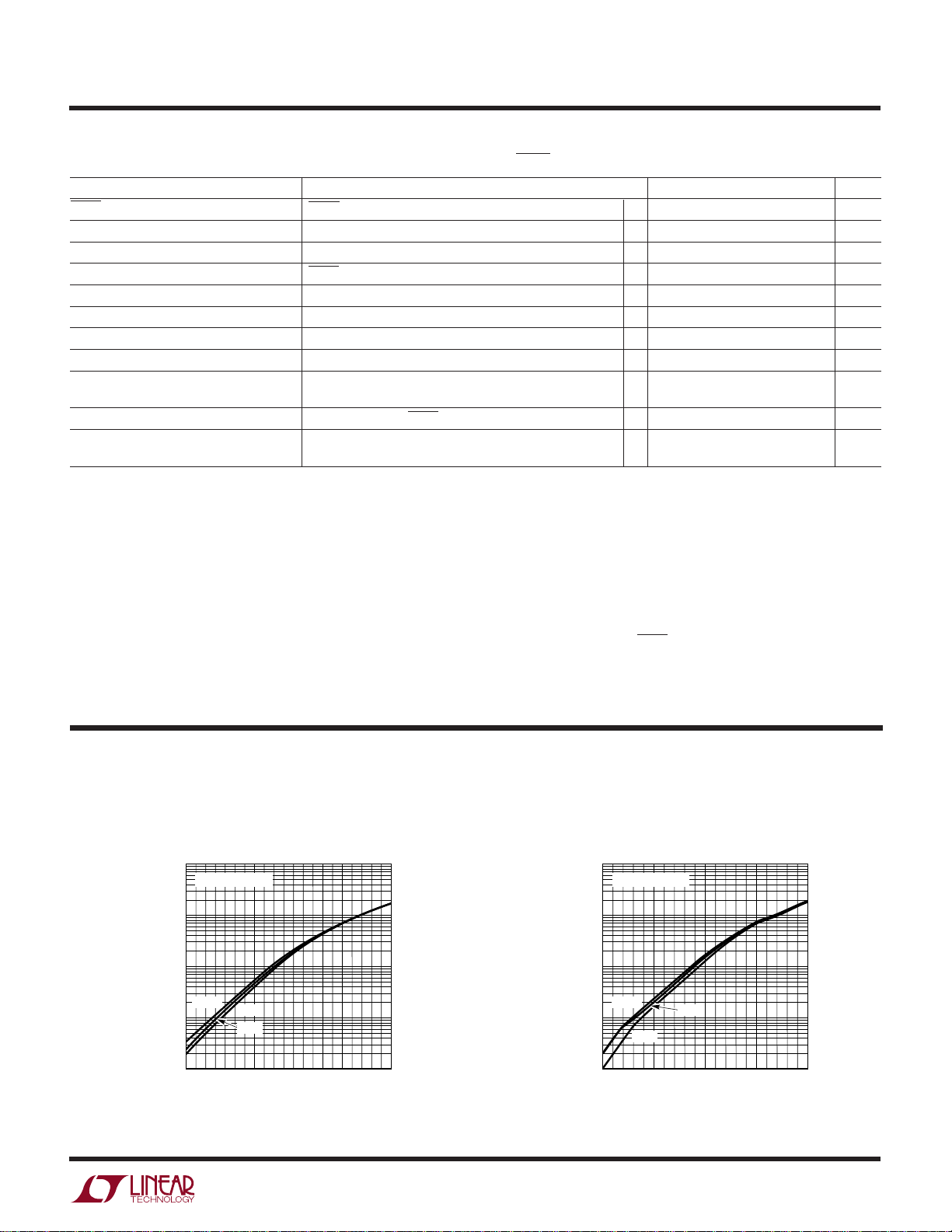
TYPICAL PERFOR A CE CHARACTERISTICS
RF Detector Characteristics
at 900MHz
10000
VIN = 3V TO 4.4V
1000
100
–30°C
10
1
–26 –14 –8 –2 4 10
PCTL REFERENCED DETECTOR OUTPUT VOLTAGE (mV)
75°C
25°C
–20
RF INPUT POWER (dBm)
16
1758 G01
RF Detector Characteristics
at 1800MHz
10000
VIN = 3V TO 4.4V
1000
100
–30°C
10
1
–24 –16 –12 –8 –4 0 4 8
PCTL REFERENCED DETECTOR OUTPUT VOLTAGE (mV)
–20
25°C
75°C
12 16
RF INPUT POWER (dBm)
1758 G02
3

LTC1758-1/LTC1758-2
U
PI FU CTIO S
VIN (Pin 1): Input Supply Voltage, 2.7V to 6V. VIN should
be bypassed with 0.1µF and 100pF ceramic capacitors.
Used as return for RF 200Ω termination.
RF (Pin 2): RF Feedback Voltage from the Directional
Coupler. Referenced to VIN. A coupling capacitor of 33pF
must be used to connect to the ground referenced directional coupler. The frequency range is 850MHz to 2000MHz.
This pin has an internal 200Ω termination, an internal
Schottky diode detector and peak detector capacitor.
SHDN (Pin 3): Shutdown Input. A logic low on the SHDN
pin places the part in shutdown mode. A logic high places
the part in autozero when TXEN is low. SHDN has an internal 150k pull-down resistor to ensure that the part is in shutdown when the drivers are in a three-state condition.
BSEL (Pin 4): (LTC1758-2 Only) Selects V
and V
resistor to ground.
GND (Pin 5/Pin 4): System Ground.
PCTL (Pin 6/Pin 5): Analog Input. The external power
control DAC drives this input. The amplifier servos the RF
when high. This input has an internal 150k
PCB
UU
(LTC1758-2/LTC1758-1)
when low
PCA
power until the RF detected signal equals the DAC signal.
The input impedance is typically 90kΩ.
TXEN (Pin 7/Pin 6): Transmit Enable Input. A logic high
enables the control amplifier. When TXEN is low and
SHDN is high the part is in the autozero mode. This input
has an internal 150k resistor to ground.
V
(Pin 8): (LTC1758-2 Only) Power Control Voltage
PCB
Output. This pin drives an external RF power amplifier
power control pin. The maximum load capacitance is
100pF. The output is capable of rail-to-rail swings at low
load currents. Selected when BSEL is high.
V
(Pin 9/Pin 7): Power Control Voltage Output. This pin
PCA
drives an external RF power amplifier power control pin.
The maximum load capacitance is 100pF. The output is
capable of rail-to-rail swings at low load currents. Selected
when BSEL is low (LTC1758-2 only).
VCC (Pin 10/Pin 8): RF Power Amplifier Supply. This pin
has an internal 0.090Ω sense resistor between VIN and
VCC that senses the RF power amplifier supply current to
detect overcurrent conditions.
4
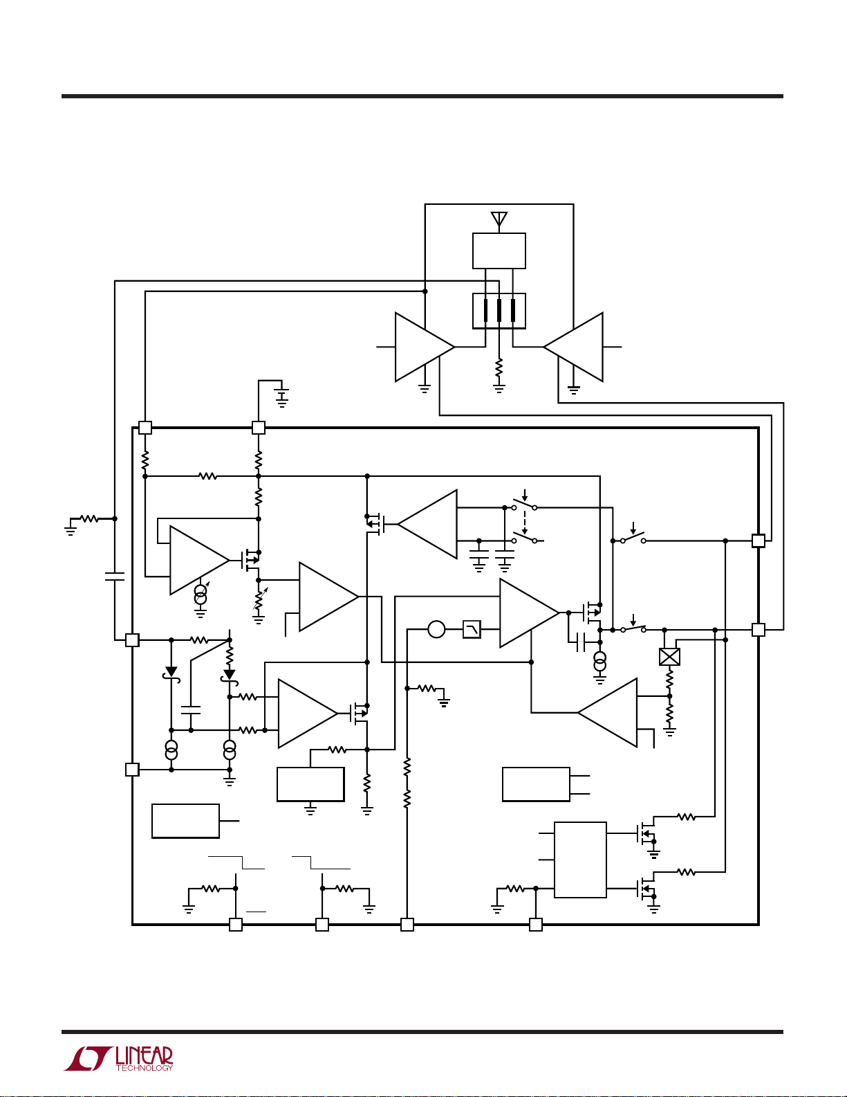
BLOCK DIAGRA
LTC1758-1/LTC1758-2
W
(LTC1758-2)
DIPLEXER
68Ω
33pF
10
V
CC
R
SENSE
0.02Ω 0.02Ω
0.05Ω
METAL
–
CS
+
OFFSET
TRIM
V
IN
RF
2
GND
5
200Ω
28pF
60µA60µA
BG1
THERMAL
SHUTDOWN
OPERATE SHDN
1
V
100Ω
METAL
OVERCURRENT
PROGRAMMABLE
200Ω
35k
35k
TSDB
Li-Ion
IN
GAIN
TRIM
+
RFDET
–
COMPRESSION
XMT AUTOZERO
RF PA900MHz
50Ω
AUTOZERO
TXENB
–
AZ
+
g
m
50mV FILTER
+
–
ICL
33k
22k
33k
22k
22k
+
CAMP
–
BG1
1.2V BANDGAP
TXENI
150k150k150k
RF PA
ADJUSTABLE
C
C
VPC
MUX
CONTROL
1.8GHz/1.9GHz
400µA
g
m
1.2V
ADJUSTABLE
PB
PA
PA
V
PCA
9
PB
140k
110k
1.2V
12Ω
100ΩTSDB
12Ω
100Ω
V
PCB
8
SHDN
TXEN
73
PCTL
6
BSEL
4
1758 BD
5
 Loading...