

Linear Technology LTC1756 Datasheet
FEATURES
Final Electrical Specifications
LTC1756
Smart Card Interface
February 2000
U
DESCRIPTION
■
Fully ISO 7816-3 and EMV Compliant
■
Buck-Boost Charge Pump Generates 3V or 5V
■
2.7V to 5.5V Input Voltage Range
■
3V↔ 5V Signal Level Translator
■
>10kV ESD on All Smart Card Pins
■
Dynamic Pull-Ups Deliver Fast Signal Rise Times
■
Soft Start Limits Inrush Current at Turn On
■
Very Low Operating Current: 75µA
■
Shutdown Current: <2.5µA
■
Short-Circuit and Overtemperature Protected
■
Available in 16-Pin SSOP Package
U
APPLICATIONS
■
Handheld Payment Terminals
■
Pay Telephones
■
ATMs
■
Key Chain Readers
■
Smart Card Readers
The LTC®1756 universal Smart Card interface is fully
compliant with ISO 7816-3 and EMV specifications. It
provides the smallest and simplest interface circuit between a host microcontroller and general purpose Smart
Cards.
An internal charge pump DC/DC converter delivers regulated 3V or 5V to the Smart Card, while an on-chip level
shifter allows a connection to a low voltage controller. All
Smart Card contacts are rated for 10kV ESD, eliminating
the need for external ESD protection devices.
Input voltage may range from 2.7V to 5.5V, allowing direct
connection to a battery. Automatic DC/DC converter soft
start mitigates start-up problems that may result when the
input power is provided by another regulator.
Battery life is maximized by 75µA operating current and
2µA shutdown current. The 16-pin SSOP package mini-
mizes PCB area for compact portable systems.
, LTC and LT are registered trademarks of Linear Technology Corporation.
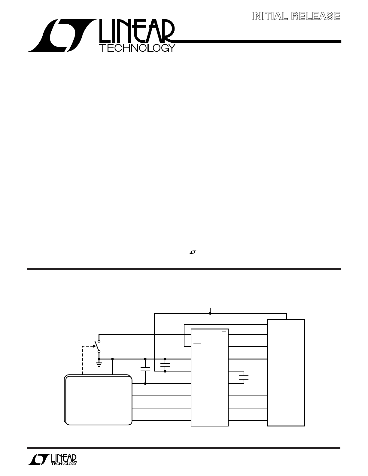
TYPICAL APPLICATION
SMART CARD
PRESENT SWITCH
N.O.
GND
SMART CARD
V
I/O
RST
CLK
U
CC
10µF
3.3V
1
PRES
2
PWR
3
C3
C2
10µF
GND
4
V
IN
LTC1756
5
V
CC
6
I/O
7
RST
8
CLK
5V/3V
CARD
READY
DATA
RIN
CIN
16
15
14
13
–
C
12
+
C
11
10
9
C1
0.68µF
µCONTROLLER
1756 TA01
Information furnished by Linear Technology Corporation is believed to be accurate and reliable.
However, no responsibility is assumed for its use. Linear Technology Corporation makes no representation that the interconnection of its circuits as described herein will not infringe on existing patent rights.
1
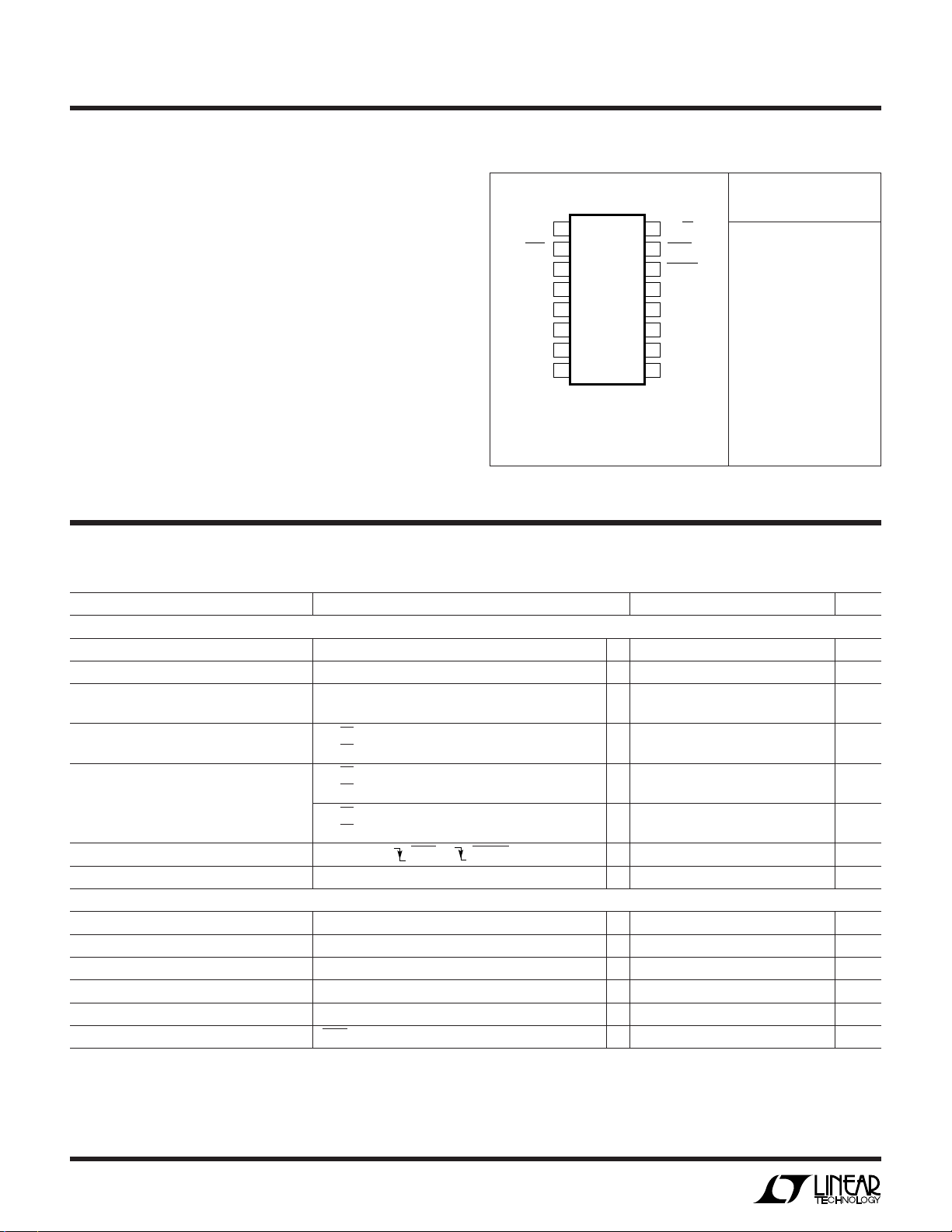
LTC1756
GN PACKAGE
16-LEAD NARROW PLASTIC SSOP
1
2
3
4
5
6
7
8
TOP VIEW
16
15
14
13
12
11
10
9
PRES
PWR
GND
V
IN
V
CC
I/O
RST
CLK
5V/3V
CARD
READY
C
–
C
+
DATA
RIN
CIN
WW
W
ABSOLUTE MAXIMUM RATINGS
U
PACKAGE
/
O
RDER I FOR ATIO
(Note 1)
VIN to GND............................................... –0.3V to 6.0V
VCC to GND .............................................. –0.3V to 5.5V
Digital Inputs to GND..................... –0.3V to VIN + 0.3V
CLK, RST, I/O to GND .....................–0.3V to VCC + 0.3V
VCC Short-Circuit Duration............................... Indefinite
Operating Temperature Range (Note 2) .. –40°C to 85°C
Storage Temperature Range ................ – 65°C to 150°C
Lead Temperature (Soldering, 10 sec)................. 300°C
T
= 125°C, θJA = 135°C/W
JMAX
Consult factory for Industrial and Military grade parts.
ELECTRICAL CHARACTERISTICS
temperature range, otherwise specificatons are at TA = 25°C. VIN = 2.7V to 5.5V, unless otherwise noted.
The ● denotes specifications which apply over the full specified
WU
ORDER PART
NUMBER
LTC1756EGN
U
PARAMETER CONDITIONS MIN TYP MAX UNITS
Power Supply
VIN Operating Voltage ● 2.7 5.5 V
I
Operating Current ACTIVE State, I
VIN
I
Shutdown Current IDLE State, VIN ≤ 3.6V ● 2.5 µA
VIN
VCC Output Voltage 5V/3V = V
I
Output Current 5V/3V = 0V 3V ≤ VIN ≤ 5.5V ● 55 mA
VCC
VCC Turn-On Time C
VCC Discharge Time to 0.4V I
Controller Input/Output DATA
High Input Voltage Threshold (VIH) ● VIN – 0.6 0.5 • V
Low Input Voltage Threshold (VIL) ● 0.5 • V
High Level Output Voltage (VOH) Source Current = 20µA ● 0.7 • V
Low Level Output Voltage (VOL) Sink Current = –500µA (Note 3) ● 0.3 V
Output Rise/Fall Time Loaded with 30pF, 10% to 90% ● 0.5 µs
Input Current (IIH/IIL) PWR = V
2
= 0 ● 75 150 µA
VCC
IDLE State, 3.6V ≤ V
5V/3V = 0V
5V/3V = V
5V/3V = 0V 2.7V ≤ VIN ≤ 5.5V ● 55 mA
5V/3V = V
VCC
IN
IN
IN
= 10µF, PWR to READY ● 2.7 12 ms
OUT
= 0mA, VCC = 5V, C
IN
≤ 5.5V ● 10 µA
IN
● 4.75 5.00 5.25 V
● 2.80 3.00 3.20 V
3V ≤ VIN ≤ 5.5V ● 65 mA
2.7V ≤ VIN ≤ 5.5V ● 40 mA
= 10µF ● 100 250 µs
OUT
IN
0.3 V
IN
IN
● –1 1 µA
V
V
LTC1756
ELECTRICAL CHARACTERISTICS
The ● denotes specifications which apply over the full specified
temperature range, otherwise specificatons are at TA = 25°C. VIN = 2.7V to 5.5V, unless otherwise noted.
PARAMETER CONDITIONS MIN TYP MAX UNITS
RIN, CIN, PWR, 5V/3V
High Input Voltage Threshold (VIH) ● 0.7 • VIN0.5 • V
Low Input Voltage Threshold (VIL) ● 0.5 • VIN0.2 • V
Input Current (IIH/IIL) ● –1 1 µA
READY, CARD
Pull-Up Current (IOH) ● 250 nA
Low Level Output Voltage (VOL) Sink Current = –20µA ● 0.3 V
Smart Card Input/Output I/O, VCC = 3V or 5V
High Input Voltage Threshold (VIH)I
Low Input Voltage Threshold (VIL)I
High Level Output Voltage (VOH) Source Current = 20µA, DATA = V
Low Level Output Voltage (VOL) Sink Current = –1mA, DATA = 0V (Note 3) ● 0.3 V
Rise/ Fall Time Loaded with 30pF, 10% to 90% ● 0.5 µs
Short-Circuit Current Shorted to V
CLK
High Level Output Voltage (VOH) Source Current = 100µA ● VCC – 0.5 V
Low Level Output Voltage (VOL) Sink Current = –200µA ● 0.3 V
CLK Rise/Fall Time CLK Loaded with 30pF ● 16 ns
CLK Frequency CLK Loaded with 30pF ● 5 MHz
RST
High Level Output Voltage (VOH) Source Current = 200µA ● 0.8 • V
Low Level Output Voltage (VOL) Sink Current = –200µA ● 0.3 V
RST Rise/Fall Time Loaded with 30pF ● 0.5 µs
PRES
High Input Voltage Threshold (VIH) ● 0.7 • VIN0.5 • V
Low Input Voltage Threshold (VIL) ● 0.5 • VIN0.2 • V
PRES Pull-Up Current V
PRES Debounce Time Proportional to the 0.68µF Charge Pump Capacitor ● 40 80 ms
= ±20µA ● 0.6 • VCC0.5 • V
IH(MAX)
= 1mA ● 0.5 • V
IL(MAX)
IN
CC
= 0V ● 0.5 1 µA
PRES
● 0.8 • V
● 3.5 5 mA
CC
CC
IN
CC
CC
IN
IN
0.8 V
IN
V
V
V
V
V
V
V
Note 1: Absolute Maximum Ratings are those values beyond which the life
of a device may be impaired.
Note 2: The LTC1756 is guaranteed to meet performance specifications
from 0°C to 70°C. Specifications over the –40°C to 85°C operating
temperature range are assured by design, characterization and correlation
with statistical process controls.
Note 3: The DATA and I/O pull-down drivers must sink up to 250µA
sourced by the internal current sources.
3
LTC1756
UUU
PIN FUNCTIONS
PRES (Pin 1): (Input) Connects to the Smart Card acceptor’s
PRESENT indicator switch to detect if a card is inserted.
This pin has a pull-up current source so that a normally
open grounded switch can be detected with no external
components. The pull-up current source is nonlinear,
delivering higher current when the PRES pin is above 1V
but very little current below 1V. This helps resist false card
indications due to leakage current.
PWR (Pin 2): (Input) A low on the PWR pin places the
LTC1756 in the ACTIVE state enabling the charge pump.
The READY pin indicates when the card supply voltage
(VCC) has reached its final value and communication with
the Smart Card is possible. The reset and clock channels
are enabled after READY goes low. The I/O channel is also
enabled only after READY goes low.
The falling edge of PWR latches the state of the 5V/3V pin.
After PWR is low, changes on the 5V/3V pin are ignored.
GND (Pin 3): Ground Reference for the IC. This pin should
be connected to a low impedance ground plane. Bypass
capacitors for VIN and VCC should be in close proximity to
the GND pin.
VIN (Pin 4): Supply Voltage. May be between 2.7V and 5.5V.
A 10µF low ESR ceramic bypass capacitor is required on
this pin for optimum performance.
VCC (Pin 5): Regulated Smart Card Supply Voltage. This
pin should be connected to the Smart Card VCC contact.
The 5V/3V pin determines the VCC output voltage.
The VCC pin is protected against short circuits by comparing the actual output voltage with an internal reference
voltage. If VCC is below its correct level (for as little as 5µs)
the LTC1756 switches to the Alarm state (see the State
Diagram). The VCC pin requires a 10µF charge storage
capacitor to ground. For optimum performance a low ESR
ceramic capacitor should be used.
to the Smart Card I/O contact. The Smart Card I/O pin must
be able to sink up to 250µA when driving the I/O pin low
due to the pull-up current source. The I/O pin becomes a
low impedance to ground during the Idle state. It does not
become active until READY goes low indicating that VCC is
stable.
Once READY is low, the I/O pin is protected against short
circuits to VCC by current limiting to 5mA maximum.
The DATA-I/O channel is bidirectional for half-duplex
transmissions. Its idle state is H-H. Once an L is detected
on one side of the channel the direction of transmission is
established. Specifically, the side which received an L first
is now the input, and the opposite side is the output.
Transmission from the output side back to the input side
is inhibited, thereby preventing a latch condition. Once the
input side releases its L, both sides return to H, and the
channel is now ready for a new L to be transmitted in either
direction. If an L is forced externally on the output side, and
it persists until after the L on the input side is released, this
illegal input will not be transmitted to the input side
because the transmission direction will not have changed.
The direction of transmission can only be established from
the idle (H-H) state and is determined by the first receipt
of an L on either side.
RST (Pin 7): (Output) Level-Shifted Reset Output Pin. This
pin should be connected to the Smart Card RST contact.
The RST pin becomes a low impedance to ground during
the Idle state (see the State Diagram). The reset channel
does not become active until the READY signal goes low
indicating that VCC is stable.
Short-circuit protection is provided on the RST pin by
comparing RST with RIN. If these signals differ for several
microseconds then the LTC1756 switches to the Alarm
state. This fault checking is only performed after the VCC pin
has reached its final value (as indicated by the READY pin).
During the Idle and Alarm states the VCC pin is rapidly
discharged to ground to comply with the deactivation
requirements of the EMV and ISO-7816 specifications.
I/O (Pin 6): (Input/Output) Smart Card Side Data I/O Pin.
This pin is used for bidirectional data transfer between the
microcontroller and the Smart Card. It should be connected
4
CLK (Pin 8): (Output) Level-Shifted Clock Output Pin. This
pin should be connected to the Smart Card CLK contact.
The CLK pin becomes a low impedance to ground during
the Idle state (see the State Diagram). The clock channel
does not become active until the READY signal goes low
indicating that VCC is stable.
 Loading...