

Linear Technology LTC1735 Datasheet
FEATURES
LTC1735
High Efficiency
Synchronous Step-Down
Switching Regulator
U
DESCRIPTIO
■
Dual N-Channel MOSFET Synchronous Drive
■
Synchronizable/Programmable Fixed Frequency
■
Wide VIN Range: 3.5V to 36V Operation
■
V
Range: 0.8V to 6V
OUT
■
OPTI-LOOPTM Compensation Minimizes C
■
±
1% Output Voltage Accuracy
■
Internal Current Foldback
■
Output Overvoltage Crowbar Protection
■
Latched Short-Circuit Shutdown Timer
OUT
with Defeat Option
■
Very Low Dropout Operation: 99% Duty Cycle
■
Forced Continuous Control Pin
■
Optional Programmable Soft-Start
■
Remote Output Voltage Sense
■
Logic Controlled Micropower Shutdown: IQ < 25µA
■
LTC1435 Pin Compatible with
Minor Component Changes
■
Available in 16-Lead Narrow SSOP and SO Packages
U
APPLICATIO S
■
Notebook and Palmtop Computers, PDAs
■
Cellular Telephones and Wireless Modems
■
DC Power Distribution Systems
The LTC®1735 is a synchronous step-down switching
regulator controller that drives external N-channel power
MOSFETs using a fixed frequency architecture. Burst
ModeTM operation provides high efficiency at low load
currents. The precision 0.8V reference is compatible with
future microprocessor generations. OPTI-LOOP compensation allows the transient response to be optimized over
a wide range of output capacitance and ESR values.
The operating frequency (synchronizable up to 500kHz) is
set by an external capacitor allowing maximum flexibility
in optimizing efficiency. A forced continuous control pin
reduces noise and RF interference and can assist secondary winding regulation by disabling Burst Mode operation
when the main output is lightly loaded.
Protection features include internal foldback current limiting, output overvoltage crowbar and optional shortcircuit shutdown. Soft-start is provided by an external
capacitor that can be used to properly sequence supplies.
The operating current level is user-programmable via an
external current sense resistor. Wide input supply range
allows operation from 3.5V to 30V (36V maximum).
, LTC and LT are registered trademarks of Linear Technology Corporation.
Burst Mode and OPTI-LOOP are trademarks of Linear Technology Corporation.
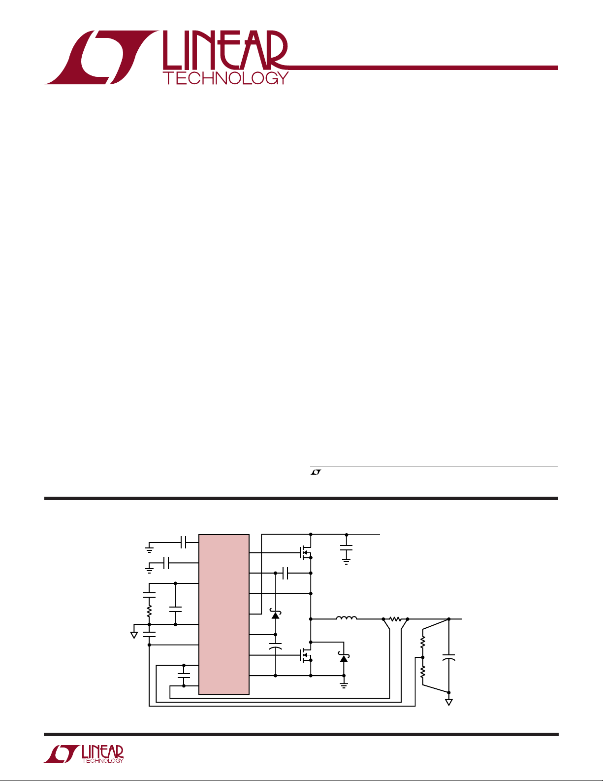
TYPICAL APPLICATIO
C
OSC
47pF
C
SS
0.1µF
C
C
330pF
C
100pF
1000pF
C
100pF
R
33k
U
C
OSC
RUN/SS
I
TH
C2
SGND
V
OSENSE
SENSE
SENSE
LTC1735
–
+
BOOST
INTV
PGND
TG
SW
V
IN
CC
BG
C
0.22µF
D
CMDSH-3
+
4.7µF
Figure 1. High Efficiency Step-Down Converter
M1
FDS6680A
B
B
M2
FDS6680A
L1
2µH
D1
MBRS340T3
V
IN
5V TO 24V
C
IN
22µF
50V
: PANASONIC EEFUEOG181R
C
OUT
: MARCON THCR70E1H226ZT
C
IN
L1: PANASONIC ETQP6FZR0HFA
R
SENSE
R
SENSE
0.005Ω
: IRC LRF2010-01-R005J
R1
20k
1%
R2
20k
1%
1735 F01
V
OUT
1.6V
9A
C
OUT
180µF
+
4V
×4
SP
1
LTC1735
WW
W
U
ABSOLUTE AXI U RATI GS
(Note 1)
Input Supply Voltage (VIN).........................36V to –0.3V
Topside Driver Supply Voltage (BOOST)....42V to –0.3V
Switch Voltage (SW) ....................................36V to – 5V
EXTVCC Voltage ...........................................7V to –0.3V
Boosted Driver Voltage (BOOST – SW) .......7V to –0.3V
SENSE+, SENSE– Voltages ..........1.1 (INTVCC) to –0.3V
FCB Voltage ............................(INTVCC + 0.3V) to –0.3V
ITH, V
OSENSE
RUN/SS Voltages.........................................7V to – 0.3V
Peak Driver Output Current <10µs (TG, BG) .............. 3A
INTVCC Output Current ......................................... 50mA
Operating Ambient Temperature Range
LTC1735C ............................................... 0°C to 85°C
LTC1735I............................................ –40°C to 85°C
Junction Temperature (Note 2).............................125°C
Storage Temperature Range ................. –65°C to 150°C
Lead Temperature (Soldering, 10 sec).................. 300°C
Voltages ...............................2.7V to –0.3V
UUW
PACKAGE/ORDER I FOR ATIO
TOP VIEW
1
C
OSC
2
RUN/SS
3
I
TH
4
FCB
5
SGND
6
V
OSENSE
–
7
SENSE
+
8
SENSE
GN PACKAGE
16-LEAD NARROW
PLASTIC SSOP
T
= 125°C, θJA = 130°C/W (GN)
JMAX
= 125°C, θJA = 110°C/W (S)
T
JMAX
Consult factory for Military grade parts.
16
TG
15
BOOST
14
SW
13
V
IN
12
INTV
CC
11
BG
10
PGND
9
EXTV
CC
S PACKAGE
16-LEAD PLASTIC SO
ORDER PART
NUMBER
LTC1735CGN
LTC1735CS
LTC1735IGN
LTC1735IS
GN PART MARKING
1735
1735I
ELECTRICAL CHARACTERISTICS
temperature range, otherwise specifications are at TA = 25°C. VIN = 15V, V
SYMBOL PARAMETER CONDITIONS MIN TYP MAX UNITS
Main Control Loop
I
VOSENSE
V
OSENSE
∆V
LINEREG
∆V
LOADREG
DF Max Maximum Duty Factor In Dropout 98 99.4 %
g
m
V
FCB
I
FCB
V
OVL
I
Q
V
RUN/SS
V
RUN/SS
I
RUN/SS
I
SCL
UVLO Undervoltage Lockout Measured at VIN Pin (VIN Ramping Down) ● 3.5 3.9 V
∆V
SENSE(MAX)
Feedback Current (Note 3) –4 –25 nA
Feedback Voltage (Note 3) ● 0.792 0.8 0.808 V
Reference Voltage Line Regulation VIN = 3.6V to 30V (Note 3) 0.001 0.02 %/V
Output Voltage Load Regulation (Note 3)
Transconductance Amplifier g
Forced Continuous Threshold ● 0.76 0.8 0.84 V
Forced Continuous Current V
Feedback Overvoltage Lockout ● 0.84 0.86 0.88 V
Input DC Supply Current (Note 4)
Normal Mode 450 µA
Shutdown V
Run Pin Start Threshold V
Run Pin Begin Latchoff Threshold V
Soft-Start Charge Current V
RUN/SS Discharge Current Soft Short Condition, V
Maximum Current Sense Threshold V
m
The ● denotes specifications which apply over the full operating
= 5V unless otherwise noted.
RUN/SS
Measured in Servo Loop; V
Measured in Servo Loop; V
= 0.85V – 0.17 –0.3 µA
FCB
= 0V 15 25 µA
RUN/SS
, Ramping Positive 1.0 1.5 1.9 V
RUN/SS
, Ramping Positive 4.1 4.5 V
RUN/SS
= 0V –0.7 – 1.2 µA
RUN/SS
= 4.5V
V
RUN/SS
= 0.7V ● 60 75 85 mV
OSENSE
= 0.7V ● 0.1 0.3 %
ITH
= 2V ● –0.1 –0.3 %
ITH
1.3 mmho
= 0.5V, 0.5 2 4 µA
OSENSE
2
LTC1735
ELECTRICAL CHARACTERISTICS
temperature range, otherwise specifications are at TA = 25°C. VIN = 15V, V
The ● denotes specifications which apply over the full operating
= 5V unless otherwise noted.
RUN/SS
SYMBOL PARAMETER CONDITIONS MIN TYP MAX UNITS
I
SENSE
t
ON(MIN)
Sense Pins Total Source Current V
SENSE
–
= V
Minimum On-Time Tested with a Square Wave (Note 6) 160 200 ns
+
= 0V 60 80 µA
SENSE
TG Transition Time: (Note 7)
TG t
TG t
r
f
Rise Time C
Fall Time C
= 3300pF 50 90 ns
LOAD
= 3300pF 50 90 ns
LOAD
BG Transition Time: (Note 7)
BG t
r
BG t
f
TG/BG t
Rise Time C
Fall Time C
1D
Top Gate Off to Synchronous C
= 3300pF 50 90 ns
LOAD
= 3300pF 40 80 ns
LOAD
= 3300pF Each Driver 100 ns
LOAD
Gate On Delay Time
TG/BG t
2D
Synchronous Gate Off to Top C
= 3300pF Each Driver 70 ns
LOAD
Gate On Delay Time
Internal VCC Regulator
V
INTVCC
V
LDO(INT)
V
LDO(EXT)
V
EXTVCC
V
EXTVCC(HYS)
Internal VCC Voltage 6V < VIN < 30V, V
Internal V
EXTVCC Drop Voltage ICC = 20mA, V
Load Regulation ICC = 0 to 20mA, V
CC
EXTVCC
= 4V 5.0 5.2 5.4 V
EXTVCC
= 4V 0.2 1 %
EXTVCC
= 5V 130 200 mV
EXTVCC Switchover Voltage ICC = 20mA, EXTVCC Ramping Positive ● 4.5 4.7 V
EXTVCC Hysteresis 0.2 V
Oscillator
f
OSC
fH/f
OSC
f
FCB(SYNC)
Oscillator Frequency C
= 43pF (Note 5) 265 300 335 kHz
OSC
Maximum Sync Frequency Ratio 1.3
FCB Pin Threshold For Sync Ramping Negative 0.9 1.2 V
Note 1: Absolute Maximum Ratings are those values beyond which the life
of a device may be impaired.
Note 2: T
dissipation P
LTC1735CS, LTC1735IS: T
is calculated from the ambient temperature TA and power
J
according to the following formulas:
D
= TA + (PD • 110 °C/W)
J
LTC1735CGN, LTC1735IGN: TJ = TA + (PD • 130°C/W)
Note 3: The LTC1735 is tested in a feedback loop that servos V
the balance point for the error amplifier (V
ITH
= 1.2V).
OSENSE
to
Note 4: Dynamic supply current is higher due to the gate charge being
delivered at the switching frequency. See Applications Information.
Note 5: Oscillator frequency is tested by measuring the C
current (I
) and applying the formula:
OSC
f
OSC
8 477 10
=
CpF I I
OSC CHG DIS
11
.( )
+
()
11
–
11
+
1
OSC
charge
Note 6: The minimum on-time condition corresponds to an inductor peakto-peak ripple current ≥40% of I
(see Minimum On-Time
MAX
Considerations in the Applications Information section).
Note 7: Rise and fall times are measured using 10% and 90% levels.
Delay times are measured using 50% levels.
3
LTC1735
UW
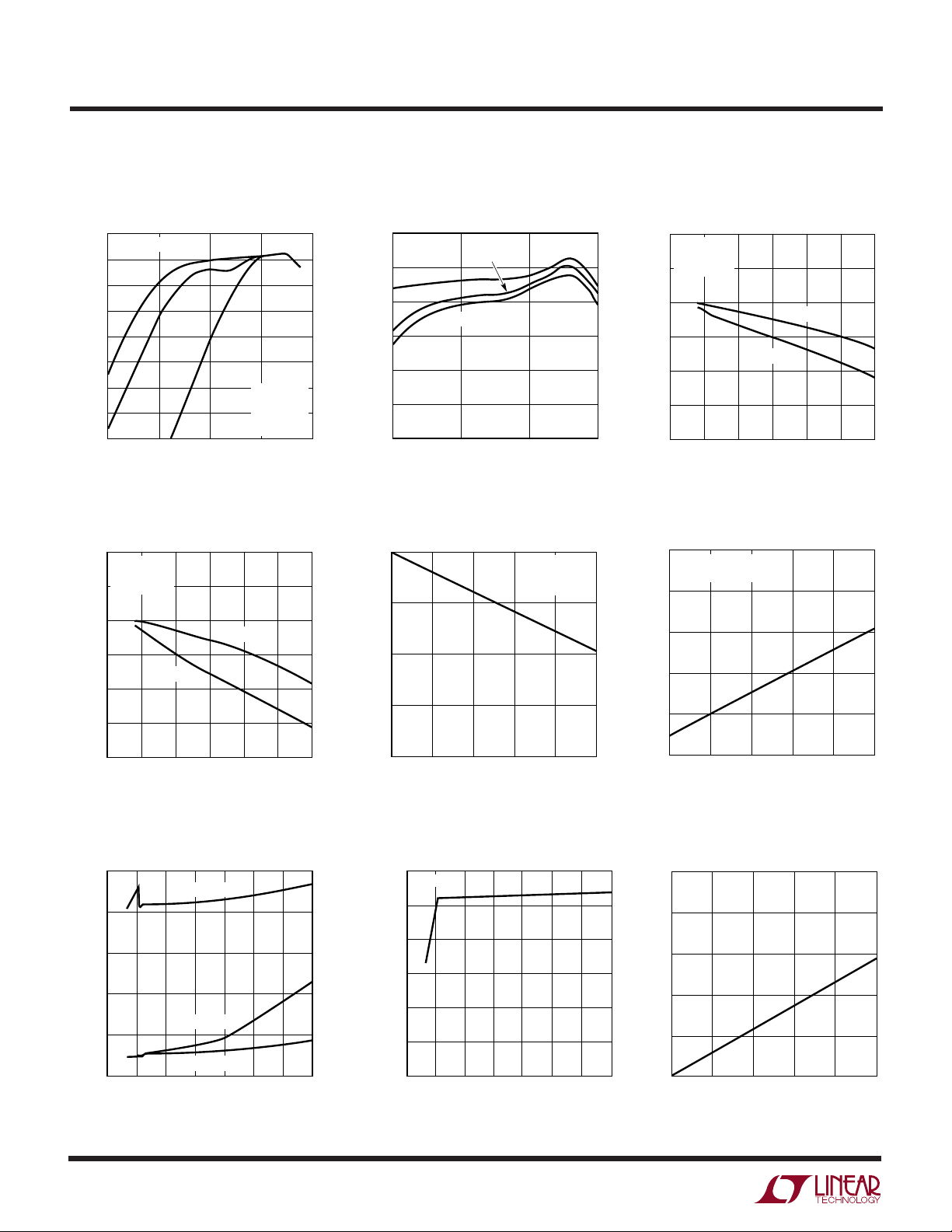
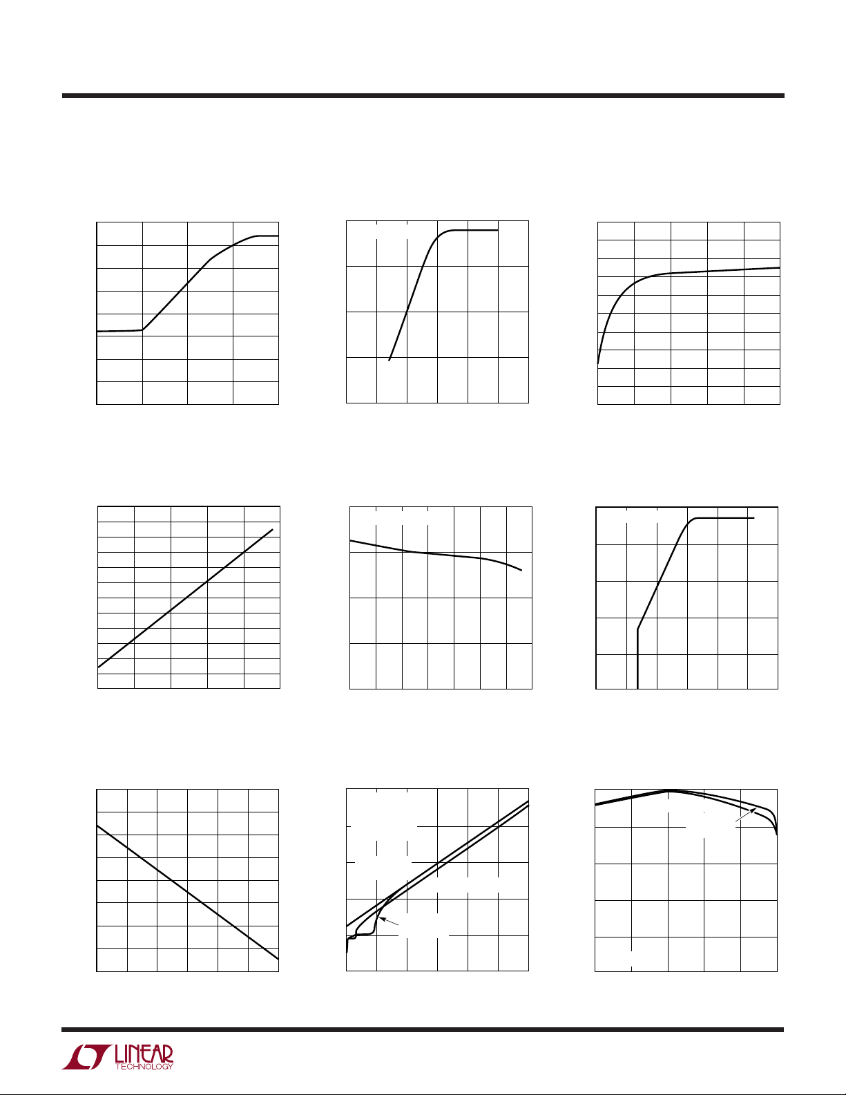
TYPICAL PERFOR A CE CHARACTERISTICS
Efficiency vs Load Current
(3 Operating Modes) Efficiency vs Load Current
100
EXTVCC OPEN
90
BURST
80
70
60
50
EFFICIENCY (%)
40
30
20
0.001
SYNC
0.01
0.1
LOAD CURRENT (A)
CONT
VIN = 10V
= 3.3V
V
OUT
R
= 0.01Ω
S
= 300kHz
f
O
1
10
1735 G01
100
EXTV
= 5V
CC
FIGURE 1
90
VIN = 5V
80
70
EFFICIENCY (%)
60
50
40
0.01 0.1 1 10
= 15V
V
IN
VIN = 24V
LOAD CURRENT (A)
1735 G02
Efficiency vs Input Voltage
100
EXTVCC = 5V
= 1.6V
V
OUT
95
FIGURE 1
90
85
I
EFFICIENCY (%)
80
75
70
0
5
OUT
10 15 20
INPUT VOLTAGE (V)
I
OUT
= 0.5A
= 5A
25 30
1735 G03
Efficiency vs Input Voltage
100
EXTVCC OPEN
= 1.6V
V
OUT
95
FIGURE 1
90
85
I
= 0.5A
EFFICIENCY (%)
80
75
70
OUT
0
10 15 20
5
INPUT VOLTAGE (V)
Input and Shutdown Currents
vs Input Voltage
500
EXTVCC OPEN
400
300
200
INPUT CURRENT (µA)
100
0
05
SHUTDOWN
EXTVCC = 5V
20
15
10
INPUT VOLTAGE (V)
I
OUT
= 5A
25
25 30
1735 G04
30
1735 G07
Load Regulation
0
–0.1
(%)
OUT
–0.2
NORMALIZED V
–0.3
–0.4
0
2
4
LOAD CURRENT (A)
VIN – V
vs Load Current
500
400
300
(mV)
OUT
– V
200
IN
V
100
R
SENSE
V
OUT
0
0
FCB = 0V
= 15V
V
IN
FIGURE 1
6
8
10
1735 G05
Dropout Voltage
OUT
= 0.005Ω
= 5V – 5% DROP
2468
LOAD CURRENT (A)
10
1735 G06
EXTVCC Switch Drop
INTVCC Line Regulation
100
SHUTDOWN CURRENT (µA)
80
60
40
20
0
35
6
1mA LOAD
5
4
3
VOLTAGE (V)
CC
2
INTV
1
0
0
510
INPUT VOLTAGE (V)
20 30 35
15 25
1735 G08
vs INTVCC Load Current
500
400
(mV)
300
CC
– INTV
200
CC
EXTV
100
0
10
0
INTVCC LOAD CURRENT (mA)
30
40
20
50
1735 G09
4
UW
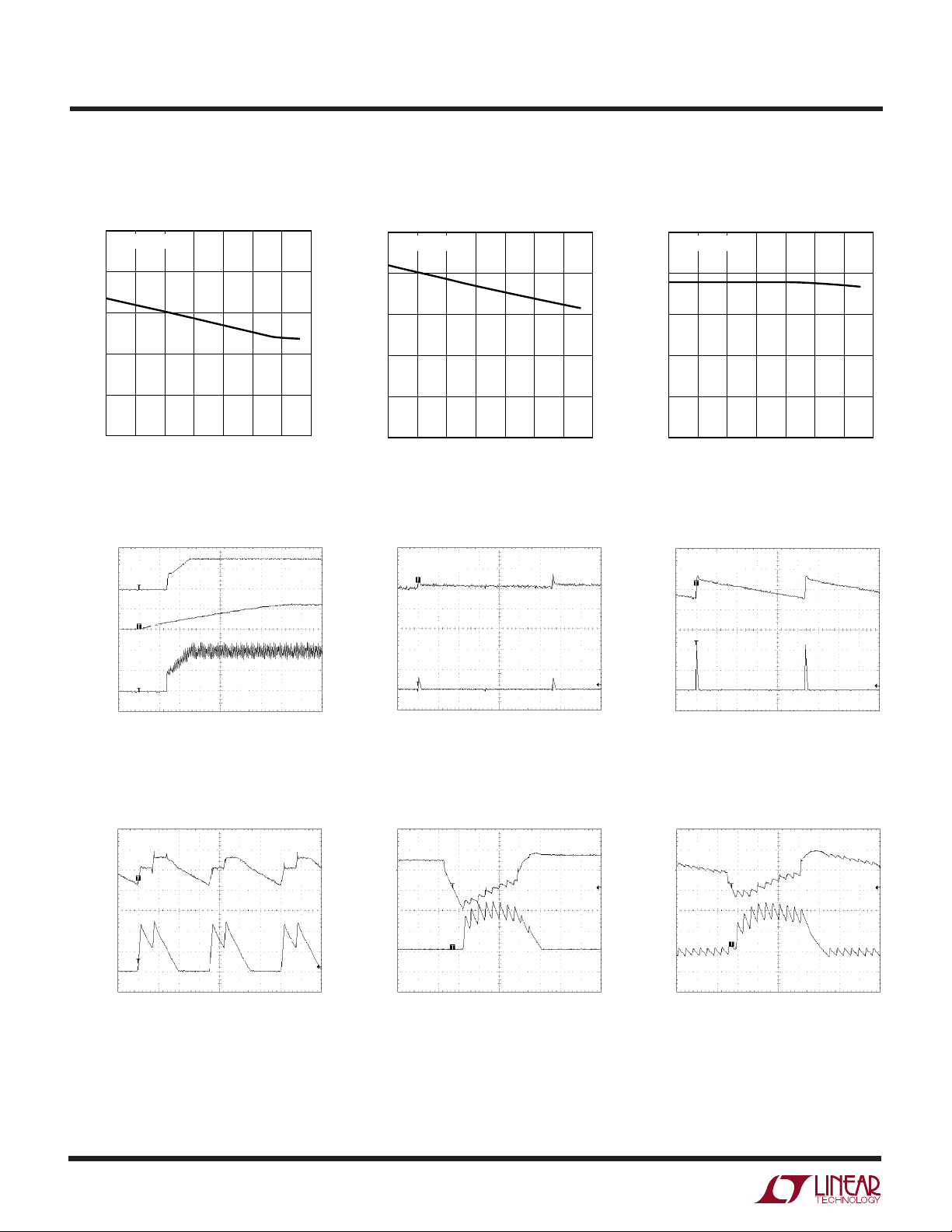
TYPICAL PERFOR A CE CHARACTERISTICS
Maximum Current Sense Threshold
vs Normalized Output Voltage
(Foldback)
80
70
60
50
40
30
20
10
MAXIMUM CURRENT SENSE THRESHOLD (mV)
0
0
25
NORMALIZED OUTPUT VOLTAGE (%)
50
75
100
1735 G10
Maximum Current Sense Threshold
vs V
RUN/SS
80
V
60
40
20
MAXIMUM CURRENT SENSE THRESHOLD (mV)
0
0
= 1.6V
SENSE(CM)
1234
V
(V)
RUN/SS
56
1735 G11
LTC1735
Maximum Current Sense Threshold
vs Sense Common Mode Voltage
80
76
72
68
64
MAXIMUM CURRENT SENSE THRESHOLD (mV)
60
1
0
COMMON MODE VOLTAGE (V)
3
2
4
5
1735 G12
Maximum Current Sense Threshold
vs ITH Voltage
90
80
70
60
50
40
30
20
10
0
–10
–20
MAXIMUM CURRENT SENSE THRESHOLD (mV)
–30
0.5
0
1.5
1
V
(V)
ITH
SENSE Pins Total Source Current
100
50
(µA)
0
SENSE
I
–50
–100
0
24
V
COMMON MODE VOLTAGE (V)
SENSE
Maximum Current Sense Threshold
V
vs Temperature
80
V
75
70
65
MAXIMUM CURRENT SENSE THRESHOLD (mV)
2
2.5
1735 G13
60
–40
= 1.6V
SENSE(CM)
–15 10 35 60
TEMPERATURE (°C)
85 110 135
1735 G18
(V)
ITH
V
ITH Voltage vs Load Current
1735 G16
2.5
VIN = 10V
= 3.3V
V
OUT
= 0.01Ω
R
SENSE
2.0
= 300kHz
f
O
CONTINUOUS
1.5
VOLTAGE (V)
1.0
TH
I
0.5
6
0
MODE
SYNCHRONIZED f = f
Burst Mode
OPERATION
0
234
1
LOAD CURRENT (A)
O
56
1735 G17
100
(%)
MAX
/I
OUT
AVERAGE OUTPUT CURRENT I
vs V
ITH
RUN/SS
2.5
V
= 0.7V
OSENSE
2.0
1.5
1.0
0.5
0
0
234
1
V
RUN/SS
(V)
Output Current vs Duty Cycle
I
(SYNC)
OUT/IMAX
80
60
40
20
f
= f
SYNC
0
O
0
20
DUTY CYCLE (%)
I
OUT/IMAX
(FREE RUN)
40 60 80
56
1735 G15
100
1735 G14
5
LTC1735
UW
TYPICAL PERFOR A CE CHARACTERISTICS
Oscillator Frequency
vs Temperature
300
C
= 47pF
OSC
290
280
270
FREQUENCY (kHz)
260
250
–40 –15
10
TEMPERATURE (°C)
Start-Up
V
OUT
1V/DIV
V
RUN/SS
5V/DIV
RUN/SS Pin Current
vs Temperature
0
V
= 0V
RUN/SS
–1
–2
–3
RUN/SS CURRENT (µA)
–4
60
35
85
110
135
1735 G19
–5
V
OUT
10mV/DIV
–40 –15
V
OUT(RIPPLE)
I
LOAD
60
35
10
TEMPERATURE (°C)
85
110
135
1735 G20
(Synchronized)
= 10mA I
FIGURE 1 FIGURE 1
FCB Pin Current vs Temperature
0
V
= 0.85V
FCB
–0.2
–0.4
–0.6
FCB CURRENT (µA)
–0.8
–1.0
–40 –15
V
OUT(RIPPLE)
35
10
TEMPERATURE (°C)
(Burst Mode Operation)
= 50mA
LOAD
V
OUT
20mV/DIV
60
85
110
135
1735 G21
5A/DIV
V
OUT
20mV/DIV
5A/DIV
I
L
= 15V 5ms/DIV
V
IN
V
= 1.6V
OUT
= 0.16Ω
R
LOAD
V
OUT(RIPPLE)
(Burst Mode Operation)
I
= 1.5A
LOAD
I
L
FCB = 5V 5µs/DIV
V
= 15V
IN
= 1.6V
V
OUT
I
L
I
L
5A/DIV
1735 G22 1735 G23 1735 G24
EXT SYNC f = f
V
= 15V
IN
= 1.6V
V
OUT
O
10µs/DIV
5A/DIV
FCB = 5V 50µs/DIV
= 15V
V
IN
V
= 1.6V
OUT
Load Step (Burst Mode Operation) Load Step (Continuous Mode)
FIGURE 1 FIGURE 1 FIGURE 1
V
OUT
V
OUT
50mV/DIV
I
L
5A/DIV
1735 G27 1735 G26 1735 G25
10mA TO 10µs/DIV
9A LOAD STEP
FCB = 5V
= 15V
V
IN
= 1.6V
V
OUT
50mV/DIV
5A/DIV
I
L
0A TO 10µs/DIV
9A LOAD STEP
FCB = 0V
= 15V
V
IN
= 1.6V
V
OUT
6

UUU
PI FU CTIO S
C
(Pin 1): External capacitor C
OSC
ground sets the operating frequency.
RUN/SS (Pin 2): Combination of Soft-Start and Run
Control Inputs. A capacitor to ground at this pin sets the
ramp time to full output current. The time is approximately
1.25s/µF. Forcing this pin below 1.5V causes the device to
be shutdown. In shutdown all functions are disabled.
Latchoff overcurrent protection is also invoked via this pin
as described in the Applications Information section.
ITH (Pin 3): Error Amplifier Compensation Point. The
current comparator threshold increases with this control
voltage. Nominal voltage range for this pin is 0V to 2.4V.
FCB (Pin 4): Forced Continuous/Synchronization Input.
Tie this pin to ground for continuous synchronous operation, to a resistive divider from the secondary output when
using a secondary winding or to INTVCC to enable Burst
Mode operation at low load currents. Clocking this pin with
a signal above 1.5V
allows cycle-skipping at low load currents and synchronizes the internal oscillator with the external clock.
SGND (Pin 5): Small-Signal Ground. All small-signal
components such as C
the loop compensation resistors and capacitor(s) should
single-point tie to this pin. This pin should, in turn, connect
to PGND.
V
OSENSE
external resistive divider across the output.
SENSE– (Pin 7): The (–) Input to the Current Comparator.
SENSE+ (Pin 8): The (+) Input to the Current Comparator.
Built-in offsets between SENSE– and SENSE+ pins in
conjunction with R
(Pin 6): Receives the feedback voltage from an
disables Burst Mode operation but
P–P
, CSS, the feedback divider plus
OSC
set the current trip threshold.
SENSE
from this pin to
OSC
LTC1735
EXTVCC (Pin 9): Input to the Internal Switch Connected to
INTVCC. This switch closes and supplies VCC power whenever EXTVCC is higher than 4.7V. See EXTVCC connection
in the Applications Information section. Do not exceed 7V
on this pin and ensure EXTVCC ≤ VIN.
PGND (Pin 10): Driver Power Ground. Connects to the
source of bottom N-channel MOSFET, the anode of the
Schottky diode, and the (–) terminal of CIN.
BG (Pin 11): High Current Gate Drive for Bottom
N-Channel MOSFET. Voltage swing at this pin is from
ground to INTVCC.
INTVCC (Pin 12): Output of the Internal 5.2V Regulator and
EXTVCC Switch. The driver and control circuits are powered from this voltage. Decouple to power ground with a
1µF ceramic capacitor placed directly adjacent to the IC
together with a minimum of 4.7µF tantalum or other low
ESR capacitor.
VIN (Pin 13): Main Supply Pin. Must be closely decoupled
to power ground.
SW (Pin 14): Switch Node Connection to Inductor and
Bootstrap Capacitor. Voltage swing at this pin is from a
Schottky diode (external) voltage drop below ground to
VIN.
BOOST (Pin 15): Supply to Topside Floating Driver. The
bootstrap capacitor is returned to this pin. Voltage swing
at this pin is from a diode drop below INTVCC to (VIN +
INTVCC).
TG (Pin 16): High Current Gate Drive for Top N-Channel
MOSFET. This is the output of a floating driver with a
voltage swing equal to INTVCC superimposed on the
switch node voltage SW.
7
LTC1735
UU
W
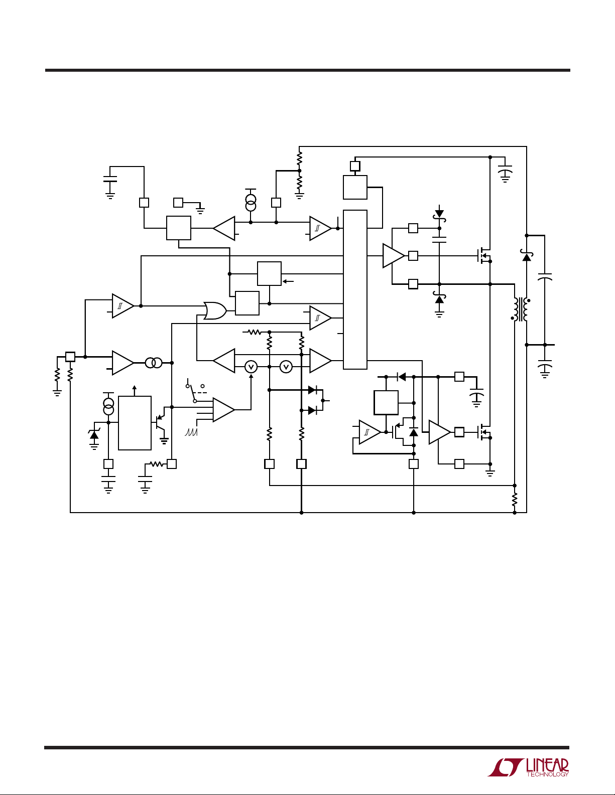
FU CTIO AL DIAGRA
C
OSC
1 5 4
OSC
SYNC
OSC
OV
+
–
0.86V
V
OSENSE
V
FB
6
0.8V
R2
R1
1.2µA
6V
RUN/SS
C
SS
2
gm =1.3m
–
EA
+
CURRENT
LATCHOFF
SD
RUN
SOFT-
START
+
OVER-
C
C
Ω
R
C
0.86V
4(V
)
FB
SLOPE COMP
I
TH
ICMP
BURST
DISABLE
FC
0.17µA
C
–
+
1.2V 0.8V
FORCE BOT
S
R
2.4V
–
I
1
+
A
BUFFERED
I
TH
SENSE
Q
2k
+– –+
+
FCBSGNDC
DROP
OUT
DET
TOP ON
45k
3mV
30k 30k
0.55V
BOT
–
+
+
–
45k
–
+
SENSE
V
IN
V
13
IN
UVL
0.8V
REF
FC
F
TOP
SWITCH
LOGIC
B
SD
IREV
I
2
INTV
4.7V
–
BOT
V
IN
CC
5.2V
LDO
REG
+
–
EXTV
CC
BOOST
15
TG
16
SW
14
9783
INTV
CC
D
B
C
B
D
1
INTV
C
INTVCC
PGND
CC
12
BG
11
10
+
C
IN
V
SEC
+
C
SEC
V
OUT
+
C
OUT
+
8
R
SENSE
1735 FD

OPERATIO
LTC1735
U
(Refer to Functional Diagram)
Main Control Loop
The LTC1735 uses a constant frequency, current mode
step-down architecture. During normal operation, the top
MOSFET is turned on each cycle when the oscillator sets
the RS latch and turned off when the main current comparator I1 resets the RS latch. The peak inductor current at
which I1 resets the RS latch is controlled by the voltage on
Pin 3 (ITH), which is the output of error amplifier EA. Pin␣ 6
(V
OSENSE
receive an output feedback voltage VFB from an external
resistive divider. When the load current increases, it
causes a slight decrease in VFB relative to the 0.8V reference, which in turn causes the ITH voltage to increase until
the average inductor current matches the new load current. While the top MOSFET is off, the bottom MOSFET is
turned on until either the inductor current starts to reverse,
as indicated by current comparator I2, or the beginning of
the next cycle.
The top MOSFET driver is powered from a floating bootstrap capacitor CB. This capacitor is normally recharged
from INTVCC through an external diode when the top
MOSFET is turned off. As VIN decreases towards V
converter will attempt to turn on the top MOSFET continuously (“dropout’’). A dropout counter detects this condition and forces the top MOSFET to turn off for about 500ns
every tenth cycle to recharge the bootstrap capacitor.
), described in the pin functions, allows EA to
, the
OUT
conditions that may overvoltage the output. In this case,
the top MOSFET is turned off and the bottom MOSFET is
turned on until the overvoltage condition is cleared.
Foldback current limiting for an output shorted to ground
is provided by amplifier A. As V
the buffered ITH input to the current comparator is gradually pulled down to a 0.86V clamp. This reduces peak
inductor current to about 1/4 of its maximum value.
Low Current Operation
The LTC1735 has three low current modes controlled by
the FCB pin. Burst Mode operation is selected when the
FCB pin is above 0.8V (typically tied to INTVCC). In Burst
Mode operation, if the error amplifier drives the ITH voltage
below 0.86V, the buffered ITH input to the current comparator will be clamped at 0.86V. The inductor current
peak is then held at approximately 20mV/R
1/4 of maximum output current). If ITH then drops below
0.5V, the Burst Mode comparator B will turn off both
MOSFETs to maximize efficiency. The load current will be
supplied solely by the output capacitor until ITH rises
above the 60mV hysteresis of the comparator and switching is resumed. Burst Mode operation is disabled by
comparator F when the FCB pin is brought below 0.8V.
This forces continuous operation and can assist secondary winding regulation.
OSENSE
drops below 0.6V,
(about
SENSE
The main control loop is shut down by pulling Pin 2
(RUN/SS) low. Releasing RUN/SS allows an internal 1.2µA
current source to charge soft-start capacitor CSS. When
CSS reaches 1.5V, the main control loop is enabled with the
ITH voltage clamped at approximately 30% of its maximum
value. As CSS continues to charge, ITH is gradually released allowing normal operation to resume. If V
not reached 70% of its final value when CSS has charged
to 4.1V, latchoff can be invoked as described in the
Applications Information section.
The internal oscillator can be synchronized to an external
clock applied to the FCB pin and can lock to a frequency
between 90% and 130% of its nominal rate set by capacitor C
An overvoltage comparator, OV, guards against transient
overshoots (>7.5%) as well as other more serious
OSC
.
OUT
has
When the FCB pin is driven by an external oscillator, a low
noise cycle-skipping mode is invoked and the internal
oscillator is synchronized to the external clock by comparator C. In this mode the 25% minimum inductor
current clamp is removed, providing constant frequency
discontinuous operation over the widest possible output
current range. This constant frequency operation is not
quite as efficient as Burst Mode operation, but provides a
lower noise, constant frequency spectrum.
The FCB pin is tied to ground when forced continuous
operation is desired. This is the least efficient mode, but is
desirable in certain applications. The output can source or
sink current in this mode. When sinking current while in
forced continuous operation, current will be forced back
into the main power supply potentially boosting the input
supply to dangerous voltage levels—BEWARE.
9

LTC1735
OPERATIO
U
(Refer to Functional Diagram)
Foldback Current, Short-Circuit Detection and
Short-Circuit Latchoff
The RUN/SS capacitor, CSS, is used initially to limit the
inrush current of the switching regulator. After the controller has been started and been given adequate time to
charge up the output capacitors and provide full load current, CSS is used as a short-circuit time-out circuit. If the
output voltage falls to less than 70% of its nominal output
voltage, CSS begins discharging on the assumption that
the output is in an overcurrent and/or short-circuit condition. If the condition lasts for a long enough period as
determined by the size of CSS, the controller will be shut
down until the RUN/SS pin voltage is recycled. This builtin latchoff can be overridden by providing a current >5µA
at a compliance of 5V to the RUN/SS pin. This current
shortens the soft-start period but also prevents net discharge of C
condition. Foldback current limiting is activated when the
during an overcurrent and/or short-circuit
SS
U
WUU
APPLICATIO S I FOR ATIO
output voltage falls below 70% of its nominal level whether
or not the short-circuit latchoff circuit is enabled.
INTVCC/EXTVCC POWER
Power for the top and bottom MOSFET drivers and most
of the internal circuitry of the LTC1735 is derived from the
INTVCC pin. When the EXTVCC pin is left open, an internal
5.2V low dropout regulator supplies the INTVCC power
from VIN. If EXTVCC is raised above 4.7V, the internal
regulator is turned off and an internal switch connects
EXTVCC to INTVCC. This allows a high efficiency source,
such as the primary or a secondary output of the converter
itself, to provide the INTVCC power. Voltages up to 7V can
be applied to EXTVCC for additional gate drive capability.
To provide clean start-up and to protect the MOSFETs,
undervoltage lockout is used to keep both MOSFETs off
until the input voltage is above 3.5V.
The basic LTC1735 application circuit is shown in Figure␣ 1
on the first page. External component selection is driven
by the load requirement and begins with the selection of
R
Next, the power MOSFETs and D1 are selected. The
operating frequency and the inductor are chosen based
largely on the desired amount of ripple current. Finally, C
is selected for its ability to handle the large RMS current
into the converter and C
ESR to meet the output voltage ripple and transient specifications. The circuit shown in Figure 1 can be configured
for operation up to an input voltage of 28V (limited by the
external MOSFETs).
R
R
The LTC1735 current comparator has a maximum threshold of 75mV/R
SGND to 1.1(INTVCC). The current comparator threshold
sets the peak of the inductor current, yielding a maximum
average output current I
half the peak-to-peak ripple current, ∆IL.
. Once R
SENSE
Selection for Output Current
SENSE
is chosen based on the required output current.
SENSE
is known, C
SENSE
is chosen with low enough
OUT
and an input common mode range of
SENSE
equal to the peak value less
MAX
and L can be chosen.
OSC
IN
Allowing a margin for variations in the LTC1735 and
external component values yields:
mV
R
SENSE
C
Selection for Operating Frequency and
OSC
Synchronization
The choice of operating frequency and inductor value is a
trade-off between efficiency and component size. Low
frequency operation improves efficiency by reducing
MOSFET switching losses, both gate charge loss and
transition loss. However, lower frequency operation requires more inductance for a given amount of ripple
current.
The LTC1735 uses a constant frequency architecture with
the frequency determined by an external oscillator capacitor C
OSC
voltage on C
C
is charged by a fixed current. When the voltage on the
OSC
50
=
I
MAX
. Each time the topside MOSFET turns on, the
is reset to ground. During the on-time,
OSC
10
 Loading...