

Linear Technology LTC1731ES8-4.2, LTC1731-4.2, LTC1731EMS8-4.2 Datasheet
FEATURES
Final Electrical Specifications
LTC1731-4.2
Lithium-Ion Linear
Battery Charger Controller
December 1999
U
DESCRIPTION
■
Complete Linear Charger Controller for
1-Cell Lithium-Ion Batteries
■
1% Voltage Accuracy
■
Programmable Charge Current
■
C/10 Charge Current Detection Output
■
Programmable Charge Termination Timer
■
Space Saving 8-Pin MSOP Package
■
Automatic Sleep Mode When Input Supply
is Removed (Only 7µA Battery Drain)
■
Automatic Trickle Charging of Low Voltage Cells
■
Programmable for Constant-Current-Only Mode
U
APPLICATIONS
■
Cellular Phones
■
Handheld Computers
■
Charging Docks and Cradles
■
Programmable Current Source
The LTC®1731-4.2 is a complete constant-current/constant-voltage linear charge controller for lithium-ion batteries. Nickel-cadmium (NiCd) and nickel-metal-hydride
(NiMH) batteries can also be charged with constant
current using external termination. The external sense
resistor sets the charge current with 5% accuracy. An
internal resistor divider and precision reference set the
final float potential with 1% accuracy. The output float
voltage is set internally to 4.2V.
When the input supply is removed, the LTC1731-4.2
automatically enters a low current sleep mode, dropping
the battery drain current to 5µA. An internal comparator
detects the end-of-charge (C/10) condition while a programmable timer, using an external capacitor, sets the
total charge time. Fully discharged cells are automatically
trickle charged at 10% of the programmed current until
cell voltage exceeds 2.5V.
The LTC1731-4.2 is available in the 8-pin MSOP and SO
packages.
, LTC and LT are registered trademarks of Linear Technology Corporation.
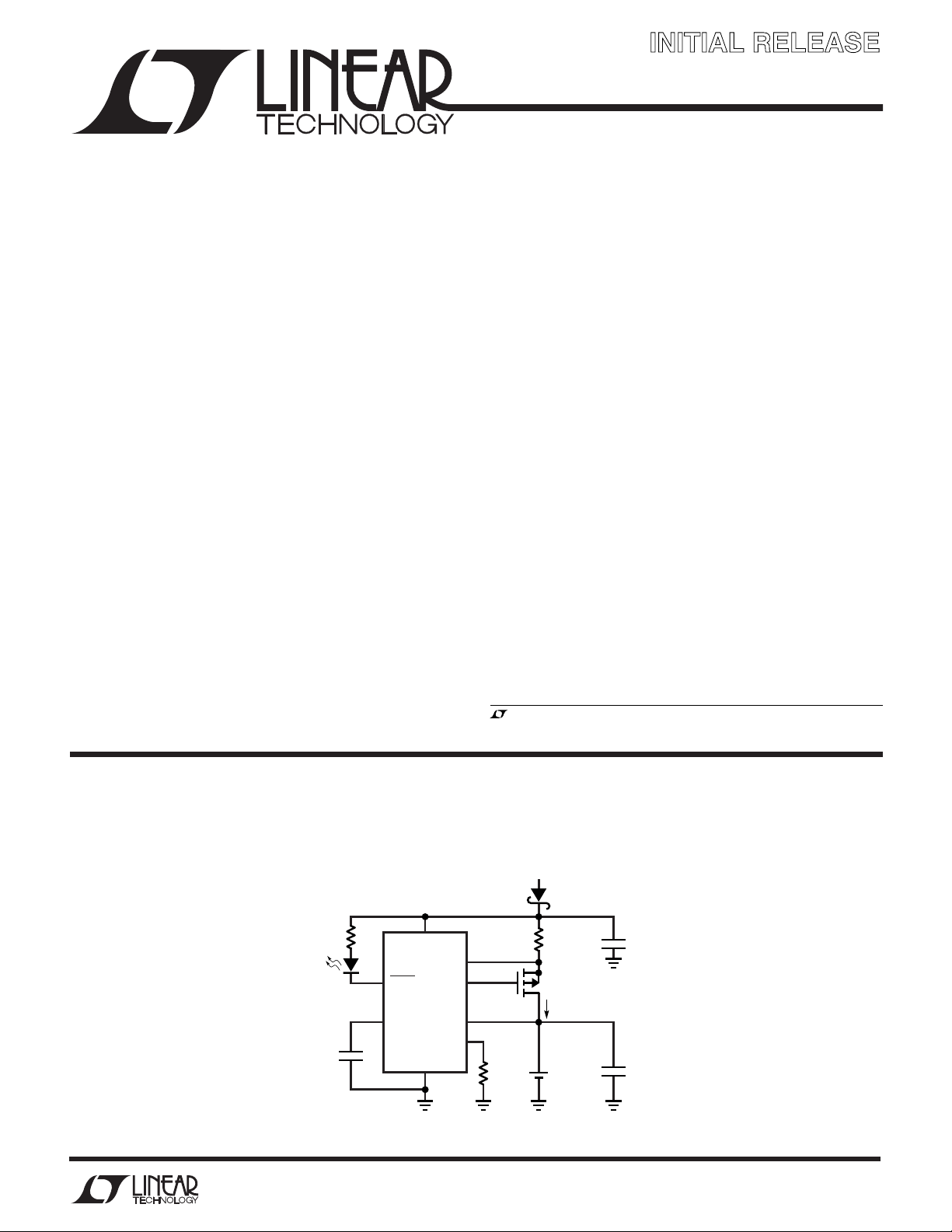
TYPICAL APPLICATION
U
500mA Li-Ion Charger
V
IN
5V TO 15V
MBRM120T3
1k
2
3
C
TIMER
0.1µF
*SHUTDOWN INVOKED BY FLOATING THE PROG PIN
Information furnished by Linear Technology Corporation is believed to be accurate and reliable.
However, no responsibility is assumed for its use. Linear Technology Corporation makes no representation that the interconnection of its circuits as described herein will not infringe on existing patent rights.
V
CC
CHRG
LTC1731-4.2
TIMER
GND
7
SENSE
DRV
BAT
PROG
4
8
6
1
5
R
PROG
19.6k
*
R
SENSE
0.2Ω
Q1
Si9430DY
I
BAT
+
Li-ION
CELL
1µF
= 500mA
10µF
1731 TA01
1
LTC1731-4.2
WW
W
ABSOLUTE MAXIMUM RATINGS
U
(Note 1)
Input Supply Voltage (VCC) ................................... 13.2V
Input Voltage (SENSE, DRV, BAT,
TIMER, PROG) ....................... –0.3V to (VCC + 0.3V)
Output Voltage (CHRG) ......................... –0.3V to 13.2V
U
W
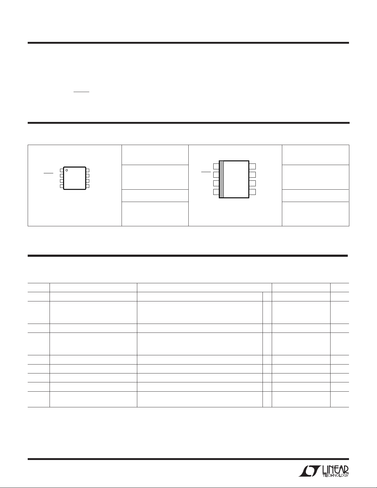
PACKAGE/ORDER INFORMATION
ORDER PART
TOP VIEW
BAT
1
CHRG
2
TIMER
3
GND
4
MS8 PACKAGE
8-LEAD PLASTIC MSOP
T
= 150°C, θJA = 180°C/W
JMAX
8
7
6
5
SENSE
V
CC
DRV
PROG
NUMBER
LTC1731EMS8-4.2
MS8 PART MARKING
LTKQ
Operating Temperature Range (Note 2) .....–40° to 85°C
Storage Temperature Range ................. –65°C to 150°C
Lead Temperature (Soldering, 10 sec)..................300°C
U
ORDER PART
NUMBER
LTC1731ES8-4.2
S8 PART MARKING
173142
BAT
CHRG
TIMER
GND
T
JMAX
TOP VIEW
1
2
3
4
S8 PACKAGE
8-LEAD PLASTIC SO
= 150°C, θJA = 125°C/W
8
SENSE
V
7
CC
DRV
6
PROG
5
Consult factory for Industrial and Military grade parts.
ELECTRICAL CHARACTERISTICS
The ● denotes the specifications which apply over the full operating
temperature range, otherwise specifications are at TA = 25°C. VCC = 6V unless otherwise noted.
SYMBOL PARAMETER CONDITIONS MIN TYP MAX UNITS
V
CC
I
CC
V
BAT
I
BAT
I
TRIKL
V
TRIKL
V
UV
∆V
V
MSD
UV
Input Supply Voltage ● 4.5 12 V
Input Supply Current Charger On, Current Mode ● 13 mA
Shutdown Mode
Sleep Mode (Battery Drain Current) 7 20 µA
Regulated Output Voltage LTC1731-4.2 (5V ≤ VCC ≤ 12V) ● 4.158 4.2 4.242 V
Current Mode Charge Current R
Trickle Charge Current V
Trickle Charge Threshold Voltage From Low to High ● 2.4 2.457 2.55 V
VCC Undervoltage Lockout Voltage From Low to High ● 4.1 4.5 V
VCC Undervoltage Lockout Hysteresis 200 mV
Manual Shutdown Threshold Voltage PROG Pin Low to High 2.457 V
= 19.6k, R
PROG
R
= 19.6k, R
PROG
= 97.6k, R
R
PROG
= 2V, R
BAT
PROG Pin High to Low 2.446 V
PROG
= 0.2Ω 465 500 535 mA
SENSE
= 0.2Ω ● 415 585 mA
SENSE
= 0.2Ω 70 100 130 mA
SENSE
= 19.6k, I
TRIKL
= (VCC – V
)/0.2Ω ● 30 50 95 mA
SENSE
● 12 mA
2
LTC1731-4.2
ELECTRICAL CHARACTERISTICS
temperature range, otherwise specifications are at TA = 25°C. VCC = 6V unless otherwise noted.
SYMBOL PARAMETER CONDITIONS MIN TYP MAX UNITS
V
ASD
V
DIS
I
PROG
V
PROG
I
CHRG
V
CHRG
I
C/10
t
TIMER
V
CLAMP
Note 1: Absolute Maximum Ratings are those values beyond which the life
of a device may be impaired.
Automatic Shutdown Threshold Voltage (VCC – V
(V
Voltage Mode Disable Threshold Voltage V
PROG Pin Current Internal Pull-Up Current, No R
PROG Pin Load Regulation PROG Pin Source Current, ∆V
PROG Pin Voltage R
CHRG Pin Weak Pull-Down Current V
CHRG Pin Output Low Voltage I
End of Charge Indication Current Level R
TIMER Accuracy C
DRV Pin Clamp Voltage V
TIMER
PROG
CHRG
CHRG
PROG
TIMER
CLAMP
The ● denotes the specifications which apply over the full operating
) High to Low 30 54 90 mV
BAT
– V
CC
) Low to High 40 69 100 mV
BAT
● 5.6 V
PROG
≤ 5mV ● 300 µA
PROG
=19.6k 2.457 V
= 1V 70 100 130 µA
= 5mA 0.6 1.2 V
= 19.6k, R
= 0.1µF10%
= VCC – V
= 0.2Ω ● 25 50 100 mA
SENSE
, I
DRV
= 50µA 6.5 V
DRIVE
Note 2: The LTC1731-4.2 is guaranteed to meet performance
specifications from 0°C to 70°C. Specifications over the –40°C to 85°C
operating temperature range are assured by design, characterization and
correlation with statistical process controls. Guaranteed I grade parts are
available, consult factory.
2.5 µA
UUU
PIN FUNCTIONS
BAT (Pin 1): Battery Sense Input. A bypass capacitor of at
least 10µF is required to keep the loop stable when the
battery is not connected. A precision internal resistor
divider sets the final float potential on this pin. The resistor
divider is disconnected in sleep mode.
CHRG (Pin 2): Open-Drain Charge Status Output. When
the battery is being charged, the CHRG pin is pulled low by
an internal N-channel MOSFET. When the charge current
drops to 10% of the full-scale current for at least 0.32
seconds, the N-channel MOSFET turns off and a 100µA
current source is connected from the CHRG pin to GND.
When the timer runs out or the input supply is removed,
the current source will be disconnected and the CHRG pin
is forced into a high impedance state.
TIMER (Pin 3): Timer Capacitor and Constant-Voltage
Mode Disable Input Pin. The timer period is set by placing
a capacitor, C
(C
• 3 hours)/(0.1µF). When the TIMER pin is
TIMER
, to GND. The timer period is t
TIMER
TIMER
=
connected to VCC, the constant-voltage mode is disabled
and the chip will operate in constant-current mode only.
Short the TIMER pin to GND to disable the internal timer
function.
GND (Pin 4): Ground.
PROG (Pin 5): Charge Current Program and Shutdown
Input Pin. The charge current is programmed by connecting a resistor, R
= (V
• 800Ω)/(R
PROG
to ground. The charge current is I
PROG
PROG
• R
). The IC can be forced
SENSE
BAT
into shutdown by floating the PROG pin and allowing the
internal 2.5µA current source to pull the pin above the
2.457V shutdown threshold voltage.
DRV (Pin 6): Drive Output Pin for the P-Channel MOSFET
or PNP Transistor. The impedance is high at this pin,
therefore, a high gain PNP pass transistor should be used.
The DRV pin is internally clamped to 8V (max) below VCC.
VCC (Pin 7): Positive Input Supply Voltage. When V
BAT
is
within 54mV of VCC, the LTC1731-4.2 is forced into sleep
mode, dropping ICC to 7µA. VCC ranges from 4.5V to 12V.
Bypass this pin with a 1µF capacitor.
SENSE (Pin 8): Current Sense Input. A sense resistor,
R
, must be connected from VCC to the SENSE pin.
SENSE
This resistor is chosen using the following equation:
R
SENSE
= (V
• 800Ω)/(R
PROG
PROG
• I
BAT
)
3
 Loading...