

Linear Technology LTC1709 Datasheet
LTC1709
2-Phase, 5-Bit Adjustable,
High Efficiency, Synchronous Step-Down
FEATURES
■
Two Ouput Stages Operate Antiphase Reducing
Input Capacitance and Power Supply Noise
■
5-Bit VID Control (VRM 8.4 Compliant)
V
: 1.3V to 3.5V in 50mV/100mV Steps
OUT
■
Current Mode Control Ensures Current Sharing
■
True Remote Sensing Differential Amplifier
■
OPTI-LOOPTM Compensation Minimizes C
■
Programmable Fixed Frequency: 150kHz to
OUT
300kHz—Effective 300kHz to 600kHz Switching
Frequency
■
±
1% Output Voltage Accuracy
■
Wide VIN Range: 4V to 36V Operation
■
Adjustable Soft-Start Current Ramping
■
Internal Current Foldback
■
Short-Circuit Shutdown Timer with Defeat Option
■
Overvoltage Soft-Latch Eliminates Nuisance Trips
■
Low Shutdown Current: 20µA
■
Small 36-Lead Narrow (0.209") SSOP Package
U
APPLICATIO S
■
Desktop Computers
■
Internet/Network Servers
■
Large Memory Arrays
■
DC Power Distribution Systems
■
Battery Chargers
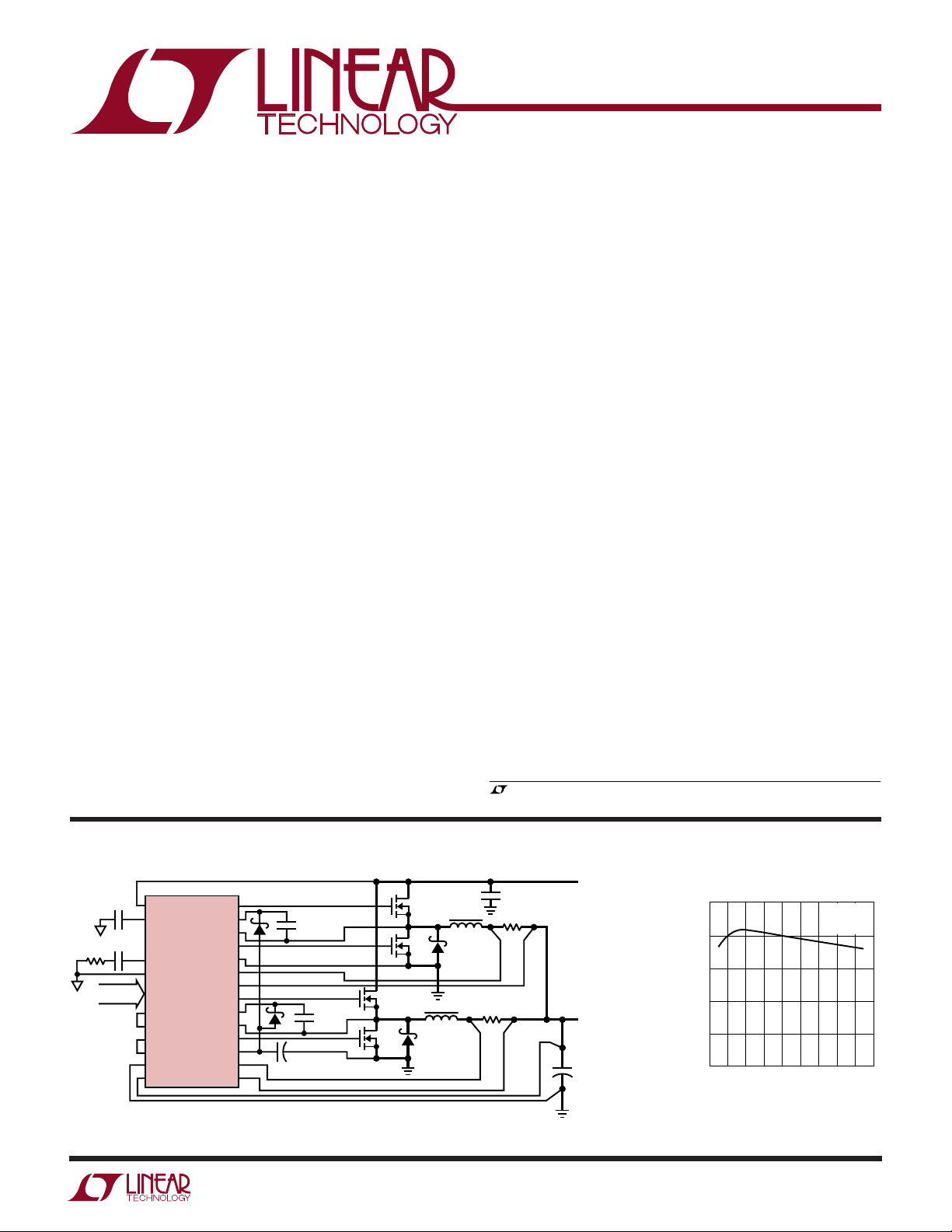
Switching Regulator
U
DESCRIPTIO
The LTC®1709 is a 2-phase, VID programmable, synchronous step-down switching regulator controller that drives
all N-channel external power MOSFET stages in a fixed
frequency architecture. The 2-phase controller drives its
two output stages out of phase at frequencies up to
300kHz to minimize the RMS ripple currents in both input
and output capacitors. The 2-phase technique effectively
multiplies the fundamental frequency by two, improving
transient response while operating each channel at a
optimum frequency for efficiency. Thermal design is also
simplified.
An internal differential amplifier provides true remote
sensing of the regulated supply’s positive and negative
output terminals as required in high current applications.
The RUN/SS pin provides soft-start and optional timed,
short-circuit shutdown. Current foldback limits MOSFET
dissipaton during short-circuit conditions when overcurrent
latchoff is disabled. OPTI-LOOP compensation allows the
transient response to be optimized for a wide range of
output capacitors and ESR values.
, LTC and LT are registered trademarks of Linear Technology Corporation.
OPTI-LOOP is a trademark of Linear Technology Corporation.
TYPICAL APPLICATIO
S
0.1µF
V
IN
RUN/SS
1.2nF
15k
5 VID BITS
I
TH
SGND
VID0–VID4
EAIN
FBOUT
SENSEIN
V
DIFFOUT
–
V
OS
+
V
OS
Q1–Q4 2× FAIRCHILD FDS7760A OR SILICONIX Si4874
TG1
SW1
BG1
PGND
TG2
SW2
BG2
S
S
+
–
S
S
S
CC
+
–
10µF
+
LTC1709
BOOST 1
SENSE1
SENSE1
BOOST2
INTV
SENSE 2
SENSE 2
Figure 1. High Current 2-Phase Step-Down Converter
0.47µF
S
U
0.47µF
V
IN
+
5V TO 28V
V
OUT
1.3V TO 3.5V
40A
C
OUT
1000µF
4V
×2
1709 TA01
100
90
80
70
EFFICIENCY (%)
60
50
10µF ×4
Q1
Q2
Q3
Q4
35V
0.002Ω
1µH
0.002Ω
1µH
Efficiency Curve
515
10
0
LOAD CURRENTS (A)
VIN = 5V
V
f
25 45
30
20
= 1.6V
OUT
= 200kHz
S
35
40
1709 TA01a
1
LTC1709
WW
W
U
ABSOLUTE AXI U RATI GS
(Note 1)
Input Supply Voltage (VIN).........................36V to –0.3V
Topside Driver Voltages (BOOST 1, 2).......42V to –0.3V
Switch Voltage (SW1, 2) .............................36V to –5 V
SENSE 1+, SENSE 2+, SENSE 1–,
SENSE 2– Voltages....................... (1.1)INTVCC to –0.3V
EAIN, V
AMPMD, V
VID0–VID4, Voltages ...................................7V to –0.3V
Boosted Driver Voltage (BOOST-SW) ..........7V to –0.3V
PLLFLTR, PLLIN, V
ITH Voltage................................................2.7V to –0.3V
Peak Output Current <1µs(TGL1, 2; BG1, 2).............. 3A
INTVCC RMS Output Current................................ 50mA
Operating Ambient Temperature Range
(Note 2) .................................................. – 40°C to 85°C
Junction Temperature (Note 3)............................. 125°C
Storage Temperature Range ................. –65°C to 150°C
Lead Temperature (Soldering, 10 sec)..................300°C
OS
+
–
, V
, EXTVCC, INTVCC, RUN/SS,
OS
, ATTENIN, ATTENOUT,
BIAS
DIFFOUT
Voltages .... INTVCC to –0.3V
UUW
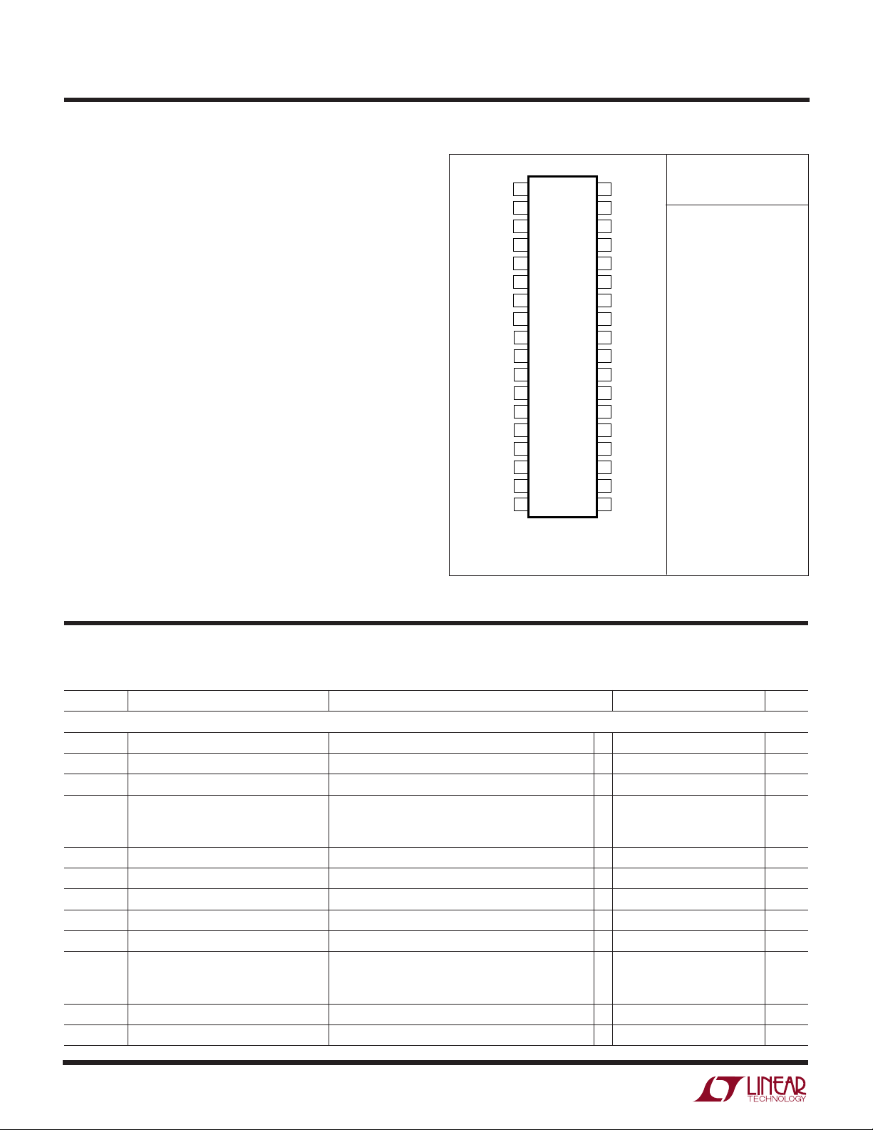
PACKAGE/ORDER I FOR ATIO
RUNN/SS
SENSE 1
SENSE 1
EAIN
PLLFLTR
PLLIN
SGND
V
DIFFOUT
VOS–
V
OS
SENSE 2
SENSE 2
ATTENOUT
ATTENIN
VID0
VID1
TOP VIEW
1
+
2
–
3
4
5
6
7
NC
8
I
TH
9
10
11
12
+
–
13
+
14
15
16
17
18
G PACKAGE
36-LEAD PLASTIC SSOP
T
= 125°C, θJA = 85°C/W
JMAX
36
35
34
33
32
31
30
29
28
27
26
25
24
23
22
21
20
19
NC
TG1
SW1
BOOST 1
V
IN
BG1
EXTV
CC
INTV
CC
PGND
BG2
BOOST 2
SW2
TG2
AMPMD
V
BIAS
VID4
VID3
VID2
ORDER PART
NUMBER
LTC1709EG
Consult factory for Industrial and Military grade parts.
ELECTRICAL CHARACTERISTICS
temperature range, otherwise specifications are at T
The ● denotes the specifications which apply over the full operating
= 25°C. V
A
= 15V, V
IN
= 5V unless otherwise noted.
RUN/SS
SYMBOL PARAMETER CONDITIONS MIN TYP MAX UNITS
Main Control Loop
V
EAIN
V
SENSEMAX
I
INEAIN
V
LOADREG
V
REFLNREG
V
OVL
Regulated Feedback Voltage (Note 4); ITH Voltage = 1.2V ● 0.792 0.800 0.808 V
Maximum Current Sense Threshold V
–
= 5V ● 62 75 88 mV
SENSE
Feedback Current (Note 4) –5 –50 nA
Output Voltage Load Regulation (Note 4)
Measured in Servo Loop; ∆I
Measured in Servo Loop; ∆I
Voltage: 1.2V to 0.7V ● 0.1 0.5 %
TH
Voltage: 1.2V to 2V ● –0.1 –0.5 %
TH
Reference Voltage Line Regulation VIN = 3.6V to 30V (Note 4) 0.002 0.02 %/V
Output Overvoltage Threshold Measured at V
EAIN
● 0.84 0.86 0.88 V
UVLO Undervoltage Lockout VIN Ramping Down 3 3.5 4 V
g
m
g
mOL
I
Q
I
RUN/SS
V
RUN/SS
Transconductance Amplifier g
m
ITH = 1.2V; Sink/Source 5µA; (Note 4) 3 mmho
Transconductance Amplifier Gain ITH = 1.2V; (gmxZL; No Ext Load); (Note 4) 1.5 V/mV
Input DC Supply Current (Note 5)
Normal Mode EXTV
Shutdown V
Soft-Start Charge Current V
RUN/SS Pin ON Arming V
Tied to V
CC
= 0V 20 40 µA
RUN/SS
= 1.9V –0.5 –1.2 µA
RUN/SS
Rising 1.0 1.5 1.9 V
RUN/SS
OUT
; V
= 5V 470 µA
OUT
2
LTC1709
ELECTRICAL CHARACTERISTICS
temperature range, otherwise specifications are at T
The ● denotes the specifications which apply over the full operating
= 25°C. V
A
= 15V, V
IN
= 5V unless otherwise noted.
RUN/SS
SYMBOL PARAMETER CONDITIONS MIN TYP MAX UNITS
V
RUN/SSLO
I
SCL
I
SDLHO
I
SENSE
DF
MAX
RUN/SS Pin Latchoff Arming V
RUN/SS Discharge Current Soft Short Condition V
Shutdown Latch Disable Current V
Total Sense Pins Source Current Each Channel: V
Rising from 3V 4.1 4.5 V
RUN/SS
= 0.5V; 0.5 2 4 µA
= 4.5V
V
RUN/SS
= 0.5V 1.6 5 µA
EAIN
EAIN
SENSE1–, 2
– = V
SENSE1+, 2
+ = 0V –85 –60 µA
Maximum Duty Factor In Dropout 98 99.5 %
Top Gate Transition Time: (Note 6)
TG1, 2 t
TG1, 2 t
Rise Time C
r
Fall Time C
f
= 3300pF 30 90 ns
LOAD
= 3300pF 40 90 ns
LOAD
Bottom Gate Transition Time: (Note 6)
BG1, 2 t
BG1, 2 t
TG/BG t
BG/TG t
t
ON(MIN)
Rise Time C
r
Fall Time C
f
Top Gate Off to Bottom Gate On Delay (Note 6)
1D
Synchronous Switch-On Delay Time C
Bottom Gate Off to Top Gate On Delay (Note 6)
2D
Top Switch-On Delay Time C
Minimum On-Time Tested with a Square Wave (Note 7) 180 200 ns
= 3300pF 30 90 ns
LOAD
= 3300pF 20 90 ns
LOAD
= 3300pF Each Driver 90 ns
LOAD
= 3300pF Each Driver 90 ns
LOAD
Internal VCC Regulator
V
INTVCC
V
LDO
V
LDO
V
EXTVCC
V
LDOHYS
Internal VCC Voltage 6V < VIN < 30V; V
INT INTVCC Load Regulation ICC = 0 to 20mA; V
EXT EXTVCC Voltage Drop ICC = 20mA; V
EXTVCC
EXTVCC Switchover Voltage ICC = 20mA, EXTV
EXTVCC Switchover Hysteresis ICC = 20mA, EXTV
= 4V 4.8 5.0 5.2 V
EXTVCC
= 4V 0.2 1.0 %
EXTVCC
= 5V 120 240 mV
Ramping Positive ● 4.5 4.7 V
CC
Ramping Negative 0.2 V
CC
VID Parameters
R
ATTEN
Resistance Between ATTENIN and 20 kΩ
ATTENOUT Pins
ATTEN
R
PULLUP
VID
THLOW
VID
THHIGH
VID
LEAK
Resistive Divider Worst-Case Error Programmed from 1.3V to 2.05V (VID4 = 0) ● –0.25 +0.25 %
ERR
Programmed from 2.1V to 3.5V (VID4 = 1)
● –0.35 +0.25 %
VID0–VID4 Pull-Up Resistance (Note 8) 40 kΩ
VID0–VID4 Logic Threshold Low 0.4 V
VID0–VID4 Logic Threshold High 1.6 V
VID0–VID4 Leakage V
< VID0–VID4 < 7V 1 µA
BIAS
Oscillator and Phase-Locked Loop
f
NOM
f
LOW
f
HIGH
R
PLLIN
I
PLLFLTR
R
RELPHS
Nominal Frequency V
Lowest Frequency V
Highest Frequency V
= 1.2V 190 220 250 kHz
PLLFLTR
= 0V 120 140 160 kHz
PLLFLTR
≥ 2.4V 280 310 360 kHz
PLLFLTR
PLLIN Input Resistance 50 kΩ
Phase Detector Output Current
Sinking Capability f
Sourcing Capability f
PLLIN
PLLIN
< f
> f
OSC
OSC
–15 µA
15 µA
Controller 2-Controller 1 Phase 180 Deg
Differential Amplifier/Op Amp Gain Block (Note 9)
A
DA
CMRR
Gain Differential Amp Mode 0.995 1 1.005 V/V
Common Mode Rejection Ratio Differential Amp Mode; 0V < VCM < 5V 46 55 dB
DA
3
LTC1709
ELECTRICAL CHARACTERISTICS
temperature range, otherwise specifications are at T
The ● denotes the specifications which apply over the full operating
= 25°C. V
A
= 15V, V
IN
= 5V unless otherwise noted.
RUN/SS
SYMBOL PARAMETER CONDITIONS MIN TYP MAX UNITS
R
IN
V
OS
I
B
A
OL
V
CM
CMRR
PSRR
I
CL
V
O(MAX)
GBW Gain-Bandwidth Product Op Amp Mode; I
Input Resistance Differential Amp Mode; Measured at VOS+ Input 80 kΩ
Input Offset Voltage Op Amp Mode; VCM = 2.5V; V
I
= 1mA
DIFFOUT
= 5V; 6 mV
DIFFOUT
Input Bias Current Op Amp Mode 30 200 nA
Open Loop DC Gain Op Amp Mode; 0.7V ≤ V
< 10V 5000 V/mV
DIFFOUT
Common Mode Input Voltage Range Op Amp Mode 0 3 V
Common Mode Rejection Ratio Op Amp Mode; 0V < VCM < 3V 70 90 dB
OA
Power Supply Rejection Ratio Op Amp Mode; 6V < VIN < 30V 70 90 dB
OA
Maximum Output Current Op Amp Mode; V
Maximum Output Voltage Op Amp Mode; I
= 0V 10 35 mA
DIFFOUT
= 1mA 10 11 V
DIFFOUT
= 1mA 2 MHz
DIFFOUT
SR Slew Rate Op Amp Mode; RL = 2k 5 V/µs
Note 1: Absolute Maximum Ratings are those values beyond which the
life of a device may be impaired.
Note 2: The LTC1709EG is guaranteed to meet performance specifications
from 0°C to 70°C. Specifications over the –40°C to 85°C operating
temperature range are assured by design, characterization and correlation
with statistical process controls.
Note 3: TJ is calculated from the ambient temperature TA and power
dissipation P
according to the following formulas:
D
LTC1709EG: TJ = TA + (PD • 85°C/W)
Note 4: The LTC1709 is tested in a feedback loop that servos V
specified voltage and measures the resultant V
EAIN
.
ITH
to a
Note 5: Dynamic supply current is higher due to the gate charge being
Note 6: Rise and fall times are measured using 10% and 90% levels. Delay
times are measured using 50% levels.
Note 7: The minimum on-time condition corresponds to the on inductor
peak-to-peak ripple current ≥40% I
(see Minimum On-Time
MAX
Considerations in the Applications Information section).
Note 8: Each built-in pull-up resistor attached to the VID inputs also has a
series diode to allow input voltages higher than the VIDV
supply without
CC
damage or clamping (see the Applications Information section).
Note 9: When the AMPMD pin is high, the IC pins are connected directly to
the internal op amp inputs. When the AMPMD pin is low, internal MOSFET
switches connect four 40k resistors around the op amp to create a
standard unity-gain differential amp.
delivered at the switching frequency. See Applications Information.
UW
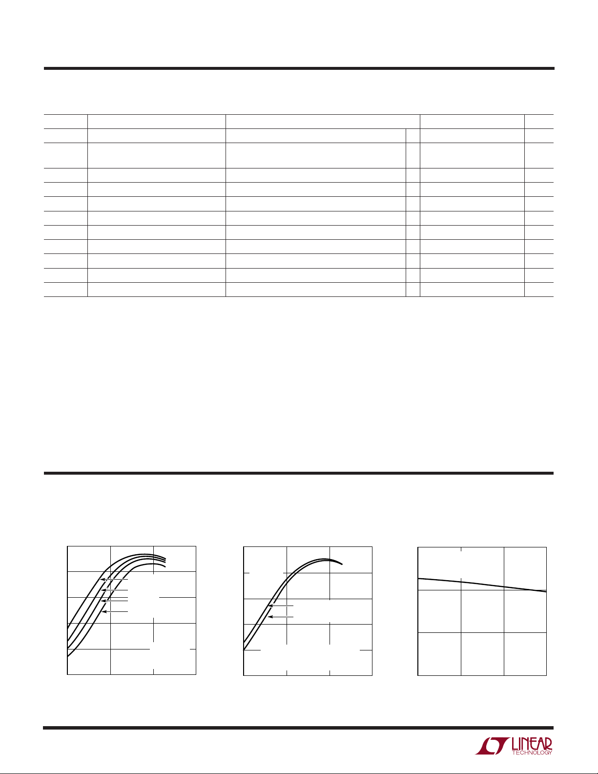
TYPICAL PERFOR A CE CHARACTERISTICS
Efficiency vs Output Current
(Figure 12)
100
80
60
40
EFFICIENCY (%)
20
0
0.1 1 10 100
VIN = 5V
VIN = 8V
VIN = 12V
VIN = 20V
V
V
f = 200kHz
OUTPUT CURRENT (A)
OUT
EXTVCC
= 2V
= 0V
1709 G01
Efficiency vs Output Current
(Figure 12)
100
V
= 2V
OUT
= 12V
V
IN
f = 200kHz
80
60
40
EFFICIENCY (%)
20
0
0.1
INTERNAL LDO VS EXTERNALLY
APPLIED 5V OVERALL EFFICIENCY
(FIGURE 12)
V
EXTVCC
V
EXTVCC
1 10 100
OUTPUT CURRENT (A)
= 5V
= 0V
4
1709 G02
Efficiency vs Input Voltage
(Figure 12)
100
V
= 3.3V
OUT
= 5V
V
EXTVCC
= 20A
I
OUT
90
EFFICIENCY (%)
80
70
5
10 15 20
VIN (V)
1709 G03
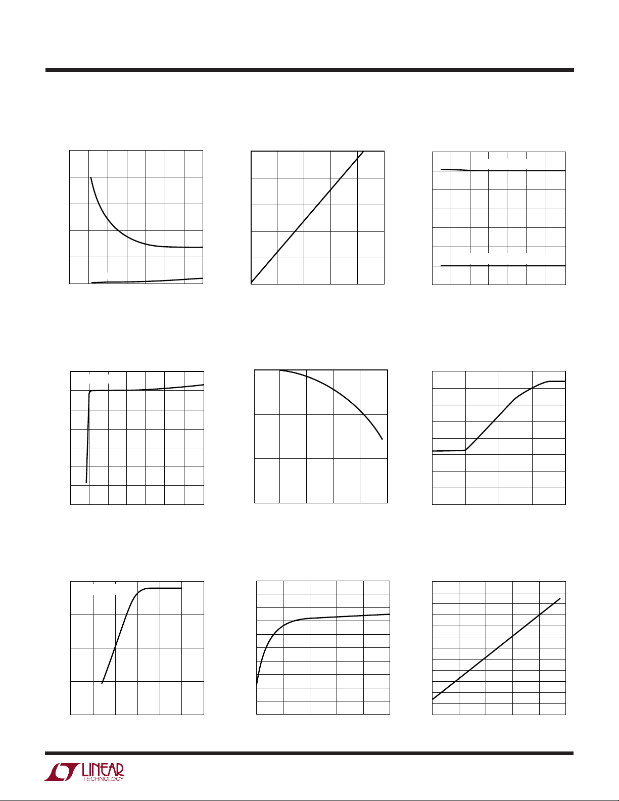
UW
TEMPERATURE (°C)
–50
INTV
CC
AND EXTV
CC
SWITCH VOLTAGE (V)
4.95
5.00
5.05
25 75
1709 G06
4.90
4.85
–25 0
50 100 125
4.80
4.70
4.75
INTVCC VOLTAGE
EXTVCC SWITCHOVER THRESHOLD
TYPICAL PERFOR A CE CHARACTERISTICS
LTC1709
Supply Current vs Input Voltage
and Mode EXTVCC Voltage Drop
1000
800
600
400
SUPPLY CURRENT (µA)
200
0
05
ON
SHUTDOWN
15
10
INPUT VOLTAGE (V)
20
25
30
35
1709 G04
250
200
150
100
VOLTAGE DROP (mV)
CC
EXTV
50
0
10
0
Maximum Current Sense Threshold
Internal 5V LDO Line Reg
5.1
I
= 1mA
LOAD
5.0
4.9
4.8
VOLTAGE (V)
4.7
CC
INTV
4.6
4.5
4.4
0
510
15 25
INPUT VOLTAGE (V)
20 30 35
1709 G07
vs Duty Factor
75
50
(mV)
SENSE
V
25
0
0
20 40 60 80
30
20
CURRENT (mA)
DUTY FACTOR (%)
INTVCC and EXTVCC Switch
Voltage vs Temperature
40
50
1709 G05
Maximum Current Sense Threshold
vs Percent of Nominal Output
Voltage (Foldback)
80
70
60
50
(mV)
40
SENSE
V
30
20
10
100
1709 G08
0
0
PERCENT ON NOMINAL OUTPUT VOLTAGE (%)
25
50
75
100
1709 G09
80
60
(mV)
40
SENSE
V
20
0
Maximum Current Sense Threshold
vs V
V
SENSE(CM)
0
(Soft-Start)
RUN/SS
= 1.6V
1234
V
(V)
RUN/SS
56
1709 G10
Maximum Current Sense Threshold
vs Sense Common Mode Voltage
80
76
72
(mV)
SENSE
68
V
64
60
1
0
COMMON MODE VOLTAGE (V)
3
2
Current Sense Threshold
vs ITH Voltage
90
80
70
60
50
40
(mV)
30
20
SENSE
V
10
0
–10
–20
4
1709 G11
–30
5
0.5
0
1.5
2
1
V
(V)
ITH
2.5
1709 G12
5
LTC1709
TEMPERATURE (°C)
–50 –25
0
EXTV
CC
SWITCH RESISTANCE (Ω)
4
10
0
50
75
1709 G22
2
8
6
25
100
125
UW
TYPICAL PERFOR A CE CHARACTERISTICS
Load Regulation V
0.0
–0.1
(%)
OUT
–0.2
NORMALIZED V
–0.3
–0.4
0
1
2
LOAD CURRENT (A)
FCB = 0V
V
= 15V
IN
FIGURE 1
3
4
5
1709 G13
Maximum Current Sense
Threshold vs Temperature
80
78
76
(mV)
SENSE
74
V
72
70
–50 –25
50
25
0
TEMPERATURE (°C)
75
100
125
1709 G17
vs V
ITH
RUN/SS
2.5
V
= 0.7V
OSENSE
2.0
1.5
(V)
ITH
V
1.0
0.5
0
0
234
1
V
RUN/SS
(V)
RUN/SS Current vs Temperature
1.8
1.6
1.4
1.2
1.0
0.8
0.6
RUN/SS CURRENT (µA)
0.4
0.2
0
–50 –25
0 25 125
TEMPERATURE (°C)
56
75 10050
1709 G14
1709 G18
SENSE Pins Total Source Current
100
50
(µA)
0
SENSE
I
–50
–100
0
24
V
COMMON MODE VOLTAGE (V)
SENSE
Soft-Start Up (Figure 12)
V
ITH
1V/DIV
V
OUT
2V/DIV
V
RUNSS
2V/DIV
100ms/DIV
6
1709 G15
1629 G19
V
OUT
50mV/DIV
I
OUT
10A/DIV
6
Load Step Response Using Active
Voltage Positioning (Figure 12)
20A
0A
20µs/DIV
1709 G20
Current Sense Pin Input Current
vs Temperature
35
EXTVCC = 5V
33
31
29
27
CURRENT SENSE INPUT CURRENT (µA)
25
–50 –25
0
TEMPERATURE (°C)
50
25
EXTVCC Switch Resistance
vs Temperature
100
125
1709 G21
75
UW
TYPICAL PERFOR A CE CHARACTERISTICS
LTC1709
Oscillator Frequency
vs Temperature
350
300
250
200
150
FREQUENCY (kHz)
100
50
0
–50
–25 0
V
= 5V
FREQSET
V
= OPEN
FREQSET
V
= 0V
FREQSET
50 100 125
25 75
TEMPERATURE (°C)
1709 G23
Undervoltage Lockout
vs Temperature
3.50
3.45
3.40
3.35
3.30
UNDERVOLTAGE LOCKOUT (V)
3.25
3.20
–50
–25 0
TEMPERATURE (°C)
UUU
PI FU CTIO S
RUN/SS (Pin 1): Combination of Soft-Start, Run Control
Input and Short-Circuit Detection Timer. A capacitor to
ground at this pin sets the ramp time to full current output.
Forcing this pin below 0.8V causes the IC to shut down all
internal circuitry. All functions are disabled in shutdown.
SENSE 1+, SENSE 2+ (Pins 2,14): The (+) Input to Each
Differential Current Comparator. The ITH pin voltage and
built-in offsets between SENSE– and SENSE+ pins in
conjunction with R
SENSE 1–, SENSE 2– (Pins 3, 13): The (–) Input to the
Differential Current Comparators.
EAIN (Pin 4): Input to the Error Amplifier that compares
the feedback voltage to the internal 0.8V reference voltage.
This pin is normally connected to a resistive divider from
the output of the differential amplifier (DIFFOUT).
PLLFLTR (Pin 5): The Phase-Locked Loop’s Low Pass
Filter is tied to this pin. Alternatively, this pin can be driven
with an AC or DC voltage source to vary the frequency of
the internal oscillator.
PLLIN (Pin 6): External Synchronization Input to Phase
Detector. This pin is internally terminated to SGND with
50kΩ. The phase-locked loop will force the rising top gate
signal of controller 1 to be synchronized with the rising
edge of the PLLIN signal.
set the current trip threshold.
SENSE
V
Shutdown Latch
RUN/SS
Thresholds vs Temperature
4.5
LATCH ARMING
LATCHOFF
THRESHOLD
0 25 125
TEMPERATURE (°C)
75 10050
1709 G25
50 100 125
25 75
1709 G24
4.0
3.5
3.0
2.5
2.0
1.5
1.0
0.5
SHUTDOWN LATCH THRESHOLDS (V)
0
–50 –25
NC (Pins 7, 36): Do not connect.
ITH (Pin 8): Error Amplifier Output and Switching Regula-
tor Compensation Point. Both current comparator’s thresholds increase with this control voltage. The normal voltage
range of this pin is from 0V to 2.4V
SGND (Pin 9): Signal Ground, common to both controllers. Route separately to the PGND pin.
V
DIFFOUT
(Pin 10): Output of a Differential Amplifier that
provides true remote output voltage sensing. This pin
normally drives an external resistive divider that sets the
output voltage.
–
V
OS
+
, V
(Pins 11, 12): Inputs to an Operational Ampli-
OS
fier. Internal precision resistors capable of being electronically switched in or out can configure it as a differential amplifier or an uncommitted Op Amp.
ATTENOUT (Pin 15): Voltage Feedback Signal Resistively
Divided According to the VID Programming Code.
ATTENIN (Pin 16): The Input to the VID Controlled Resistive Divider.
VID0–VID4 (Pins 17,18, 19, 20, 21): VID Control Logic
Input Pins.
V
(Pin 22): Supply Pin for the VID Control Circuit.
BIAS
7

LTC1709
PI FU CTIO S
UUU
AMPMD (Pin 23): This Logic Input pin controls the
connections of internal precision resistors that configure
the operational amplifier as a unity-gain differential
amplifier.
TG2, TG1 (Pins 24, 35): High Current Gate Drives for Top
N-Channel MOSFETS. These are the outputs of floating
drivers with a voltage swing equal to INTVCC superimposed on the switch node voltage SW.
SW2, SW1 (Pins 25, 34): Switch Node Connections to
Inductors. Voltage swing at these pins is from a Schottky
diode (external) voltage drop below ground to VIN.
BOOST 2, BOOST 1 (Pins 26, 33): Bootstrapped Supplies
to the Topside Floating Drivers. External capacitors are
connected between the Boost and Switch pins, and Schottky
diodes are connected between the Boost and INTVCC pins.
BG2, BG1 (Pins 27, 31): High Current Gate Drives for
Bottom N-Channel MOSFETS. Voltage swing at these pins
is from ground to INTVCC.
PGND (Pin 28): Driver Power Ground, connect to sources
of bottom N-channel MOSFETS and the (–) terminals of
CIN.
INTVCC (Pin 29): Output of the Internal 5V Linear Low
Dropout Regulator and the EXTVCC Switch. The driver and
control circuits are powered from this voltage source.
Decouple to power ground with a 1µF ceramic capacitor
placed directly adjacent to the IC and minimum of 4.7µF
additional tantalum or other low ESR capacitor.
EXTVCC (Pin 30): External Power Input to an Internal
Switch . This switch closes and supplies INTV
ing the internal low dropout regulator whenever EXTVCC is
higher than 4.7V. See EXTVCC Connection in the Applications Information section. Do not exceed 7V on this pin
and ensure V
VIN (Pin 32): Main Supply Pin. Should be closely decoupled
to the IC’s signal ground pin.
EXTVCC
≤ VIN.
bypass-
CC,
8
LTC1709
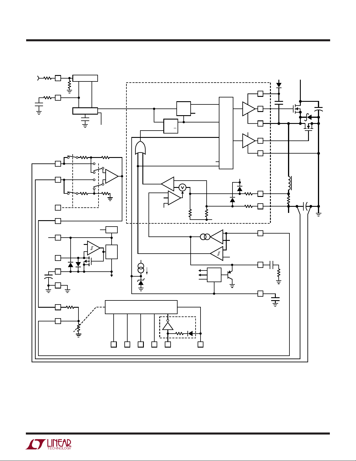
UU
W
FU CTIO AL DIAGRA
PLLIN
F
IN
R
LP
C
LP
PLLFLTR
V
OS
V
OS
AMPMD
DIFFOUT
V
IN
V
IN
EXTV
INTV
5V
+
SGND
PHASE DET
50k
0.8V
+
–
CLK1
CLK2
TO
SECOND
CHANNEL
A1
–
+
V
REF
5V
LDO
REG
INTERNAL
SUPPLY
OSCILLATOR
–
+
0V POSITION
4.7V
CC
CC
DUPLICATE FOR
SECOND CHANNEL
V
IN
1.2µA
6V
4(VFB)
I1
SLOPE
COMP
SRQ
INTV
BOOST
INTV
CC
30k
30k
CC
TG
SW
BG
PGND*
SENSE
SENSE
EAIN
I
TH
RUN/SS
+
–
R
SENSE
C
C
DROP
OUT
DET
BOT
FORCE BOT
Q
SHDN
–
+–
+
45k
SHDN
RST
4(VFB)
45k
2.4V
RUN
SOFT-
START
EA
OV
SWITCH
LOGIC
–
+
+
–
TOP
BOT
INTV
V
FB
0.80V
0.86V
V
CC
IN
D
B
C
B
L
+
C
IN
C
OUT
+
V
OUT
R
C
ATTENIN
ATTENOUT
R2
20k
R1 R1 VARIABLE
5-BIT VID DECODER
VID0 VID1 VID2 VID4
VID3
TYPICAL ALL
VID PINS
40k
C
SS
V
BIAS
1709 FBD
9
 Loading...