

Linear Technology LTC1708-PG Datasheet
LTC1708-PG
Final Electrical Specifications
Dual Adjustable 5-Bit VID
High Efficiency, 2-Phase Current Mode
Synchronous Buck Regulator Controller
FEATURES
■
Out-of-Phase Controllers Reduce Input Capacitance
and Power Supply Induced Noise
■
OPTI-LOOPTM Compensation Minimizes C
■
Power Good Output Monitors Both Outputs
■
5-Bit Mobile VID Control, V
■
Dual N-Channel MOSFET Synchronous Drive
■
±1% Output Voltage Accuracy
■
DC Programmed Fixed Frequency 150kHz to 300kHz
■
Wide VIN Range: 3.5V to 36V Operation
■
Very Low Dropout Operation: 99% Duty Cycle
■
Adjustable Soft-Start Current Ramping
■
Foldback Output Current Limiting
■
Latched Short-Circuit Shutdown with Defeat Option
■
Output Overvoltage Protection
■
Remote Output Voltage Sense
■
Low Shutdown Current: 20µA
■
5V and 3.3V Standby Regulators
■
Selectable Constant Frequency, Burst ModeTM and
: 0.9V to 2.0V
OUT
OUT
Continuous Operation
U
APPLICATIO S
■
Notebook and Palmtop Computers, PDAs
■
Portable Instruments
U
February 2000
DESCRIPTIO
The LTC®1708 is a dual adjustable 5-bit VID programmable step-down switching regulator controller that drives
all N-Channel power MOSFET stages. A constant frequency current mode architecture allows adjustment of
the frequency up to 300kHz. Power loss and noise due to
the ESR of the input capacitance are minimized by operating the two main controller output stages out of phase.
OPTI-LOOP compensation allows the transient response
to be optimized over a wide range of output capacitance
and ESR values. The precision 0.8V reference is compatible with future microprocessor generations, and a wide
3.5V to 30V (36V maximum) input supply range that
encompasses all battery chemistries. A power good output indicates when the output voltages are within 7.5% of
their programmed value.
A RUN/SS pin for each controller provides both soft-start
and an optional timed, short-circuit shutdown. Other
protection features include: internal foldback current limiting and an output overvoltage crowbar. The force continuous control pin (FCB) can be used to inhibit Burst
Mode operation or to regulate a third, flyback output.
, LTC and LT are registered trademarks of Linear Technology Corporation.
Burst Mode and OPTI-LOOP are trademarks of Linear Technology Corporation.
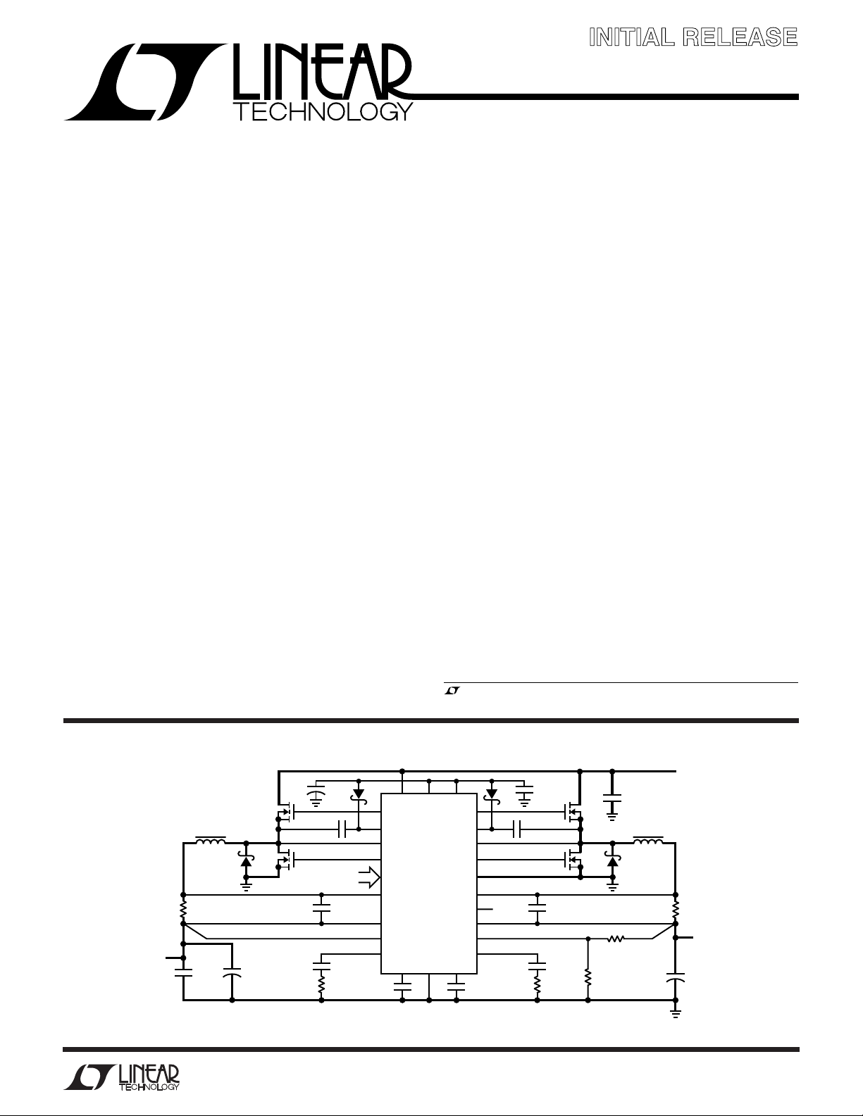
TYPICAL APPLICATIO
R
SENSE1
0.003Ω
V
OUT1
0.925V TO
2.00V
14.1A
C
10µF
6.3V
CERAMIC
U
+
4.7µF
D3
1µH
OUT1a
VINVIDVCCINTV
L1
M1
M2
D1
C
OUT1
+
270µF
2V
SP
×4
C
B1
0.47µF
5 VID BITS
1000pF
C
1500pF
R
C1
22k
C1
TG1 TG2
BOOST1 BOOST2
SW1 SW2
LTC1708-PG
BG1 BG2
VID0 TO VID4 PGND
+
SENSE1
–
SENSE1
ATTNIN V
I
TH1
RUN/SS1 RUN/SS2SGND
C
SS1
0.1µF
SENSE2
PGOOD
SENSE2
OSENSE2
CC
+
–
I
TH2
C
SS2
0.1µF
Figure 1. High Efficiency VID Controlled, 2-Output Step-Down Converter
Information furnished by Linear Technology Corporation is believed to be accurate and reliable.
However, no responsibility is assumed for its use. Linear Technology Corporation makes no representation that the interconnection of its circuits as described herein will not infringe on existing patent rights.
D4
C
220pF
C2
R
15k
C
B2
C2
1µF
CERAMIC
0.1µF
1000pF
20k
1%
V
IN
L2
R
SENSE2
C
180µF
0.01Ω
OUT
4V
SP
4.75V TO 28V
V
OUT2
1.5V
4A
M1: IRF7811
+
M2: 1RF7809
M3a, M3b: FDS6982
L1: VISHAY 5050CE
ATTNOUT CONNECTED TO EAIN1
1628 F01
C
IN
10µF
50V
CERAMIC
M3a
×4
2.2µH
M3b
D2
R4
63.4k
1%
R3
1
LTC1708-PG
WW
W
U
ABSOLUTE AXI U RATI GS
(Note 1)
Input Supply Voltage (VIN).........................36V to –0.3V
Topside Driver Voltages
(BOOST1, BOOST2) ...................................42V to –0.3V
Switch Voltage (SW1, SW2) .........................36V to – 5V
INTV
(BOOST1-SW1), (BOOST2-SW2), ...............7V to –0.3V
SENSE1+, SENSE2+, SENSE1–,
SENSE2– Voltages....................... (1.1)INTVCC to –0.3V
FREQSET, STBYMD, FCB, VIDVCC, VID0-4,
PGOOD Voltages..........................................7V to –0.3V
I
TH1, ITH2
ATTNOUT Voltages ...................................2.7V to –0.3V
Peak Output Current <10µs (TG1, TG2, BG1, BG2) ... 3A
INTVCC Peak Output Current ................................ 50mA
Operating Ambient Temperature Range
(Note 2) ...................................................–40°C to 85°C
Junction Temperature (Note 3)............................. 125°C
Storage Temperature Range ................. –65°C to 150°C
Lead Temperature (Soldering, 10 sec)..................300°C
EXTVCC, RUN/SS1, RUN/SS2,
CC,
, EAIN1, EAIN2, ATTNIN,
UUW
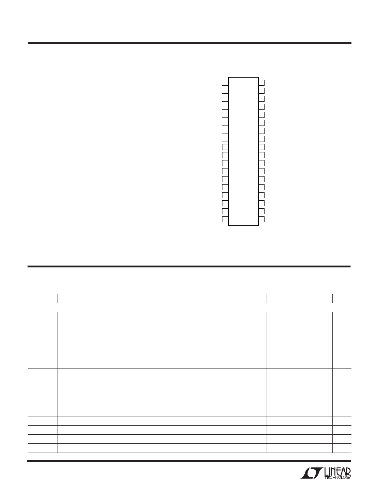
PACKAGE/ORDER I FOR ATIO
TOP VIEW
RUN/SS1
SENSE1
SENSE1
EAIN1
FREQSET
STBYMD
FCB
I
TH1
SGND
3.3V
OUT
I
TH2
EAIN2
SENSE2
SENSE2
ATTNOUT
ATTNIN
VID0
VID1
1
+
2
–
3
4
5
6
7
8
9
10
11
12
–
13
+
14
15
16
17
18
G PACKAGE
36-LEAD PLASTIC SSOP
T
= 125°C, θJA = 85°C/W
JMAX
36
35
34
33
32
31
30
29
28
27
26
25
24
23
22
21
20
19
PGOOD
TG1
SW1
BOOST1
V
IN
BG1
EXTV
CC
INTV
CC
PGND
BG2
BOOST2
SW2
TG2
RUN/SS2
VIDV
CC
VID4
VID3
VID2
Consult factory for Industrial and Military grade parts.
ORDER PART
NUMBER
LTC1708EG-PG
ELECTRICAL CHARACTERISTICS
temperature range, otherwise specifications are at TA = 25°C. VIN = 15V, V
The ● denotes the specifications which apply over the full operating
RUN/SS1, 2
= 5V unless otherwise noted.
SYMBOL PARAMETER CONDITIONS MIN TYP MAX UNITS
Main Control Loops
V
EAIN1, 2
Regulated Feedback Voltage (Note 4); I
Voltage = 1.2V ● 0.792 0.800 0.808 V
TH1, 2
at EAIN Pin
I
EAIN1, 2
V
REFLNREG
V
LOADREG
g
m1, 2
g
mOL1, 2
I
Q
V
FCB
I
FCB
V
BINHIBIT
Feedback Current (Note 4) –5 – 50 nA
Reference Voltage Line Regulation VIN = 3.6V to 30V (Note 4) 0.002 0.02 %/V
Output Voltage Load Regulation (Note 4)
Transconductance Amplifier g
m
Transconductance Amplifier GBW I
Measured in Servo Loop; I
Measured in Servo Loop; I
I
= 1.2V; Sink/Source 5µA; (Note 4) 1.3 mmho
TH1, 2
= 1.2V; (gm • ZL, No Ext Load) (Note 4) 3 MHz
TH1, 2
Voltage = 1.2V to 0.7V ● 0.1 0.5 %
TH1, 2
Voltage = 1.2V to 2.0V ● –0.1 –0.5 %
TH1, 2
Input DC Supply Current (Note 5)
Normal Mode EXTV
Standby V
Shutdown V
Tied to GND; VID Inputs Open Circuit 850 µA
CC
RUN/SS1, 2
RUN/SS1, 2
= 0V, V
= 0V, V
> 2V 125 µA
STBYMD
= Open 20 35 µA
STBYMD
Forced Continuous Threshold ● 0.760 0.800 0.840 V
Forced Continuous Current V
= 0.85V –0.3 – 0.18 – 0.1 µA
FCB
Burst Inhibit Threshold Measured at FCB pin 4.3 4.8 V
UVLO Undervoltage Lockout VIN Ramping Down 3.5 4 V
2
LTC1708-PG
ELECTRICAL CHARACTERISTICS
temperature range, otherwise specifications are at TA = 25°C. VIN = 15V, V
The ● denotes the specifications which apply over the full operating
RUN/SS1, 2
= 5V unless otherwise noted.
SYMBOL PARAMETER CONDITIONS MIN TYP MAX UNITS
V
OV
I
SENSE
V
STBYMD
V
STBYMD
DF
MAX
I
RUN/SS1, 2
V
RUN/SS1, 2
V
RUN/SS1, 2
I
SCL1, 2
I
SDLHO
V
SENSE(MAX)
Output Overvoltage Threshold Measured at EAIN1, 2 0.84 0.86 0.88 V
Sense Pins Total Source Current (Each Channel); V
MS Master Shutdown Threshold V
KA Keep-Alive Power On-Threshold V
SENSE1–, 2–
Ramping Down 0.4 0.6 V
STBYMD
Ramping Up, RUN
STBYMD
= V
SENSE1+, 2+
= 0V 1.5 2 V
SS1, 2
= 0V –85 –60 µA
Maximum Duty Factor In Dropout 98 99.4 %
Soft-Start Charge Current V
ON RUN/SS Pin ON Threshold V
LT RUN/SS Pin Latchoff Threshold V
RUN/SS1, 2
RUN/SS1, VRUN/SS2
RUN/SS1, VRUN/SS2
RUN/SS Discharge Current Soft Short Condition E
V
RUN/SS1, 2
= 1.9V 0.5 1.2 µA
Rising 1.0 1.5 1.9 V
Rising from 3V 4.1 4.5 V
= 0.5V; 0.5 2 4 µA
AIN1, 2
= 4.5V
Shutdown Latch Disable Current EAIN1, 2 = 0.5V 1.6 5 µA
Maximum Current Sense Threshold V
EAIN1, 2
V
EAIN1, 2
= 0.7V; V
= 0.7V; V
= 5V 65 75 85 mV
SENSE1, 2
= 5V ● 62 75 88 mV
SENSE1, 2
TG Transition Time:
TG1, 2 t
TG1, 2 t
r
f
Rise Time C
Fall Time C
= 3300pF (Note 10) 50 90 ns
LOAD
= 3300pF (Note 10) 50 90 ns
LOAD
BG Transition Time:
BG1, 2 t
BG1, 2 t
TG/BG t
r
f
1D
Rise Time C
Fall Time C
Top Gate Off to Bottom Gate On Delay C
= 3300pF (Note 10) 40 90 ns
LOAD
= 3300pF (Note 10) 40 80 ns
LOAD
= 3300pF Each Driver (Note 10) 90 ns
LOAD
Synchronous Switch-On Delay Time
BG/TG t
2D
Bottom Gate Off to Top Gate On Delay C
= 3300pF Each Driver (Note 10) 90 ns
LOAD
Top Switch-On Delay Time
t
ON(MIN)
Minimum On-Time Tested with a Square Wave (Notes 6, 10) 160 200 ns
INTVCC Linear Regulator
V
INTVCC
V
INT INTVCC Load Regulation ICC = 0 to 20mA, V
LDO
V
EXT EXTVCC Voltage Drop ICC = 20mA, V
LDO
V
EXTVCC
V
LDOHYS
Internal VCC Voltage 6V < VIN < 30V, V
EXTVCC
EXTVCC Switchover Voltage ICC = 20mA, EXTV
= 4V 4.8 5.0 5.2 V
EXTVCC
= 4V 0.2 1.0 %
EXTVCC
= 5V 120 240 mV
Ramping Positive ● 4.5 4.7 V
CC
EXTVCC Hysteresis 0.2 V
Oscillator
f
OSC
f
LOW
f
HIGH
I
FREQSET
Oscillator Frequency V
Lowest Frequency V
Highest Frequency V
FREQSET Input Current V
= Open (Note 7) 190 220 250 kHz
FREQSET
= 0V 120 140 170 kHz
FREQSET
= 2.4V 280 310 350 kHz
FREQSET
= 0V –2 – 1 µA
FREQSET
3.3V Linear Regulator
V
3.3OUT
V
3.3IL
V
3.3VL
3.3V Regulator Output Voltage No Load ● 3.25 3.35 3.45 V
3.3V Regulator Load Regulation I
3.3V Regulator Line Regulation 6V < V
= 0 to 10mA 0.5 2 %
3.3
< 30V 0.05 0.2 %
IN
PGOOD Output
V
PGL
I
PGOOD
V
PG
PGOOD Voltage Low I
PGOOD Leakage Current V
= 2mA 0.1 0.3 V
PGOOD
= 5V 1 µA
PGOOD
PGOOD Trip Level Relative to the 0.8V Regulated Feedback Voltage
EAIN1, 2 Ramping Negative from 0.8V – 10 –7.5 – 5 %
EAIN1, 2 Ramping Positive from 0.8V 5 7.5 10 %
3
LTC1708-PG
ELECTRICAL CHARACTERISTICS
temperature range, otherwise specifications are at TA = 25°C. VIN = 15V, V
The ● denotes the specifications which apply over the full operating
RUN/SS1, 2
= 5V unless otherwise noted.
SYMBOL PARAMETER CONDITIONS MIN TYP MAX UNITS
VID Parameters
VIDV
CC
I
VIDVCC
R
FBOUT1/SENSE1
R
RATIO
R
PULL-UP
V
IDT
I
VIDLEAK
V
PULL-UP
Note 1: Absolute Maximum Ratings are those values beyond which the life
of a device may be impaired.
Note 2: The LTC1708EG-PG is guaranteed to meet performance
specifications from 0°C to 70°C. Specifications over the –40°C to 85°C
operating temperature range are assured by design, characterization and
correlation with statistical process controls.
Note 3: T
dissipation P
LTC1708EG-PG: T
Note 4: The LTC1708-PG is tested in a feedback loop that servos V
to a specified voltage and measures the resultant EAIN1, 2.
Note 5: The supply current is higher due to the gate charge being delivered
at the switching frequency. See Applications Information.
VID Operating Supply Voltage 2.7 5.5 V
VID Supply Current VIDVCC = 3.3V (Note 8) 0.01 5 µA
Resistance Between ATTNIN/ATTNOUT 10 5 kΩ
Resistor Ratio Accuracy Programmed from 0.925V to 2.00V 0.25 %
VID0 to VID4 Pull-Up Resistance (Note 9) V
= 0.7V 40 kΩ
DIODE
VID Voltage Threshold 0.4 1.0 1.6 V
VID Input Leakage Current (Note 9) VIDVCC < VIDVCC < 7V 0.1 1 µA
VID Pull-Up Voltage VIDVCC = 3V 2.5 2.8 3.1 V
Note 6: The minimum on-time condition corresponds to the on inductor
peak-to-peak ripple current ≥40% of I
(see minimum on-time
MAX
considerations in the Applications Information section).
Note 7: V
pin internally tied to 1.19V reference through a large
FREQSET
resistance.
Note 8: With all five VID inputs floating (or tied to VIDV
is calculated from the ambient temperature TA and power
J
according to the following formulas:
D
= TA + (PD • 85°C/W)
J
ITH1, 2
current is typically <1µA. However, the VIDVCC current will rise and be
approximately equal to the number of grounded VID input pins times
– 0.6V)/40k. (See the Applications Information section.)
(VIDV
CC
Note 9: Each built-in pull-up resistor attached to the VID inputs also has a
series diode to allow input voltages higher than the VIDV
damage or clamping. (See Applications Information section.)
Note 10: Rise and fall times are measured at 20% to 80% levels. Delay
) the VIDV
CC
supply without
CC
CC
and nonoverlap times are measured using 50% levels.
UW
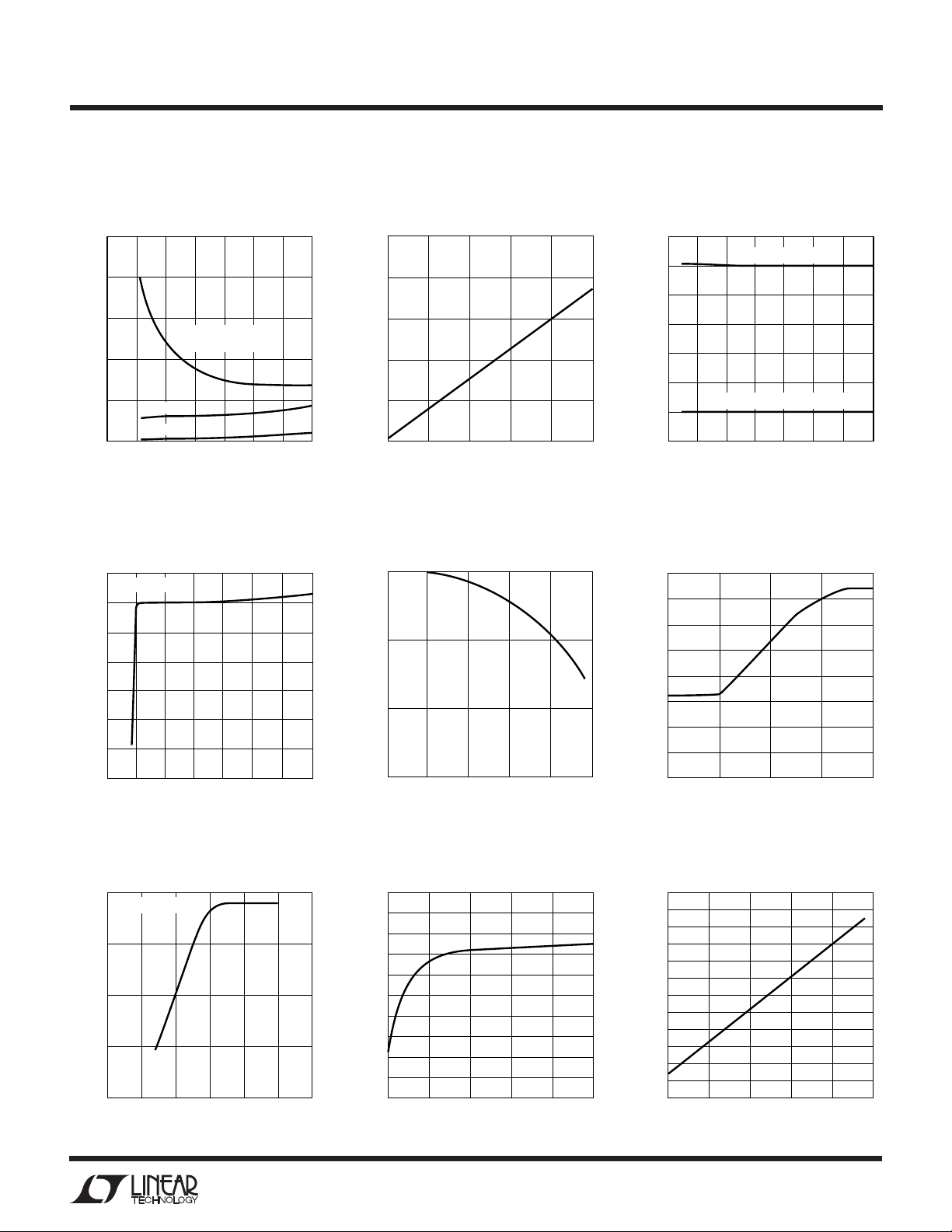
TYPICAL PERFOR A CE CHARACTERISTICS
Efficiency vs Output Current
and Mode (Figure 12)
100
90
Burst Mode
OPERATION
80
70
60
50
40
EFFICIENCY (%)
30
20
10
0
0.1
CONSTANT FREQUENCY
MODE
PWM MODE
1
OUTPUT CURRENT (A)
10
15A
VIN = 15V
= 1.6V
V
OUT
100
1708 G01
Efficiency vs Output Current
(Figure 12)
100
90
80
70
60
50
40
EFFICIENCY (%)
30
20
10
0
0.01
EXTV
V
IN
= 0V
CC
= 5V
VIN = 10V
V
= 15V
IN
VIN = 20V
0.1
OUTPUT CURRENT (A)
1
V
V
FCB
OUT
10
15A
= OPEN
= 1.6V
1708 G02
100
Efficiency vs Input Voltage
(Figure 12)
100
V
= 1.6V
OUT
= 0V
EXTV
CC
90
80
70
EFFICIENCY (%)
60
50
510
15 20
INPUT VOLTAGE (V)
I
I
OUT
OUT
= 7A
= 12A
25
1708 G03
28
4
UW
TEMPERATURE (°C)
–50
INTV
CC
AND EXTV
CC
SWITCH VOLTAGE (V)
4.95
5.00
5.05
25 75
1708 G06
4.90
4.85
–25 0
50 100 125
4.80
4.70
4.75
INTVCC VOLTAGE
EXTVCC SWITCHOVER THRESHOLD
TYPICAL PERFOR A CE CHARACTERISTICS
LTC1708-PG
Supply Current vs Input Voltage
and Mode (Figure 12)
1000
800
600
400
SUPPLY CURRENT (µA)
200
0
05
BOTH
CONTROLLERS ON
STANDBY
SHUTDOWN
10
INPUT VOLTAGE (V)
20
15
Internal 5V LDO Line Reg
5.1
I
= 1mA
LOAD
5.0
4.9
4.8
VOLTAGE (V)
4.7
CC
INTV
4.6
4.5
4.4
0
510
INPUT VOLTAGE (V)
20 30 35
15 25
INTVCC and EXTVCC Switch
EXTVCC Voltage Drop
250
200
150
100
VOLTAGE DROP (mV)
CC
EXTV
50
30
35
1708 G04
25
0
10
0
CURRENT (mA)
30
40
20
50
1708 G05
Voltage vs Temperature
Maximum Current Sense Threshold
1708 G07
Maximum Current Sense Threshold
vs Duty Factor
75
50
(mV)
SENSE
V
25
0
0
20 40 60 80
DUTY FACTOR (%)
100
1708 G08
vs Percent of Nominal Output
Voltage (Foldback)
80
70
60
50
(mV)
40
SENSE
V
30
20
10
0
0
25
PERCENT ON NOMINAL OUTPUT VOLTAGE (%)
50
75
100
1708 G09
80
60
(mV)
40
SENSE
V
20
0
Maximum Current Sense Threshold
vs V
V
SENSE(CM)
0
(Soft-Start)
RUN/SS
= 1.6V
1234
V
(V)
RUN/SS
56
1708 G10
Maximum Current Sense Threshold
vs Sense Common Mode Voltage
80
76
72
(mV)
SENSE
68
V
64
60
1
0
2
COMMON MODE VOLTAGE (V)
3
Current Sense Threshold
vs ITH Voltage
90
80
70
60
50
40
(mV)
30
20
SENSE
V
10
0
–10
–20
4
5
1708 G11
–30
0.5
0
1.5
2
1
V
(V)
ITH
2.5
1708 G12
5

LTC1708-PG
UW
TYPICAL PERFOR A CE CHARACTERISTICS
Load Regulation
0.0
–0.1
(%)
OUT
–0.2
NORMALIZED V
–0.3
–0.4
0
1
2
LOAD CURRENT (A)
FCB = 0V
= 15V
V
IN
FIGURE 1
V
OUT2
3
4
5
1708 G13
(V)
ITH
V
2.5
2.0
1.5
1.0
0.5
V
vs V
ITH
RUN/SS
V
= 0.7V
EAIN
0
0
234
1
V
RUN/SS
(V)
Maximum Current Sense
Threshold vs Temperature Dropout Voltage vs Output Current
80
78
76
(mV)
SENSE
74
V
72
70
–50 –25
50
25
0
TEMPERATURE (°C)
100
125
1708 G17
75
4
V
= 5V
OUT
3
2
DROPOUT VOLTAGE (V)
1
0
0
0.5 1.0 1.5 2.0
OUTPUT CURRENT (A)
R
SENSE
R
= 0.015Ω
SENSE
= 0.010Ω
2.5 3.0 3.5 4.0
56
1708 G14
1708 G18
SENSE Pins Total Source Current
100
50
(µA)
0
SENSE
I
–50
–100
0
24
V
COMMON MODE VOLTAGE (V)
SENSE
RUN/SS Current vs Temperature
1.8
1.6
1.4
1.2
1.0
0.8
0.6
RUN/SS CURRENT (µA)
0.4
0.2
0
–50 –25
0 25 125
TEMPERATURE (°C)
6
1708 G15
75 10050
1708 G25
V
OUT
100mV/DIV
I
OUT
5A/DIV
6
Load Step (Figure 12)
= 15V 10µs/DIV 1708 G22
V
IN
V
= 1.6V
OUT2
LOAD STEP = 100mA – 15A
CONSTANT FREQUENCY MODE: V
ACTIVE VOLTAGE POSITIONING CIRCUIT
FCB
= V
INTVCC
V
OUT
100mV/DIV
I
OUT
5A/DIV
Load Step (Figure 12)
V
= 15V 10µs/DIV 1708 G20
IN
V
= 1.6V
OUT2
LOAD STEP = 100mA – 15A
Burst Mode OPERATION: V
ACTIVE VOLTAGE POSITIONING CIRCUIT
FCB
= OPEN
V
OUT
100mV/DIV
I
OUT
5A/DIV
Load Step (Figure 12)
VIN = 15V 10µs/DIV 1708 G21
V
= 1.6V
OUT2
LOAD STEP = 100mA – 15A
CONTINUOUS MODE: V
ACTIVE VOLTAGE POSITIONING CIRCUIT
FCB
= 0V
UW
TEMPERATURE (°C)
–50
200
250
350
25 75
1708 G28
150
100
–25 0
50 100 125
50
0
300
FREQUENCY (kHz)
V
FREQSET
= 5V
V
FREQSET
= OPEN
V
FREQSET
= 0V
TYPICAL PERFOR A CE CHARACTERISTICS
Soft-Start Up (Figure 12)
V
RUN/SS
2V/DIV
V
OUT
1V/DIV
I
OUT
5A/DIV
20mV/DIV
Burst Mode Operation (Figure 12)
V
OUT
I
OUT
5A/DIV
V
OUT
20mV/DIV
I
OUT
2A/DIV
LTC1708-PG
Constant Frequency (Burst Inhibit)
Operation (Figure 12)
CURRENT SENSE INPUT CURRENT (µA)
V
= 15V 100ms/DIV 1708 G19
IN
V
= 1.6V
OUT2
Current Sense Input Current
vs Temperature
35
33
31
29
27
25
–50 –25
0
TEMPERATURE (°C)
50
25
Undervoltage Lockout
vs Temperature
3.50
3.45
3.40
3.35
3.30
UNDERVOLTAGE LOCKOUT (V)
3.25
3.20
–50
–25 0
75
100
1708 G26
25 75
TEMPERATURE (°C)
10
8
6
4
SWITCH RESISTANCE (Ω)
CC
2
EXTV
125
50 100 125
0
V
= 15V 20µs/DIV 1708 G23
IN
V
= 1.6V
OUT2
= OPEN
V
FCB
I
= 250mA
OUT
EXTVCC Switch Resistance
vs Temperature
50
25
–50 –25
1708 G29
0
TEMPERATURE (°C)
75
V
IN
V
OUT2
V
FCB
I
OUT
Oscillator Frequency
vs Temperature
125
100
1708 G27
Shutdown Latch Thresholds
vs Temperature
4.5
4.0
3.5
3.0
2.5
2.0
1.5
1.0
0.5
SHUTDOWN LATCH THRESHOLDS (V)
0
–50 –25
LATCH ARMING
LATCHOFF
THRESHOLD
0 25 125
TEMPERATURE (°C)
= 15V 20µs/DIV 1708 G24
= 1.6V
= V
INTVCC
= 250mA
75 10050
1708 G30
7

LTC1708-PG
UUU
PI FU CTIO S
RUN/SS1, RUN/SS2 (Pins 1, 23): Combination of softstart, run control inputs and short-circuit detection timers.
A capacitor to ground at each of these pins sets the ramp
time to full output current. Forcing either of these pins
back below 1.0V causes the IC to shut down the circuitry
required for that particular controller. Latchoff overvoltage protection is also invoked via this pin as described in
the Applications Information section.
SENSE1+, SENSE2+ (Pins 2, 14): The (+) Input to the
Differential Current Comparators. The Ith pin voltage and
built-in offsets between the SENSE– and SENSE+ pins in
conjunction with R
SENSE1–, SENSE2– (Pins 3, 13): The (–) Input to the
Differential Current Comparators.
EAIN1, EAIN2 (Pins 4, 12): Receives the remotely sensed
feedback voltage for each controller from a resistive
divider across the output. The VID section may be used for
one resistive divider.
FREQSET (Pin 5): Frequency Control Input to the Oscillator. This pin can be left open, tied to ground, tied to INTV
or driven by an external voltage source. This pin can also
be used with an external phase detector to build a true
phase-locked loop.
STBYMD (Pin 6): Control pin that determines which circuitry remains active when the controllers are shut down
and/or provides a common control point to shut down
both controllers. See the Operation section for details.
FCB (Pin 7): Forced Continuous Control Input. This input
acts on both controllers and is normally used to regulate
a secondary winding using a resistive divider. An applied
input voltage below 0.8V will force continuous synchronous operation on both controllers. Do not leave this pin
floating.
I
TH1, ITH2
ing Regulator Compensation Point. Each associated channels’ current comparator trip point increases with this
control voltage.
SGND (Pin 9): Small-Signal Ground. Common to both
controllers, this pin must be routed separately from high
current grounds to the common (–) terminals of the
C
OUT
(Pins 8, 11): Error Amplifier Output and Switch-
capacitors.
sets the current trip threshold.
SENSE
CC
3.3V
supplying 10mA DC with peak currents as high as 50mA.
ATTNOUT (Pin 15): Divided down output voltage feeding
the EAIN pin of the regulator. The VID inputs program a
resistive divider between ATTNIN and SGND. ATTNOUT is
the tap point on the divider. The voltage on ATTNOUT is
0.8V when the output is in regulation. This pin can be
bypassed to SGND with 50pF.
ATTNIN (Pin 16): Receives the remotely sensed feedback
voltage from the output.
VID0 to VID4 (Pins 17 to 21): Digital inputs for controlling
the output voltage from 0.925V to 2.0V. Table 1 specifies
the output voltage for the 32 combinations of digital
inputs. The LSB (VID0) represents 50mV increments in
the upper voltage range (2.00V to 1.30V) and 25mV
increments in the lower voltage range (1.275V to 0.925V).
Logic Low = GND, Logic High = VIDVCC or Float.
VIDVCC (Pin 22): VID Input Supply Voltage. Range from
2.7V to 5.5V. Typically this pin is tied to INTVCC.
PGND (Pin 28): Driver Power Ground. Connects to the
sources of bottom (synchronous) N-channel MOSFETs, anode of the Schottky rectifier and the (–) terminal(s) of CIN.
INTVCC (Pin 29): Output of the Internal 5V Linear Low
Dropout Regulator and the EXTVCC Switch. The driver and
control circuits are powered from this voltage source. Must
be decoupled to power ground with a minimum of 4.7µF
tantalum or other low ESR capacitor. The INTVCC regulator
standby function is determined by the STBYMD pin.
EXTVCC (Pin 30): External Power Input to an Internal
Switch Connected to INTVCC. This switch closes and
supplies VCC power, bypassing the internal low dropout
regulator, whenever EXTVCC is higher than 4.7V. See
EXTVCC connection in Applications Information section.
Do not exceed 7V on this pin.
BG1, BG2 (Pins 31, 27): High Current Gate Drives for
Bottom (Synchronous) N-Channel MOSFETs. Voltage
swing at these pins is from ground to INTVCC.
VIN (Pin 32): Main Supply Pin. A bypass capacitor should
be tied between this pin and the signal ground pin.
(Pin 10): Output of a linear regulator capable of
OUT
8
UUU
PI FU CTIO S
LTC1708-PG
BOOST1, BOOST2 (Pins 33, 26): Bootstrapped Supplies
to the Topside Floating Drivers. Capacitors are connected
between the boost and switch pins and Schottky diodes
are tied between the boost and INTV
at the boost pins is from INTV
CC
pins. Voltage swing
CC
to (VIN + INTVCC).
SW1, SW2 (Pins 34, 25): Switch Node Connections to
Inductors. Voltage swing at these pins is from a Schottky
diode (external) voltage drop below ground to VIN.
UU
W
FU CTIO AL DIAGRA
V
V
SEC
IN
+
FREQSET
PGOOD
3.3V
EXTV
INTV
5V
STBYMD
ATTNIN
ATTNOUT
VARIABLE
FCB
V
SGND
0.17µA
OUT
IN
CC
CC
R1
1M
OSCILLATOR
4.5V
0.8V
+
–
4.8V
R2
10k
1.19V
CLK1
CLK2
–
+
–
+
–
+
–
+
–
+
+
–
V
REF
+
–
5-BIT VID DECODER
5V
LDO
REG
INTERNAL
SUPPLY
0.86V
V
0.74V
0.86V
V
0.74V
BINH
FCB
DUPLICATE FOR SECOND
CONTROLLER CHANNEL
DROP
OUT
FB1
SRQ
FB2
0.86V
4(VFB)
SLOPE
COMP
1.2µA
6V
40k
EACH VID
INPUT
DET
Q
+
0.6V
–
I
1
+
+– –+
–
45k
2.4V
4(VFB)
TG1, TG2 (Pins 35, 24): High Current Gate Drives for Top
N-Channel MOSFETs. These are the outputs of floating
drivers with a voltage swing equal to INTV
CC
– 0.5V
superimposed on the switch node voltage SW.
PGOOD (Pin 36): Open-Drain Logic Output. PGOOD is
pulled to ground when the voltage at either EAIN pin is not
within 7.5% of the setpoint.
V
CC
IN
D
B
C
B
D
SEC
C
C
R
C
C
C2
C
SS
D
R
1
SENSE
+
C
IN
C
OUT
+
+
C
SEC
SHDN
RST
BOT
3mV
TOP ON
FCB
SHDN
–
+
45k
OV
RUN
SOFTSTART
I
2
EA
SWITCH
LOGIC
–
+
+
–
V
FB
0.800V
0.860V
TOP
BOT
INTV
INTV
CC
30k
30k
CC
BOOST
TG
SW
BG
PGND
SENSE
SENSE
EAIN
I
TH
RUN/SS
INTV
+
–
V
OUT
VID0
VID1 VID2 VID3 VID4
VIDV
CC
1708 F02
Figure 2
9

LTC1708-PG
U
OPERATIO
(Refer to Functional Diagram)
Main Control Loop
The LTC1708 uses a constant frequency, current mode
step-down architecture with the two controller channels
operating 180 degrees out of phase. During normal operation, each top MOSFET is turned on when the clock for that
channel sets the RS latch, and turned off when the main
current comparator, I1, resets the RS latch. The peak
inductor current at which I1 resets the RS latch is controlled by the voltage on the I
each error amplifier EA. The EAIN pin receives the voltage
feedback signal, which is compared to the internal reference voltage by the EA. When the load current increases,
it causes a slight decrease in EAIN relative to the 0.8V
reference, which in turn causes the ITH voltage to increase
until the average inductor current matches the new load
current. After the top MOSFET has turned off, the bottom
MOSFET is turned on until either the inductor current
starts to reverse, as indicated by current comparator I2, or
the beginning of the next cycle.
The top MOSFET drivers are biased from floating bootstrap capacitor CB, which normally is recharged during
each off cycle through an external diode when the top
MOSFET turns off. As VIN decreases to a voltage close to
V
, the loop may enter dropout and attempt to turn on
OUT
the top MOSFET continuously. The dropout detector detects this and forces the top MOSFET off for about 500ns
every tenth cycle to allow CB to recharge.
The main control loop is shut down by pulling the RUN/SS
pin low. Releasing RUN/SS allows an internal 1.2µA
current source to charge soft-start capacitor CSS. When
CSS reaches 1.5V, the main control loop is enabled with the
ITH voltage clamped at approximately 30% of its maximum
value. As CSS continues to charge, the I
gradually released allowing normal, full-current operation. When both RUN/SS1 and RUN/SS2 are low, all
LTC1708 controller functions are shut down, and the
STBYMD pin determines if the standby 5V and 3.3V
regulators are kept alive.
Low Current Operation
The FCB pin is a multifunction pin providing two functions: 1) to provide regulation for a secondary winding by
temporarily forcing continuous PWM operation on
pin, which is the output of
TH
pin voltage is
TH
controller 1 and 2) select between
current operation. When the FCB pin voltage is below
0.8V, the controller forces continuous PWM current
mode operation. In this mode, the top and bottom
MOSFETs are alternately turned on to maintain the output
voltage independent of direction of inductor current.
When the FCB pin is below V
0.8V, the controller enters Burst Mode operation. Burst
Mode operation sets a minimum output current level
before inhibiting the top switch and turns off the synchronous MOSFET(s) when the inductor current goes negative. This combination of requirements will, at low currents, force the ITH pin below a voltage threshold that will
temporarily inhibit turn-on of both output MOSFETs until
the output voltage drops. There is 60mV of hysteresis in
the burst comparator B tied to the ITH pin. This hysteresis
produces output signals to the MOSFETs that turn them
on for several cycles, followed by a variable “sleep”
interval depending upon the load current. The resultant
output voltage ripple is held to a very small value by
having the hysteretic comparator after the error amplifier
gain block.
Constant Frequency Operation
When the FCB pin is tied to INTVCC, Burst Mode operation
is disabled and the forced minimum output current requirement is removed. This provides constant frequency,
discontinuous (preventing reverse inductor current) current operation over the widest possible output current
range. This constant frequency operation is not as efficient
as Burst Mode operation, but does provide a lower noise,
constant frequency operating mode down to approximately 1% of designed maximum output current.
Continuous Current (PWM) Operation
Tying the FCB pin to ground will force continuous current
operation. This is the least efficient operating mode, but
may be desirable in certain applications. The output can
source or sink current in this mode. When sinking current
while in forced continuous operation, current will be
forced back into the main power supply potentially boosting the input supply to dangerous voltage levels—
BEWARE!
INTVCC
two
modes of low
␣ –␣ 2V but greater than
10
 Loading...