

Linear Technology LTC1707 Datasheet
LTC1707
Final Electrical Specifications
High Efficiency Monolithic
Synchronous Step-Down
Switching Regulator
FEATURES
■
600mA Output Current (VIN ≥ 4V)
■
High Efficiency: Up to 96%
■
Constant Frequency: 350kHz Synchronizable
to 550kHz
■
2.85V to 8.5V VIN Range
■
0.8V Feedback Reference Allows Low Voltage
Outputs: 0.8V ≤ V
■
No Schottky Diode Required
■
1.19V ±1% Reference Output Pin
■
Selectable Burst ModeTM Operation/Pulse
OUT
≤ V
IN
Skipping Mode
■
Low Dropout Operation: 100% Duty Cycle
■
Precision 2.7V Undervoltage Lockout
■
Current Mode Control for Excellent Line and
Load Transient Response
■
Low Quiescent Current: 200µA
■
Shutdown Mode Draws Only 15µA Supply Current
■
Available in 8-Lead SO Package
U
APPLICATIO S
■
Cellular Telephones
■
Portable Instruments
■
Wireless Modems
■
RF Communications
■
Distributed Power Systems
■
Single and Dual Cell Lithium
U
December 1999
DESCRIPTIO
The LTC®1707 is a high efficiency monolithic current
mode synchronous buck regulator using a fixed frequency
architecture. The operating supply range is from 8.5V
down to 2.85V, making it suitable for both single and dual
lithium-ion battery-powered applications. Burst Mode operation provides high efficiency at low load currents.
100% duty cycle provides low dropout operation, extending operating time in battery-powered systems.
The switching frequency is internally set at 350kHz,
allowing the use of small surface mount inductors. For
noise sensitive applications it can be externally synchronized up to 550kHz. Burst Mode operation is inhibited
during synchronization or when the SYNC/MODE pin is
pulled low preventing low frequency ripple from interfering with audio circuitry. Soft-start is provided by an
external capacitor.
The internal synchronous MOSFET switch increases efficiency and eliminates the need for an external Schottky
diode, saving components and board space. Low output
voltages down to 0.8V are easily achieved due to the 0.8V
internal reference. The LTC1707 comes in an 8-lead SO
package.
, LTC and LT are registered trademarks of Linear Technology Corporation.
Burst Mode is a trademark of Linear Technology Corporation.
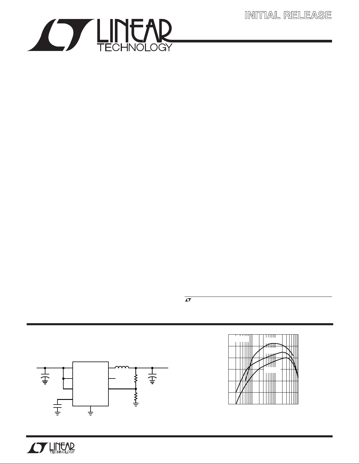
TYPICAL APPLICATIO
V
*
IN
3V TO
+
8.5V
22µF
16V
Figure 1a. High Efficiency Low Dropout Step-Down Converter
47pF
6
V
IN
2
RUN
7
SYNC/MODE
1
I
TH
LTC1707
GND
4
SW
V
REF
V
FB
U
15µH
5
8
3
*V
OUT
3V < VIN < 3.3V
+
249k
80.6k
FOLLOWS VIN FOR
100µF
6.3V
V
OUT
3.3V
1707 F01a
100
V
OUT
95
90
85
EFFICIENCY (%)
80
75
70
1
= 3.3V
10 100 1000
OUTPUT CURRENT (mA)
Figure 1b. Efficiency vs Output Load Current
Information furnished by Linear Technology Corporation is believed to be accurate and reliable.
However, no responsibility is assumed for its use. Linear Technology Corporation makes no representation that the interconnection of its circuits as described herein will not infringe on existing patent rights.
VIN = 3.6V
= 6V
V
IN
VIN = 8.4V
1707 F01b
1
LTC1707
WWWU
ABSOLUTE AXI U RATI GS
PACKAGE/ORDER I FOR ATIO
UU
W
(Note 1)
Input Supply Voltage ................................ –0.3V to 10V
I
Voltage ................................................. –0.3V to 5V
TH
RUN/SS, VFB Voltages ............................... – 0.3V to V
SYNC/MODE Voltage ................................. –0.3V to V
IN
IN
P-Channel Switch Source Current (DC) .............. 800mA
N-Channel Switch Sink Current (DC) .................. 800mA
Peak SW Sink and Source Current ......................... 1.5A
Operating Ambient Temperature Range
Commercial ............................................ 0°C to 70°C
I
RUN/SS
V
GND
TOP VIEW
1
TH
2
3
FB
4
S8 PACKAGE
8-LEAD PLASTIC SO
T
= 125°C, θJA = 110°C/ W
JMAX
8
V
SYNC/MODE
7
V
6
SW
5
REF
IN
ORDER PART
NUMBER
LTC1707CS8
LTC1707IS8
S8 PART MARKING
1707
1707I
Industrial ........................................... –40°C to 85°C
Junction Temperature (Note 2)............................. 125°C
Consult factory for Military grade parts.
Storage Temperature Range ................ –65°C to 150°C
Lead Temperature (Soldering, 10 sec)................. 300°C
ELECTRICAL CHARACTERISTICS
temperature range, otherwise specifications are at TA = 25°C. V
SYMBOL PARAMETER CONDITIONS MIN TYP MAX UNITS
I
VFB
V
FB
∆V
OVL
∆V
FB
V
LOADREG
I
S
V
RUN/SS
I
RUN/SS
I
SYNC/MODE
f
OSC
V
UVLO
R
PFET
R
NFET
I
PK
I
LSW
V
REF
∆V
REF
Note 1: Absolute Maximum Ratings are those values beyond which the life
of a device may be impaired.
Note 2: T
dissipation P
TJ = TA + (PD • 110°C/W)
Feedback Current (Note 3) 6 60 nA
Regulated Feedback Voltage (Note 3) ● 0.78 0.80 0.82 V
Output Overvoltage Lockout ∆V
Reference Voltage Line Regulation VIN = 3V to 8.5V (Note 3) 0.002 0.01 %/V
Output Voltage Load Regulation ITH Sinking 2µA (Note 3) 0.5 0.8 %
Input DC Bias Current (Note 4)
Pulse Skipping Mode VIN = 8.5V, V
Burst Mode Operation V
Shutdown V
Shutdown V
Run/SS Threshold V
Soft-Start Current Source V
SYNC/MODE Pull-Up Current V
Oscillator Frequency V
Undervoltage Lockout VIN Ramping Down from 3V (0°C to 70°C) 2.55 2.70 2.85 V
R
of P-Channel FET ISW = –100mA 0.5 0.7 Ω
DS(ON)
R
of N-Channel FET ISW = –100mA 0.6 0.8 Ω
DS(ON)
Peak Inductor Current VIN = 4V, ITH = 1.4V, Duty Cycle < 40% 0.70 0.915 1.10 A
SW Leakage V
Reference Output Voltage I
Reference Output Load Regulation 0V ≤ I
is calculated from the ambient temperature TA and power
J
according to the following formula:
D
I
TH
ITH
RUN/SS
RUN/SS
RUN/SS
RUN/SS
SYNC/MODE
FB
V
FB
V
IN
VIN Ramping Down from 3V (–40°C to 85°C) 2.45 2.70 2.85 V
V
IN
RUN/SS
REF
The ● denotes specifications which apply over the full operating
= 5V unless otherwise specified.
IN
= V
OVL
Sourcing 2µA (Note 3) –0.5 –0.8 %
= 0V, VIN = 8.5V, V
= 0.7V 315 350 385 kHz
= 0V 35 kHz
Ramping Up from 0V (0°C to 70°C) 2.60 2.80 3.00 V
Ramping Up from 0V (–40°C to 85°C) 2.50 2.80 3.00 V
= 0µA ● 1.178 1.19 1.202 mV
– V
OVL
FB
= 3.3V, V
OUT
= 0V, 3V < VIN < 8.5V 11 35 µA
= 0V, VIN < 3V 6 µA
Ramping Positive 0.4 0.7 1.0 V
= 0V 1.2 2.25 3.3 µA
= 0V 0.5 1.5 2.5 µA
= 0V ±10 ±1000 nA
≤ 100µA ● 2.3 15 mV
REF
SYNC/MODE
SYNC/MODE
Note 3: The LTC1707 is tested in a feedback loop that servos V
balance point for the error amplifier (V
Note 4: Dynamic supply current is higher due to the gate charge being
delivered at the switching frequency.
= 0V 300 µA
= Open 200 320 µA
20 60 110 mV
to the
= 0.8V).
ITH
FB
2
INPUT VOLTAGE (V)
2.5
4
SUPPLY CURRENT IN SHUTDOWN (µA)
6
10
12
14
6.5
22
1707 G06
8
4.5
3.5
7.5
5.5 8.5
16
18
20
V
RUN/SS
= 0V
T
J
= 85°C
TJ = 25°C
TJ = –40°C
UW
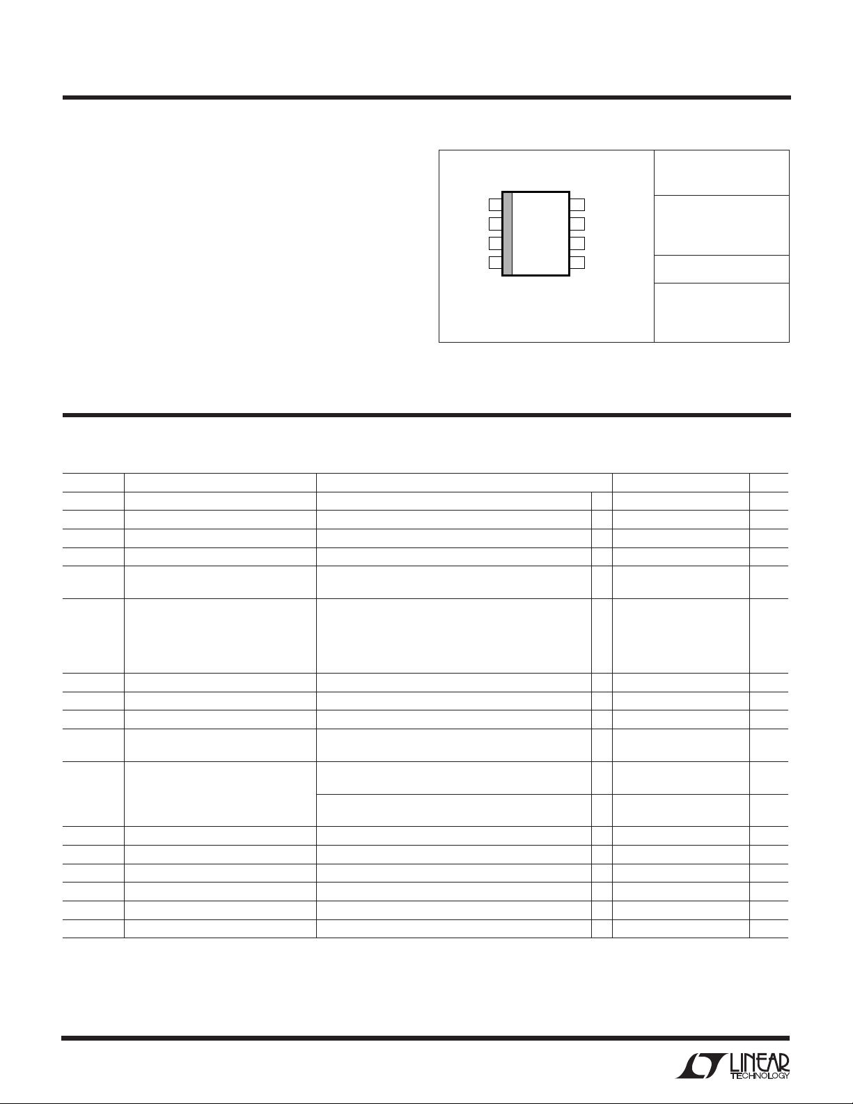
TYPICAL PERFOR A CE CHARACTERISTICS
LTC1707
Efficiency vs Input Voltage
100
95
90
85
EFFICIENCY (%)
80
V
OUT
L = 15µH
Burst Mode OPERATION
75
0
I
LOAD
= 2.5V
2
I
= 100mA
LOAD
I
LOAD
= 10mA
6
4
INPUT VOLTAGE (V)
Undervoltage Lockout Threshold
vs Temperature
3.00
2.95
2.90
2.85
2.80
2.75
2.70
2.65
2.60
2.55
UNDERVOLTAGE LOCKOUT THRESHOLD (V)
2.50
–50 –25
V
IN
RAMPING UP
V
IN
RAMPING DOWN
0 25 50 125
TEMPERATURE (°C)
75 100
= 300mA
8
1707 G04
1707 G01
10
Efficiency vs Load Current
100
95
Burst Mode
90
OPERATION
85
80
75
70
EFFICIENCY (%)
65
60
55
50
1
PULSE SKIPPING
MODE
10 100 1000
OUTPUT CURRENT (mA)
DC Supply Current
vs Input Voltage
350
300
250
200
150
100
DC SUPPLY CURRENT (µA)
TJ = 25°C
50
V
OUT
LOAD CURRENT = 0A
0
2.5
PULSE SKIPPING
= 1.8V
4.5
3.5
INPUT VOLTAGE (V)
MODE
Burst Mode
OPERATION
VIN = 3.6V
= 2.5V
V
OUT
L = 15µH
1707 G02
5.5 8.5
6.5
7.5
1707 G05
Efficiency vs Load Current
100
95
90
85
EFFICIENCY (%)
80
75
70
1
VIN = 7.2V
V
OUT
L = 15µH
Burst Mode OPERATION
10 100 1000
OUTPUT CURRENT (mA)
Supply Current in Shutdown
vs Input Voltage
VIN = 2.8V
VIN = 3.6V
= 2.5V
1707 G03
Reference Voltage
vs Temperature
1.200
VIN = 5V
1.195
1.190
1.185
REFERENCE VOLTAGE (V)
1.180
–50 –25
0 25 50 125
TEMPERATURE (°C)
75 100
1707 G07
Oscillator Frequency
vs Temperature
390
VIN = 5V
380
370
360
350
340
330
320
OSCILLATOR FREQUENCY (kHz)
310
300
–50 –25
0 25 50 125
TEMPERATURE (°C)
75 100
1707 G08
Oscillator Frequency
vs Input Voltage
390
380
370
360
350
340
330
320
OSCILLATOR FREQUENCY (kHz)
310
300
2.5
4.5
3.5
INPUT VOLTAGE (V)
5.5 8.5
6.5
7.5
1627 G09
3
LTC1707
UW
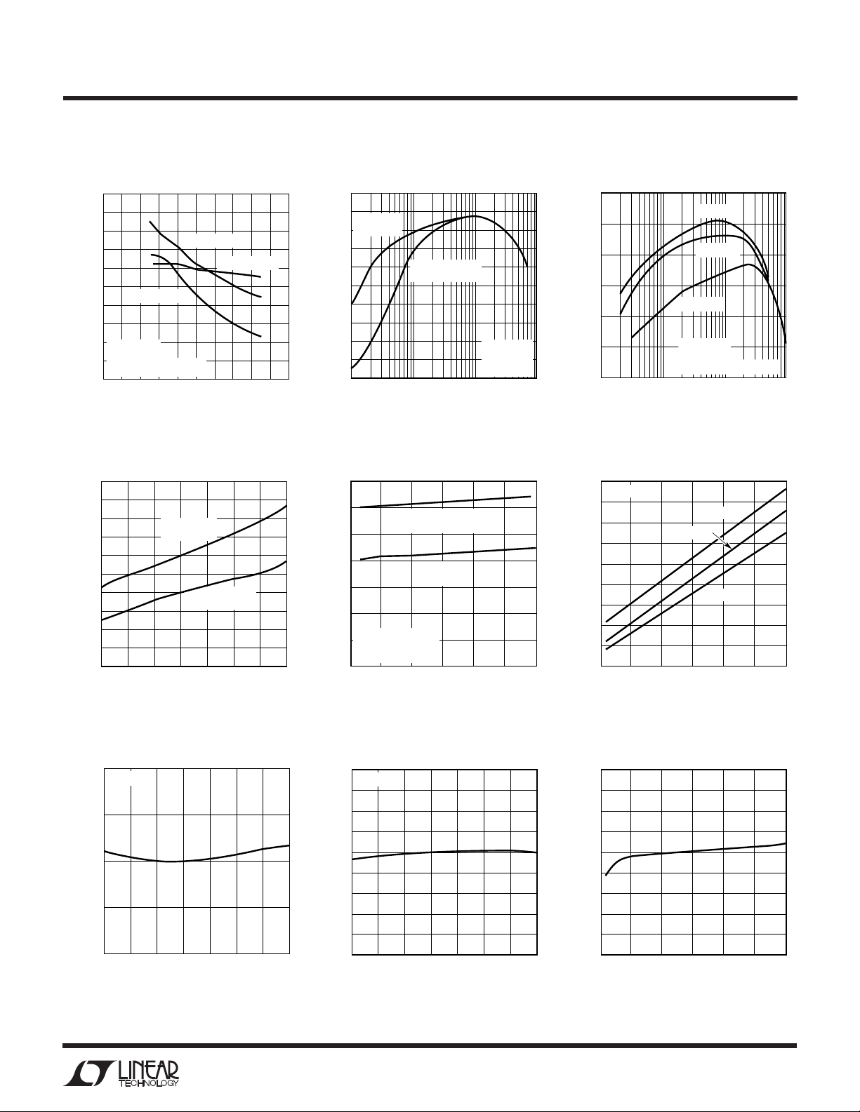
TYPICAL PERFOR A CE CHARACTERISTICS
Maximum Output Current vs
Input Voltage
1000
V
= 1.8V
800
600
400
OUTPUT CURRENT (mA)
200
OUT
= 1.5V
V
OUT
V
= 3.3V
V
OUT
V
= 2.5V
OUT
V
= 2.9V
OUT
0
2.5
4.5
3.5
INPUT VOLTAGE (V)
5.5 8.5
OUT
= 5V
6.5
TJ = 85°C
L = 15µH
7.5
1707 G10
Switch Leakage Current
vs Temperature
1800
VIN = 8.4V
1600
1400
1200
1000
800
600
SWITCH LEAKAGE (nA)
400
200
0
–50 –25
0 25 50 125
TEMPERATURE (°C)
SYNCHRONOUS
Switch Resistance
vs Input Voltage Load Step Transient Response
0.9
0.8
0.7
0.6
0.5
0.4
0.3
SWITCH RESISTANCE (Ω)
0.2
0.1
MAIN SWITCH
0
2.5
4.5
3.5
INPUT VOLTAGE (V)
SYNCHRONOUS SWITCH
5.5 8.5
6.5
7.5
1707 G13
I
0.5V/DIV
V
OUT
50mV/DIV
AC COUPLED
I
LOAD
500mA/DIV
TH
FIGURE 1A VIN = 5V FIGURE 1A I
25µs/DIV
SWITCH
SWITCH
75 100
MAIN
1707 G11
1707 G14
0.9
0.8
0.7
0.6
0.5
0.4
0.3
SWITCH RESISTANCE (Ω)
0.2
0.1
SW
5V/DIV
V
OUT
20mV/DIV
AC COUPLED
I
LOAD
200mA/DIV
Switch Resistance
vs Temperature
VIN = 5V
SYNCHRONOUS
SWITCH
0
–50 –25
0 25 50 125
TEMPERATURE (°C)
Burst Mode Operation
10µs/DIV
MAIN
SWITCH
75 100
VIN = 5V
= 50mA
LOAD
1707 G12
1707 G15
4
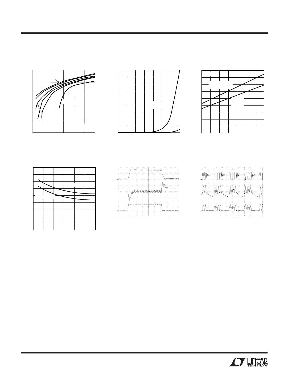
LTC1707
U
UU
PI FU CTIO S
I
(Pin 1): Error Amplifier Compensation Point. The
TH
current comparator threshold increases with this control
voltage. Nominal voltage range for this pin is 0V to 1.2V.
RUN/SS (Pin 2): Combination of Soft-Start and Run
Control Inputs. A capacitor to ground at this pin sets the
ramp time to full current output. The time is approximately
0.5s/µF. Forcing this pin below 0.4V shuts down the
LTC1707.
VFB (Pin 3): Feedback Pin. Receives the feedback voltage
from an external resistive divider across the output.
GND (Pin 4): Ground Pin.
SW (Pin 5): Switch Node Connection to Inductor. This pin
connects to the drains of the internal main and synchronous power MOSFET switches.
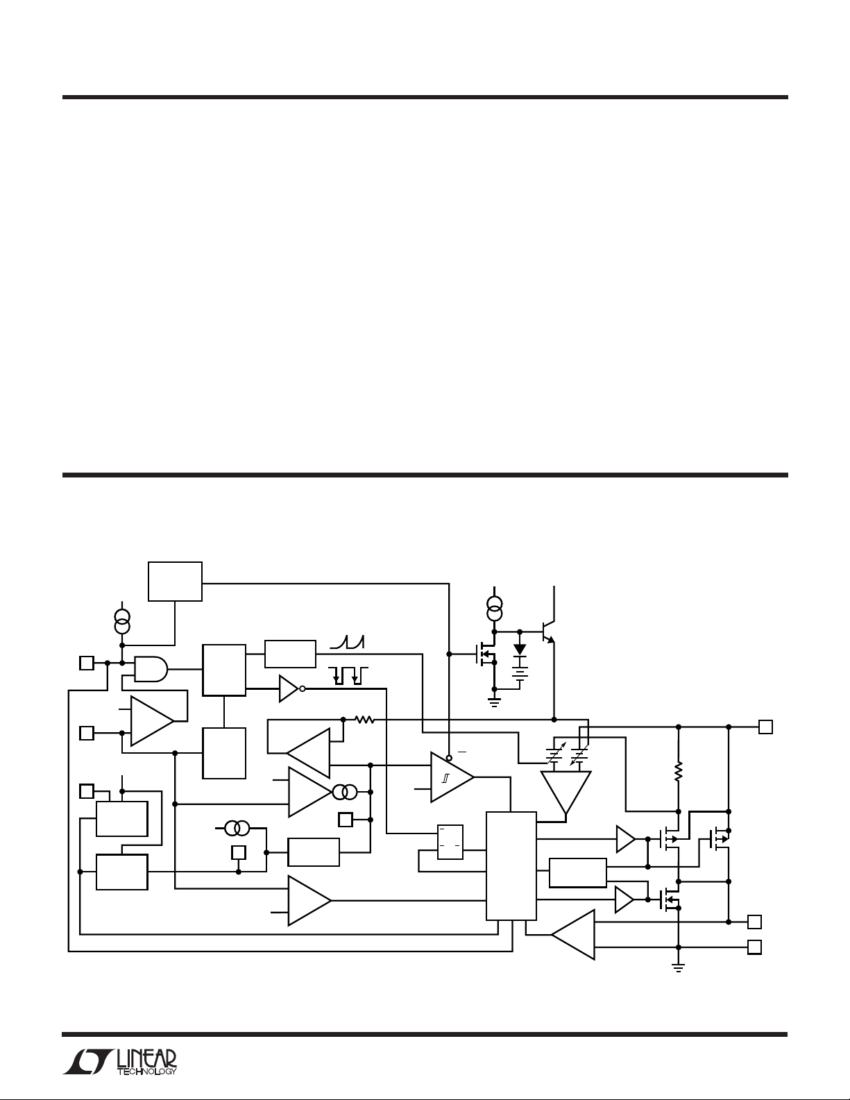
U
U
W
FU CTIO AL DIAGRA
VIN (Pin 6): Main Supply Pin. Must be closely decoupled
to GND, Pin 4.
SYNC/MODE (Pin 7):
This pin performs two functions:
1) synchronize with an external clock and 2) select between two modes of low load current operation. To
synchronize with an external clock, apply a TTL/CMOS
compatible clock with a frequency between 385kHz and
550kHz. To select Burst Mode operation, float the pin or
tie it to VIN. Grounding Pin 7 forces pulse skipping mode
operation.
V
(Pin 8): The Output of a 1.19V ±1% Precision
REF
Reference. May be loaded up to 100µA and is stable with
up to 2000pF load capacitance.
SYNC/MODE
7
V
FB
3
V
REF
8
SHUTDOWN
V
IN
1.5µA
0.6V
V
IN
1.19V
REF
UVLO
TRIP = 2.7V
BURST
DEFEAT
–
+
Y = “0” ONLY WHEN X IS A CONSTANT “1”
Y
X
SLOPE
OSC
FREQ
SHIFT
V
IN
RUN/SS
2.25µA
2
COMP
0.8V
0.86V
+
EA
–
RUN/SOFT
START
+
OVDET
–
V
IN
–
EN
+
0.12V
I
1
TH
–
+
BURST
SLEEP
QRS
SWITCHING
Q
LOGIC
AND
BLANKING
CIRCUIT
V
0.4V
IN
–
+
I
COMP
ANTI-
SHOOT-THRU
I
RCMP
6
V
IN
6Ω
+
–
SW
5
GND
4
1707 BD
5
 Loading...