

Linear Technology LTC1703 Datasheet
FEATURES
LTC1703
Dual 550kHz Synchronous
2-Phase Switching Regulator
Controller with 5-Bit VID
U
DESCRIPTIO
■
Two Independent PWM Controllers in One Package
■
Side 1 Output Is Compliant with Intel Mobile
VID Specifications (Includes 5-Bit DAC)
■
0.9V to 2.0V Output Voltage with 25mV/50mV Steps
■
Two Sides Run Out-of-Phase to Minimize C
■
All N-Channel External MOSFET Architecture
■
No External Current Sense Resistor
■
Precision Internal 0.8V ±1% Reference
■
550kHz Switching Frequency Minimizes External
IN
Component Size
■
Very Fast Transient Response
■
Up to 25A Output Current per Channel
■
Low Shutdown Current: < 100µA
■
Small 28-Pin SSOP Package
U
APPLICATIO S
■
Mobile Pentium® III Processor Systems
■
Microprocessor Core and I/O Supplies
■
Multiple Logic Supply Generator
■
High Efficiency Power Conversion
, LTC and LT are registered trademarks of Linear Technology Corporation.
Burst Mode is a trademark of Linear Technology Corporation. Pentium is a registered trademark
of Intel Corporation.
The LTC®1703 is a dual switching regulator controller optimized for high efficiency with low input voltages. It includes
two complete, on-chip, independent switching regulator
controllers. Each is designed to drive a pair of external
N-channel MOSFET devices in a voltage mode feedback,
synchronous buck configuration. The LTC1703 includes
digital output voltage adjustment on side 1 that conforms to
the Intel Mobile VID specification. It uses a constantfrequency, true PWM design switching at 550kHz, minimizing external component size and cost and optimizing load
transient performance. The synchronous buck architecture
automatically shifts to discontinuous and then to Burst
ModeTM operation as the output load decreases, ensuring
maximum efficiency over a wide range of load currents.
The LTC1703 features an onboard reference trimmed to 1%
and delivers better than 1.5% regulation at the converter
outputs. An optional latching FAULT mode protects the load
if the output rises 15% above the intended voltage. Each
channel can be enabled independently; with both channels
disabled, the LTC1703 shuts down and supply current drops
below 100µA.
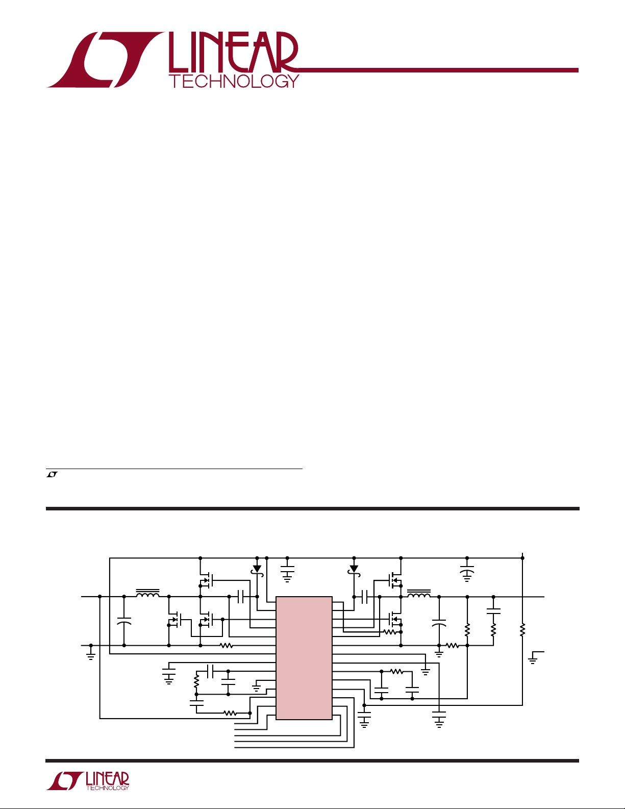
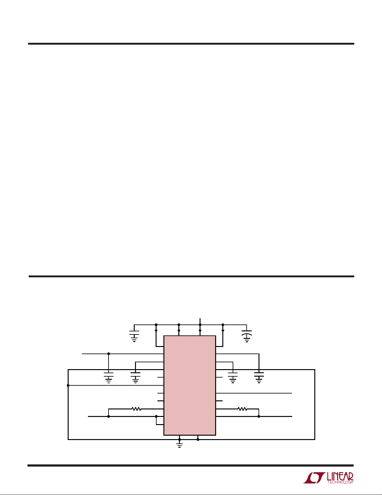
TYPICAL APPLICATIO
L1
V
OUT1
0.9V
TO 2V
15A
GND
L1: MURATA LQT12535C1R5N12
L2: COILTRONICS UP2B-2R2
QT1, QB1A, QB1B: INTERNATIONAL RECTIFIER IRF7811
QT2, QB2: 1/2 FAIRCHILD NDS8926
1µH
C
OUT1
+
180µF
4V
× 6
C
SS1
0.22µF
QB1A
220pF
100k
C31
QT1
R21
U
Dual Output Mobile Pentium III Processor Supply
MBR0520LT1
I
MAX2
BOOST2
BG2
TG2
SW2
PGND
FAULT
RUN/SS2
COMP2
FB2
V
CC
VID4
VID3
VID2
DCP2
28
27
26
25
24
23
22
21
20
19
18
17
16
15
CCP2
1µF
QT2
R22, 100k
1µF
QB1B
C11
220pF
DCP1
MBR0520LT1
CCP1
1µF
R
IMAX1
C21
15pF
R31, 10k
VID0
VID1
VID2
VID3
VID4
,18.7k
1
2
3
4
5
6
7
8
9
10
11
12
13
14
PV
CC
BOOST1
BG1
TG1
SW1
I
MAX1
FCB
RUN/SS1
COMP1
SGND
FB1
SENSE
VID0
VID1
1µF
LTC1703
C22
15pF
QB2
R
20k
2.2µH
IMAX2
L2
C12
220pF
V
IN
4.5V TO 5.5V
+
C
IN
150µF
10V
× 2
C32
+
C
OUT2
180µF
4V
RB2
11.5k
0.1%
C
SS2
0.22µF
R12
10.2k
0.1%
2200pF
R32
1k
10Ω
GND
1703 TA01
V
1.5V
3A
GND
OUT2
1
LTC1703
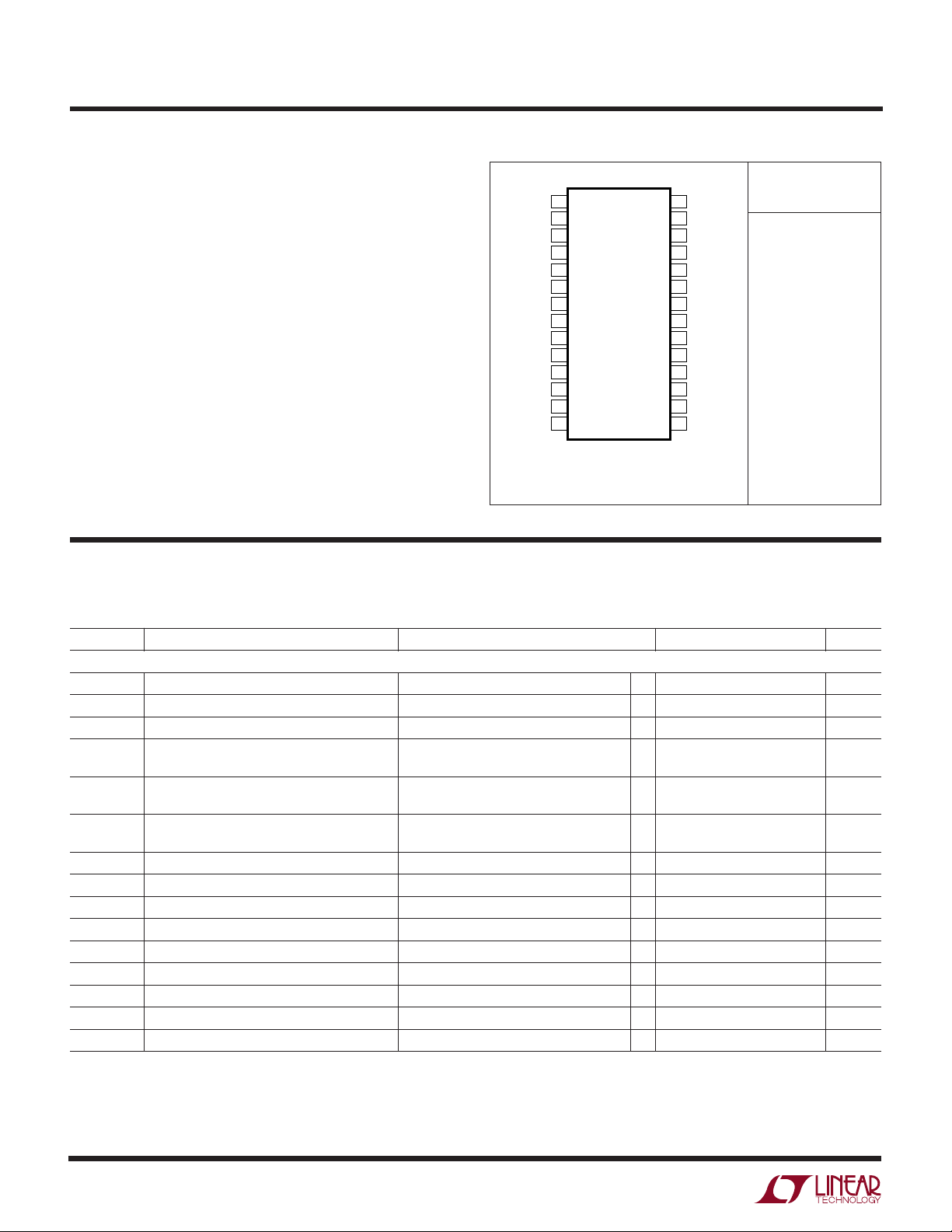
PACKAGE/ORDER I FOR ATIO
UU
W
WWWU
ABSOLUTE AXI U RATI GS
(Note 1)
Supply Voltage
V
...........................................................................................
CC
BOOST
n...............................................................
BOOSTn – SWn.................................................... 7V
Input Voltage
SWn.......................................................... –1V to 8V
VIDn....................................................... –0.3V to 7V
All Other Inputs ......................... – 0.3V to VCC + 0.3V
Peak Output Current < 10µs
TGn, BGn............................................................... 5A
Operating Temperature Range .................... 0°C to 85°C
Storage Temperature Range ................. –65°C to 150°C
Lead Temperature (Soldering, 10 sec).................. 300°C
7V
15V
PV
BOOST1
BG1
TG1
SW1
I
MAX1
FCB
RUN/SS1
COMP1
SGND
FB1
SENSE
VID0
VID1
TOP VIEW
1
CC
2
3
4
5
6
7
8
9
10
11
12
13
14
G PACKAGE
28-LEAD PLASTIC SSOP
T
= 125°C, θJA = 55°C/W
JMAX
28
27
26
25
24
23
22
21
20
19
18
17
16
15
I
MAX2
BOOST2
BG2
TG2
SW2
PGND
FAULT
RUN/SS2
COMP2
FB2
V
CC
VID4
VID3
VID2
ORDER PART
LTC1703CG
Consult factory for Industrial and Military grade parts.
NUMBER
ELECTRICAL CHARACTERISTICS
The ● denotes specifications which apply over the full operating temperature range, otherwise specifications are TA = 25°C.
VCC = 5V unless otherwise specified. (Note 3)
SYMBOL PARAMETER CONDITIONS MIN TYP MAX UNITS
Main Control Loop
V
CC
PV
CC
BV
CC
I
CC
IPV
I
BOOST
V
FB
∆V
FB
I
FB
∆V
OUT
V
FCB
∆V
FCB
I
FCB
V
RUN
I
SS
CC
VCC Supply Voltage ● 37V
PVCC Supply Voltage (Note 2) ● 37V
BOOST Pin Voltage V
– VSW (Note 2) ● 2.7 7 V
BOOST
VCC Supply Current Test Circuit 1 ● 2.2 8 mA
RUN/SS1 = RUN/SS2 = 0V (Note 5)
● 30 100 µA
PVCC Supply Current Test Circuit 1 (Note 4) ● 2.2 6 mA
RUN/SS1 = RUN/SS2 = 0V (Note 5)
● 6 100 µA
BOOST Pin Current Test Circuit 1 (Note 4) ● 1.3 3 mA
RUN/SS1 = RUN/SS2 = 0V
● 0.1 10 µA
Feedback Voltage Test Circuit 1 ● 0.792 0.800 0.808 V
Feedback Voltage Line Regulation VCC = 3V to 7V ● ±0.005 ±0.05 %/V
Feedback Current FB2 Only (Note 8) ● ±0.001 ±1 µA
Output Voltage Load Regulation (Note 6) ● 0.1 ±0.2 %
FCB Threshold ● 0.75 0.8 0.85 V
FCB Feedback Hysteresis 20 mV
FCB Pin Current ● ±0.001 ±1 µA
RUN/SS Pin RUN Threshold ● 0.45 0.55 0.65 V
Soft Start Source Current RUN/SSn = 0V –1.5 –3.5 –5.5 µA
2
LTC1703
ELECTRICAL CHARACTERISTICS
The ● denotes specifications which apply over the full operating temperature range, otherwise specifications are TA = 25°C.
VCC = 5V unless otherwise specified. (Note 3)
SYMBOL PARAMETER CONDITIONS MIN TYP MAX UNITS
Switching Characteristics
V
OSC
f
OSC
Φ
OSC2
DC
MIN1
DC
MIN2
DC
MAX
t
NOV
tr, t
f
Feedback Amplifier
A
VFB
GBW FB Gain Bandwidth 25 MHz
I
ERR
V
MIN
V
MAX
Current Limit Loop
A
VILIM
I
IMAX
Status Outputs
V
FAULT
V
OLF
I
FAULT
t
FAULT
VID Inputs
R11 Resistance Between SENSE and FB1 10 kΩ
V
Error % Output Voltage Accuracy (Side 1) Programmed from 0.9V to 2V ● –1.5 1.5 %
OUT
R
PULLUP
VID
T
I
VID-LEAK
V
PULLUP
Oscillator Amplitude 1V
P-P
Oscillator Frequency Test Circuit 1 ● 475 550 750 kHz
Controller 2 Oscillator Phase Relative to Controller 1 180 DEG
Minimum Duty Cycle VFB < V
Minimum Duty Cycle VFB > V
MAX
MAX
● 710 %
● 0%
Maximum Duty Cycle ● 87 90 93 %
Driver Nonoverlap Test Circuit 1 (Note 9) ● 40 100 ns
Driver Rise/Fall Time Test Circuit 1 (Note 9) ● 12 80 ns
FB DC Gain ● 74 85 dB
FB Sink/Source Current COMPN Output ● ±3 ±10 mA
MIN Comparator Threshold ● 760 785 mV
MAX Comparator Threshold ● 815 840 mV
I
Gain 40 dB
LIM
I
Source Current I
MAX
FAULT Trip Point VFB Relative to Regulated V
FAULT Output Low Voltage I
FAULT Output Current V
FAULT Delay Time VFB > V
VID Input Pull-Up Resistance V
= 0V ● –7 –10 –13 µA
MAX
OUT
= 1mA ● 0.03 0.1 V
FAULT
= 0V –10 µA
FAULT
to FAULT (Note 9) 25 µs
FAULT
= 0.6V (Note 7) 40 kΩ
DIODE
● +10 +15 +20 %
VID Input Voltage Threshold VIL (2.7V ≤ VCC ≤ 5.5V) 0.4 V
VIH (2.7V ≤ VCC ≤ 5.5V) 1.6 V
VID Input Leakage Current VCC < VID < 7V (Note 7) 0.01 ±1 µA
VID Pull-Up Voltage VCC = 3.3V 2.8 V
VCC = 5V 4.5 V
Note 1: Absolute Maximum Ratings are those values beyond which the life
of a device may be impaired.
Note 2: PV
and BVCC (V
CC
– VSW) must be greater than V
BOOST
GS(ON)
of
the external MOSFETs used to ensure proper operation.
Note 3: All currents into device pins are positive; all currents out of device
pins are negative. All voltages are referenced to ground unless otherwise
specified.
Note 4: Supply current in normal operation is dominated by the current
needed to charge and discharge the external MOSFET gates. This current
will vary with supply voltage and the external MOSFETs used.
Note 5: Supply current in shutdown is dominated by external MOSFET
leakage and may be significantly higher than the quiescent current drawn
by the LTC1703, especially at elevated temperature.
Note 6: This parameter is guaranteed by correlation and is not tested
directly.
Note 7: Each built-in pull-up resistor attached to the VID inputs also has a
series diode connected to V
to allow input voltages higher than the V
CC
CC
supply without damage or clamping. (See Block Diagram.)
Note 8: Feedback current at FB1 will be higher due to internal VID
resistors.
Note 9: Rise and fall times are measured using 10% and 90% levels. Delay
and nonoverlap times are measured using 50% levels.
3
LTC1703
TEMPERATURE (°C)
–50
0.4
R
ON
(Ω)
0.5
0.7
0.8
0.9
1.4
1.1
0
50
75
1703 G06
0.6
1.2
1.3
1.0
–25
25
100
125
V
PVCC
= 5V
V
BOOST
– VSW = 5V
GATE CAPACITANCE (pF)
0
25
30
35
6000 8000
1703 G03
20
15
2000 4000 10000
10
5
0
DRIVER SUPPLY CURRENT (mA)
TEST CIRCUIT 1
ONE DRIVER LOADED
MULTIPLY BY # OF ACTIVE
DRIVERS TO OBTAIN TOTAL
DRIVER SUPPLY CURRENT
TEMPERATURE (°C)
–50 –25
12
RISE/FALL TIME (ns)
12
15
0
50
75
1703 G09
11
14
13
25
100
125
TEST CIRCUIT 1
C
L
= 2000pF
UW
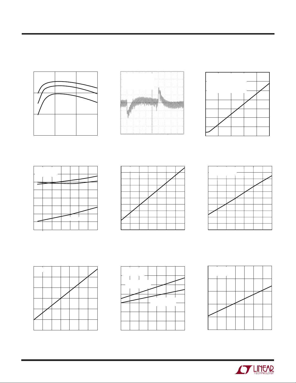
TYPICAL PERFOR A CE CHARACTERISTICS
Efficiency vs Load Current
100
= 5V
V
IN
90
EFFICIENCY (%)
80
V
OUT
V
OUT
V
OUT
= 3.3V
= 2.5V
= 1.6V
Transient Response
VIN = 5V
= 1.8V
V
OUT
I
= 0A-10A-0A
LOAD
±2.2% MAX DEVIATION
20mV/
DIV
MOSFET Driver Supply Current
vs Gate Capacitance
70
0
Supply Current vs Temperature
2.6
TEST CIRCUIT 1
= 0pF
C
2.4
L
2.2
2.0
1.8
1.6
SUPPLY CURRENT (mA)
1.4
1.2
1.0
–25 0 50
–50
RUN/SS Source Current
vs Temperature
5.0
VCC = 5V
4.5
4.0
3.5
3.0
SOURCE CURRENT (µA)
2.5
2.0
–50
–25 0
4
510
LOAD CURRENT (A)
PV
CC
V
CC
BOOST1, BOOST2
25
TEMPERATURE (°C)
50 100 125
25 75
TEMPERATURE (°C)
15
1703 G01
75 100 125
1703 G04
1703 G07
10µs/DIV
1703 G02
Normalized Frequency
vs Temperature Driver RON vs Temperature
2.5
VCC = 5V
2.0
1.5
1.0
0.5
0
–0.5
–1.0
–1.5
NORMALIZED FREQUENCY (%)
–2.0
–2.5
–50
0
–25
TEMPERATURE (°C)
50
25
75
100
125
1703 G05
Nonoverlap Time vs Temperature Driver Rise/Fall vs Temperature
70
TEST CIRCUIT 1
C
= 2000pF
L
60
TG FALLING EDGE
50
BG RISING EDGE
40
30
NONOVERLAP (ns)
20
10
0
–50
–25 0
BG FALLING EDGE
TG RISING EDGE
50 100 125
25 75
TEMPERATURE (°C)
1703 G08

LTC1703
U
UU
PI FU CTIO S
PVCC (Pin 1): Driver Power Supply Input. PVCC provides
power to the two BGn output drivers. PVCC must be
connected to a voltage high enough to fully turn on the
external MOSFETs QB1 and QB2. PVCC should generally
be connected directly to VIN. PVCC requires at least a 1µF
bypass capacitor directly to PGND.
BOOST1 (Pin 2): Controller 1 Top Gate Driver Supply. The
BOOST1 pin supplies power to the floating TG1 driver.
BOOST1 should be bypassed to SW1 with a 1µF capacitor.
An additional Schottky diode from VIN to BOOST1 pin will
create a complete floating charge-pumped supply at
BOOST1. No other external supplies are required.
BG1 (Pin 3): Controller 1 Bottom Gate Drive. The BG1 pin
drives the gate of the bottom N-channel synchronous
switch MOSFET, QB1. BG1 is designed to drive up to
10,000pF of gate capacitance directly. If RUN/SS1 goes
low, BG1 will go low, turning off QB1. If FAULT mode is
tripped, BG1 will go high and stay high, keeping QB1 on
until the power is cycled.
TG1 (Pin 4): Controller 1 Top Gate Drive. The TG1 pin
drives the gate of the top N-channel MOSFET, QT1. The
TG1 driver draws power from the BOOST1 pin and returns
to the SW1 pin, providing true floating drive to QT1. TG1
is designed to drive up to 10,000pF of gate capacitance
directly. In shutdown or fault modes, TG1 will go low.
SW1 (Pin 5): Controller 1 Switching Node. SW1 should be
connected to the switching node of converter 1. The TG1
driver ground returns to SW1, providing floating gate
drive to the top N-channel MOSFET switch, QT1. The
voltage at SW1 is compared to I
comparator while the bottom MOSFET, QB1, is on.
I
(Pin 6): Controller 1 Current Limit Set. The I
MAX1
pin sets the current limit comparator threshold for
controller 1. If the voltage drop across the bottom MOSFET,
QB1, exceeds the magnitude of the voltage at I
controller 1 will go into current limit. The I
internal 10µA current source pull-up, allowing the current
threshold to be set with a single external resistor to PGND.
This current setting resistor should be Kelvin connected to
the source of QB1. See the Current Limit Programming
section for more information on choosing R
by the current limit
MAX1
MAX1
IMAX
MAX1
MAX1
pin has an
.
,
FCB (Pin 7): Force Continuous Bar. The FCB pin forces
both converters to maintain continuous synchronous
operation regardless of load when the voltage at FCB
drops below 0.8V. FCB is normally tied to VCC. To force
continuous operation, tie FCB to SGND. FCB can also be
connected to a feedback resistor divider from a secondary
winding on one converter’s inductor to generate a third
regulated output voltage. Do not leave FCB floating.
RUN/SS1 (Pin 8): Controller 1 Run/Soft-Start. Pulling
RUN/SS1 to SGND will disable controller 1 and turn off
both of its external MOSFET switches. Pulling both
RUN/SS pins down will shut down the entire LTC1703,
dropping the quiescent supply current below 100µA. A
capacitor from RUN/SS1 to SGND will control the turn-on
time and rate of rise of the controller 1 output voltage at
power-up. An internal 3.5µA current source pull-up at
RUN/SS1 pin sets the turn-on time at approximately
50ms/µF.
COMP1 (Pin 9): Controller 1 Loop Compensation. The
COMP1 pin is connected directly to the output of the first
controller’s error amplifier and the input to the PWM
comparator. An RC network is used at the COMP1 pin to
compensate the feedback loop for optimum transient
response.
SGND (Pin 10): Signal Ground. All internal low power
circuitry returns to the SGND pin. Connect to a low
impedance ground, separated from the PGND node. All
feedback, compensation and soft-start connections should
return to SGND. SGND and PGND should connect only at
a single point, near the PGND pin and the negative plate of
the CIN bypass capacitor.
FB1 (Pin 11): Controller 1 Feedback Input. The loop
compensation network for controller 1 should be connected to FB1. FB1 is connected internally to the VID
resistor network to set the output voltage at side 1.
SENSE (Pin 12): Output Sense. Connect to V
VID0 to VID4 (Pins 13 to 17): VID Programming Inputs.
These are logic inputs that set the output voltage at side 1
to a preprogrammed value (see Table 1). VID4 is the MSB,
VID0 is the LSB. The codes selected by the VIDn inputs
correspond to the Intel Mobile VID specification. Each
OUT1
.
5
LTC1703
U
UU
PI FU CTIO S
VIDn pin includes an on-chip 40kΩ pull-up resistor in
series with a diode (see Block Diagram).
VCC (Pin 18): Power Supply Input. All internal circuits
except the output drivers are powered from this pin. V
should be connected to a low noise power supply voltage
between 3V and 7V and should be bypassed to SGND with
at least a 1µF capacitor in close proximity to the LTC1703.
FB2 (Pin 19): Controller 2 Feedback Input. FB2 should be
connected through a resistor divider network to V
set the ouput voltage. The loop compensation network for
controller 2 also connects to FB2.
COMP2 (Pin 20): Controller 2 Loop Compensation. See
COMP1.
RUN/SS2 (Pin 21): Controller 2 Run/Soft-Start. See RUN/
SS1.
FAULT (Pin 22): Output Overvoltage Fault (Latched). The
FAULT pin is an open-drain output with an internal 10µA
pull-up. If either regulated output voltage rises more than
15% above its programmed value for more than 25µs, the
FAULT output will go high and the entire LTC1703 will be
OUT2
CC
to
disabled. When FAULT is high, both BG pins will go high,
turning on the bottom MOSFET switches and pulling down
the high output voltage. The LTC1703 will remain latched
in this state until the power is cycled. When FAULT mode
is active, the FAULT pin will be pulled up with an internal
10µA current source. Tying FAULT directly to SGND will
disable latched FAULT mode and will allow the LTC1703 to
resume normal operation when the overvoltage fault is
removed.
PGND (Pin 23): Power Ground. The BGn drivers return to
this pin. Connect PGND to a high current ground node in
close proximity to the sources of external MOSFETs, QB1
and QB2, and the VIN and V
bypass capacitors.
OUT
SW2 (Pin 24): Controller 2 Switching Node. See SW1.
TG2 (Pin 25): Controller 2 Top Gate Drive. See TG1.
BG2 (Pin 26): Controller 2 Bottom Gate Drive. See BG1.
BOOST2 (Pin 27): Controller 2 Top Gate Driver Supply.
See BOOST1.
I
(Pin 28): Controller 2 Current Limit Set. See I
MAX2
MAX1
.
TEST CIRCUIT
f
OSC
MEASURED
V
FB1
Test Circuit 1
5V
I
0.1µF
2000pF 2000pF
2k
BOOST1ICC
V
CC
BOOST1
TG1
BG1
2000pF
SW1
I
MAX1
LTC1703
FCB
VID0:4
NC
RUN/SS1
NC NC
COMP1
FB1
SENSE
GND PGND
I
PVCC
PV
CC
BOOST2
SW2
I
MAX2
FAULT
RUN/SS2
COMP2
TG2
BG2
FB2
I
BOOST2
+
2000pF
2k
100µF
V
V
FAULT
FB2
1703 TC
6
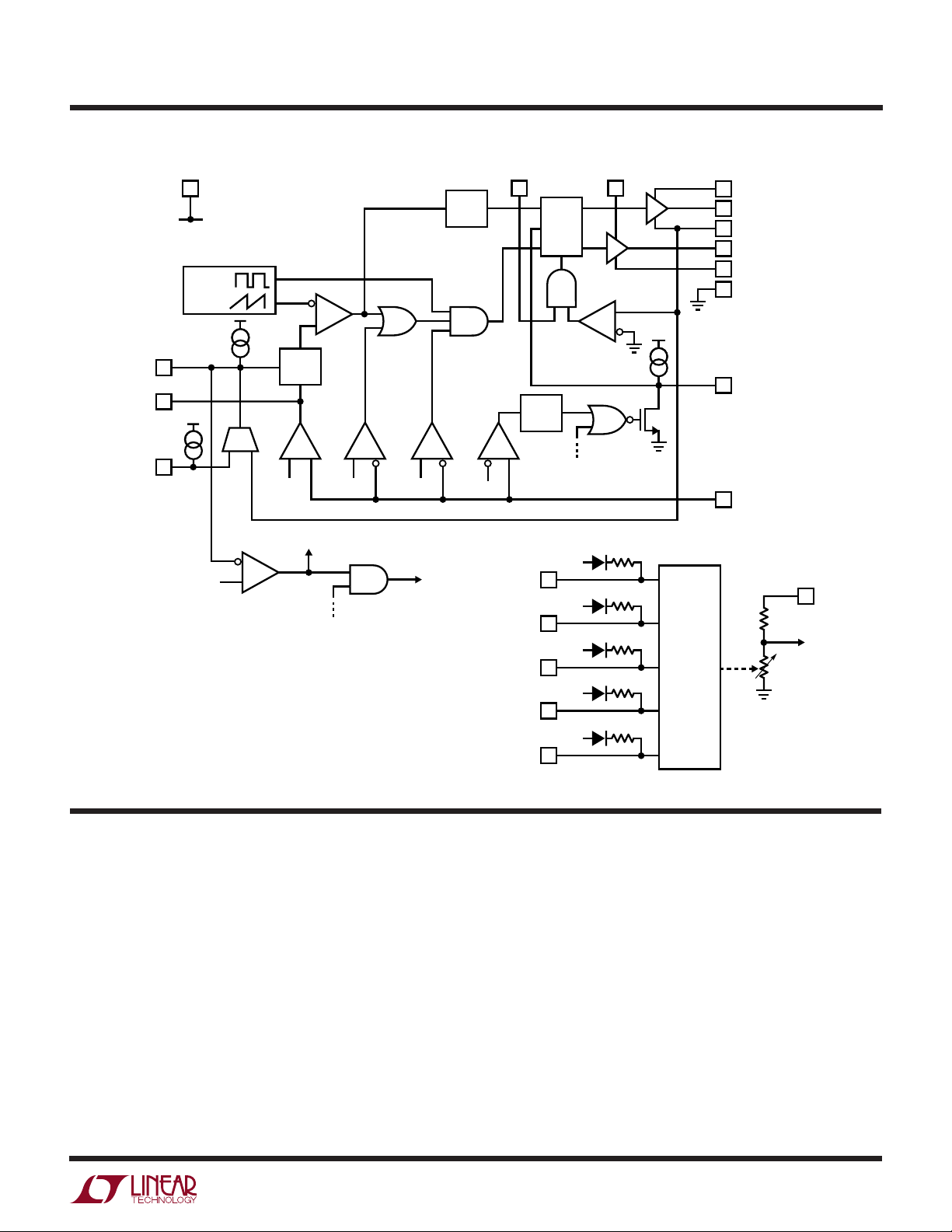
BLOCK DIAGRA
V
CC
OSC
550kHz
4µA
RUN/SS1,2
COMP1,2
I
LIM
I
MAX1,2
10µA
500mV
W
90% DUTY CYCLE
SOFT
START
FB
+
–
800mV 760mV 840mV
SHUTDOWN TO
THIS CONTROLLER
CONTROLLER
MIN MAX
FROM
OTHER
BURST
LOGIC
920mV
SHUTDOWN TO
ENTIRE CHIP
FLT
0V
FCB
VID0
VID1
VID2
VID3
VID4
DRIVE
LOGIC
25µs
DELAY
CONTROLLER
FROM
OTHER
V
CC
V
CC
V
CC
V
CC
V
CC
DIS
LTC1703
PV
CC
40k
40k
40k
40k
40k
10µA
SWITCH
CONTROL
LOGIC
BOOST1,2
TG1,2
SW1,2
BG1,2
PGND
SGND
FAULT
FB1,2
R11
10k
R
SENSE
TO FB1
B1
1703 BD
WUUU
APPLICATIO S I FOR ATIO
OVERVIEW
The LTC1703 is a dual, step-down (buck), voltage mode
feedback switching regulator controller. It is designed to
be used in a synchronous switching architecture with two
external N-channel MOSFETs per channel. It is intended to
operate from a low voltage input supply (7V maximum)
and provide a high power, high efficiency, precisely regulated output voltage. Several features make it particularly
suited for microprocessor supply regulation. Output regulation is extremely tight, with DC line and load regulation
and initial accuracy better than 1.5%, and total regulation
including transient response inside of 3.5% with a prop-
erly designed circuit. The 550kHz switching frequency
allows the use of physically small, low value external
components without compromising performance. An
onboard DAC sets the output voltage at channel 1, consistent with the Intel mobile VID specification (Table 1).
The LTC1703’s internal feedback amplifier is a 25MHz
gain-bandwidth op amp, allowing the use of complex
multipole/zero compensation networks. This allows the
feedback loop to maintain acceptable phase margin at
higher frequencies than traditional switching regulator
controllers allow, improving stability and maximizing transient response. The 800mV internal reference allows
7
LTC1703
WUUU
APPLICATIO S I FOR ATIO
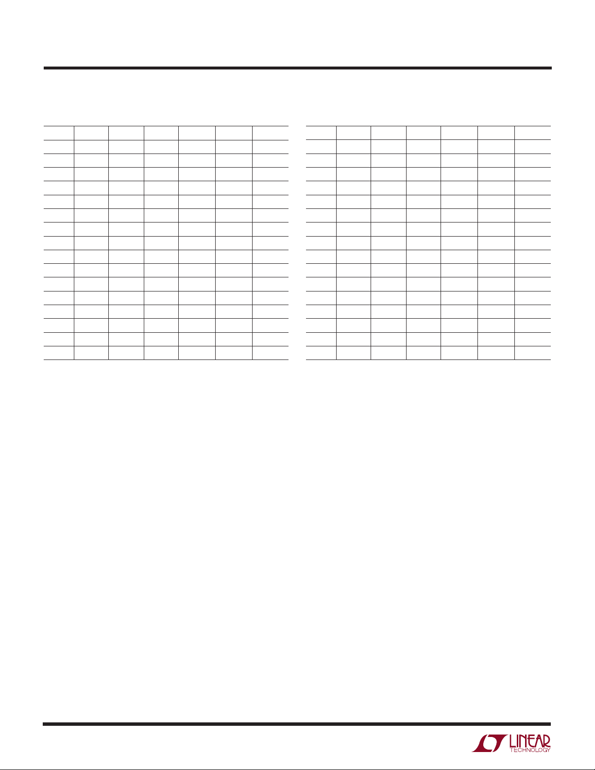
Table 1. VID Inputs and Corresponding Output Voltage for
Channel 1
CODE VID4 VID3 VID2 VID1 VID0 V
00000 GND GND GND GND GND 2.00V
00001 GND GND GND GND Float 1.95V
00010 GND GND GND Float GND 1.90V
00011 GND GND GND Float Float 1.85V
00100 GND GND Float GND GND 1.80V
00101 GND GND Float GND Float 1.75V
00110 GND GND Float Float GND 1.70V
00111 GND GND Float Float Float 1.65V
01000 GND Float GND GND GND 1.60V
01001 GND Float GND GND Float 1.55V
01010 GND Float GND Float GND 1.50V
01011 GND Float GND Float Float 1.45V
01100 GND Float Float GND GND 1.40V
01101 GND Float Float GND Float 1.35V
01110 GND Float Float Float GND 1.30V
01111* GND Float Float Float Float 1.25V
* 01111 and 11111 are defined by Intel to signify “no CPU.” The LTC1703
will generate the output voltages shown when these codes are selected.
OUT1
CODE VID4 VID3 VID2 VID1 VID0 V
10000 Float GND GND GND GND 1.275V
10001 Float GND GND GND Float 1.250V
10010 Float GND GND Float GND 1.225V
10011 Float GND GND Float Float 1.200V
10100 Float GND Float GND GND 1.175V
10101 Float GND Float GND Float 1.150V
10110 Float GND Float Float GND 1.125V
10111 Float GND Float Float Float 1.100V
11000 Float Float GND GND GND 1.075V
11001 Float Float GND GND Float 1.050V
11010 Float Float GND Float GND 1.025V
11011 Float Float GND Float Float 1.000V
11100 Float Float Float GND GND 0.975V
11101 Float Float Float GND Float 0.950V
11110 Float Float Float Float GND 0.925V
11111* Float Float Float Float Float 0.900V
OUT1
regulated output voltages as low as 800mV without external level shifting amplifiers.
The LTC1703’s synchronous switching logic transitions
automatically into Burst Mode operation, maximizing efficiency with light loads. An onboard overvoltage (OV) fault
flag indicates when an OV fault has occurred. The OV flag
can be set to latch the device off when an OV fault has
occurred, or to automatically resume operation when the
fault is removed.
2-Step Conversion
“2-step” architectures use a primary regulator to convert
the input power source (batteries or AC line voltage) to an
intermediate supply voltage, often 5V. This intermediate
voltage is then converted to the low voltage, high current
supplies required by the system using a secondary regulator—the LTC1703. 2-step conversion eliminates the
need for a single converter that converts a high input
voltage to a very low output voltage, often an awkward
design challenge. It also fits naturally into systems that
continue to use the 5V supply to power portions of their
circuitry, or have excess 5V capacity available as newer
circuit designs shift the current load to lower voltage
supplies.
Each regulator in a typical 2-step system maintains a
relatively low step-down ratio (5:1 or less), running at high
efficiency while maintaining a reasonable duty cycle. In
contrast, a regulator taking a single step from a high input
voltage to a 1.xV output must run at a very narrow duty
cycle, mandating trade-offs in external component values
while compromising efficiency and transient response.
The efficiency loss can exceed that of using a 2-step
solution (see the 2-Step Efficiency Calculation section and
Figure 10). Further complicating the calculation is the fact
that many systems draw a significant fraction of their total
power off the intermediate 5V supply, bypassing the low
voltage supply. 2-step solutions using the LTC1703 usually match or exceed the total system efficiency of singlestep solutions, and provide the additional benefits of
improved transient response, reduced PCB area and simplified power trace routing.
2-step regulation can buy advantages in thermal management as well. Power dissipation in the LTC1703 portion of
a 2-step circuit is lower than it would be in a typical 1-step
8

WUUU
APPLICATIO S I FOR ATIO
LTC1703
converter, even in cases where the 1-step converter has
higher total efficiency than the 2-step system. In a typical
microprocessor core supply regulator, for example, the
regulator is usually located right next to the CPU. In a
1-step design, all of the power dissipated by the core
regulator is right there next to the hot CPU, aggravating
thermal management. In a 2-step LTC1703 design, a
significant percentage of the power lost in the core regulation system happens in the 5V supply, which is usually
located away from the CPU. The power lost to heat in the
LTC1703 section of the system is relatively low, minimizing the added heat near the CPU.
See the Optimizing Performance section for a detailed
explanation of how to calculate system efficiency.
2-Phase Operation
The LTC1703 dual switching regulator controller also
features the considerable benefits of 2-phase operation.
Notebook computers, handheld terminals and automotive
electronics all benefit from the lower input filtering
requirement, reduced electromagnetic interference (EMI)
and increased efficiency associated with 2-phase
operation.
Why the need for 2-phase operation? Up until the LTC1703,
constant-frequency dual switching regulators operated
both channels in phase (i.e., single-phase operation). This
means that both topside MOSFETs turned on at the same
time, causing current pulses of up to twice the amplitude
of those for one regulator to be drawn from the input
capacitor. These large amplitude current pulses increased
the total RMS current flowing from the input capacitor,
requiring the use of more expensive input capacitors and
increasing both EMI and losses in the input capacitor and
input power supply.
With 2-phase operation, the two channels of the LTC1703
are operated 180 degrees out of phase. This effectively
interleaves the current pulses coming from the switches,
greatly reducing the overlap time where they add together.
The result is a significant reduction in total RMS input
current, which in turn allows less expensive input capacitors to be used, reduces shielding requirements for EMI
and improves real world operating efficiency.
Figure 7 shows example waveforms for a single switching
regulator channel versus a 2-phase LTC1703 system with
both sides switching. A single-phase dual regulator with
both sides operating would exhibit double the single side
numbers. In this example, 2-phase operation reduced the
RMS input current from 9.3A
4.8A
remember that the power losses are proportional to I
meaning that the actual power wasted is reduced by a
factor of 3.75. The reduced input ripple voltage also means
less power is lost in the input power path, which could
include batteries, switches, trace/connector resistances
and protection circuitry. Improvements in both conducted
and radiated EMI also directly accrue as a result of the
reduced RMS input current and voltage.
Small Footprint
The LTC1703 operates at a 550kHz switching frequency,
allowing it to use low value inductors without generating
excessive ripple currents. Because the inductor stores
less energy per cycle, the physical size of the inductor can
be reduced without risking core saturation, saving PCB
board space. The high operating frequency also means
less energy is stored in the output capacitors between
cycles, minimizing their required value and size. The
remaining components, including the SSOP-28 LTC1703,
are tiny, allowing an entire dual-output LTC1703 circuit to
be constructed in 1.5in2 of PCB space. Further, this space
is generally located right next to the microprocessor or in
some similarly congested area, where PCB real estate is at
a premium. The fact that the LTC1703 runs off the 5V
supply, often available from a power plane, is an added
benefit in portable systems —it does not require a dedicated supply line running from the battery.
Fast Transient Response
The LTC1703 uses a fast 25MHz GBW op amp as an error
amplifier. This allows the compensation network to be
designed with several poles and zeros in a more flexible
configuration than with a typical gm feedback amplifier.
The high bandwidth of the amplifier, coupled with the high
switching frequency and the low values of the external
inductor and output capacitor, allow very high loop crossover frequencies. The low inductor value is the other half
. While this is an impressive reduction in itself,
RMS
(2 × 4.66A
RMS
RMS
) to
RMS
2
,
9
LTC1703
WUUU
APPLICATIO S I FOR ATIO
of the equation—with a typical value on the order of 1µH,
the inductor allows very fast di/dt slew rates. The result is
superior transient response compared with conventional
solutions.
High Efficiency
The LTC1703 uses a synchronous step-down (buck)
architecture, with two external N-channel MOSFETs per
output. A floating topside driver and a simple external
charge pump provide full gate drive to the upper MOSFET.
The voltage mode feedback loop and MOSFET VDS current
limit sensing remove the need for an external current
sense resistor, eliminating an external component and a
source of power loss in the high current path. Properly
designed circuits using low gate charge MOSFETs are
capable of efficiencies exceeding 90% over a wide range
of output voltages.
VID Programming
The LTC1703 includes an onboard feedback network that
programs the output voltage at side 1 in accordance with
the Intel Mobile VID specification (Table 1). The network
includes a 10k resistor (R11) connected from SENSE to
FB1, and a variable value resistor (RB1) from FB1 to SGND,
with the value set by the digital code present at the VID0:4
pins. SENSE should be connected to V
to allow the
OUT1
network to monitor the output voltage. No additional
feedback components are required to set the output voltage at controller 1, although loop compensation components are still required. Each VIDn pin includes an internal
40k pull-up resistor, allowing it to float high if left unconnected. The pull-up resistors are connected to VCC through
diodes (see Block Diagram), allowing the VIDn pins to be
pulled above VCC without damage.
Note that codes 01111 and 11111, defined by Intel to
indicate “no CPU present,” do generate output voltages at
V
(1.25V and 0.9V, respectively). Note also that
OUT1
controller 2 on the LTC1703 is not connected to the VID
circuitry, and works independently from controller 1.
ARCHITECTURE DETAILS
The LTC1703 dual switching regulator controller includes
two independent regulator channels. The two sides of the
chip and their corresponding external components act
independently of each other with the exception of the
common input bypass capacitor, the VID circuitry at side
1, and the FCB and FAULT pins, which affect both channels. In the following discussions, when a pin is referred
to without mentioning which side is involved, that discussion applies equally to both sides.
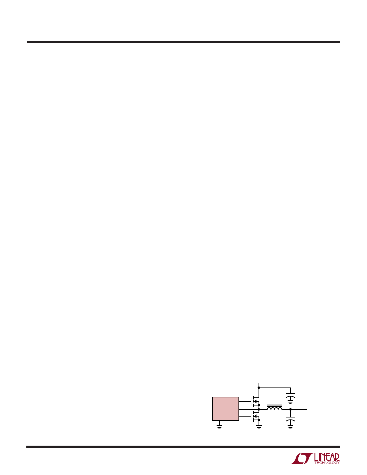
Switching Architecture
Each half of the LTC1703 is designed to operate as a
synchronous buck converter (Figure 1). Each channel
includes two high power MOSFET gate drivers to control
external N-channel MOSFETs QT and QB. These drivers
have 0.5Ω output impedances and can carry well over an
amp of continuous current with peak currents up to 5A to
slew large MOSFET gates quickly. The external MOSFETs
are connected with the drain of QT attached to the input
supply and the source of QT at the switching node SW. QB
is the synchronous rectifier with its drain at SW and its
source at PGND. SW is connected to one end of the
inductor, with the other end connected to V
capacitor is connected from V
to PGND.
OUT
. The output
OUT
When a switching cycle begins, QB is turned off and QT is
turned on. SW rises almost immediately to VIN and the
inductor current begins to increase. When the PWM pulse
finishes, QT turns off and one nonoverlap interval later, QB
turns on. Now SW drops to PGND and the inductor current
decreases. The cycle repeats with the next tick of the
master clock. The percentage of time spent in each mode
is controlled by the duty cycle of the PWM signal, which in
turn is controlled by the feedback amplifier. The master
clock runs at a 550kHz rate and turns QT once every 1.8µs.
In a typical application with a 5V input and a 1.5V output,
the duty cycle will be set at 1.5/5 × 100% or 30% by the
feedback loop. This will give roughly a 540ns on-time for
QT and a 1.26µs on-time for QB.
V
IN
+
C
L
TG
LTC1703BGSW
PGND
Figure 1. Synchronous Buck Architecture
QT
EXT
QB
IN
V
+
OUT
C
OUT
1703 F01
10
+
TG
BOOST
SW
BG
PGND
PV
CC
D
CP
C
IN
+
C
OUT
1703 F02
V
OUT
L
EXT
V
IN
QT
QB
C
CP
1µF
LTC1703
WUUU
APPLICATIO S I FOR ATIO
This constant frequency operation brings with it a couple
of benefits. Inductor and capacitor values can be chosen
with a precise operating frequency in mind and the feedback loop components can be similarly tightly specified.
Noise generated by the circuit will always be in a known
frequency band with the 550kHz frequency designed to
leave the 455kHz IF band free of interference. Subharmonic
oscillation and slope compensation, common headaches
with constant frequency current mode switchers, are
absent in voltage mode designs like the LTC1703.
During the time that QT is on, its source (the SW pin) is at
VIN. VIN is also the power supply for the LTC1703. However, QT requires VIN + V
minimum RON. This presents a problem for the LTC1703—
it needs to generate a gate drive signal at TG higher than
its highest supply voltage. To accomplish this, the TG
driver runs from floating supplies, with its negative supply
attached to SW and its power supply at BOOST. This
it to slew up and down with the source of QT. In combination
with a simple external charge pump (Figure 2),
the LTC1703 to completely enhance the gate of QT without
requiring an additional, higher supply voltage.
The two channels of the LTC1703 run from a common
clock, with the phasing chosen to be 180° from side 1 to
side 2. This has the effect of doubling the frequency of the
switching pulses seen by the input bypass capacitor,
significantly lowering the RMS current seen by the capacitor and reducing the value required (see the 2-Phase
section).
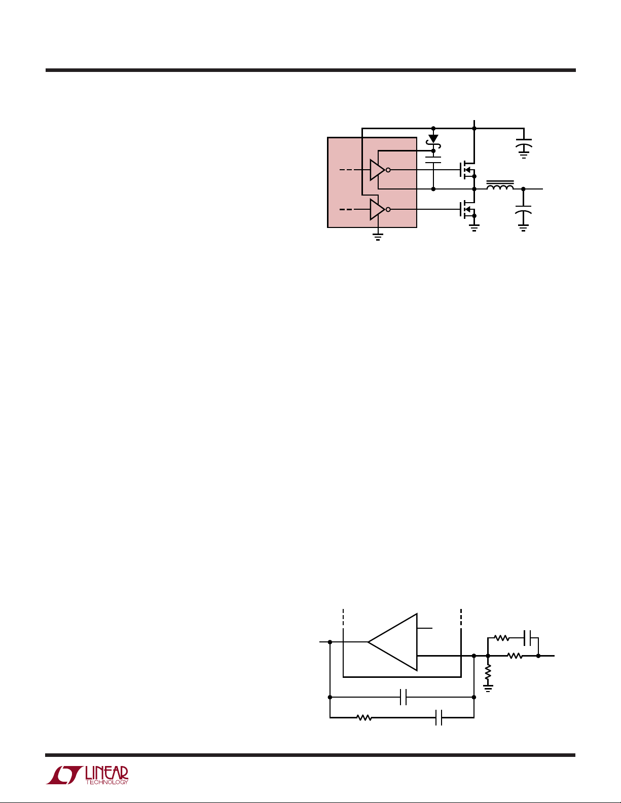
Feedback Amplifier
Each side of the LTC1703 senses the output voltage at
V
with an internal feedback op amp (see Block Dia-
OUT
gram). This is a real op amp with a low impedance output,
85dB open-loop gain and 25MHz gain-bandwidth product.
The positive input is connected internally to an 800mV
reference, while the negative input is connected to the FB
pin. The output is connected to COMP, which is in turn
connected to the soft-start circuitry and from there to the
PWM generator.
Unlike many regulators that use a resistor divider connected to a high impedance feedback input, the LTC1703
is designed to use an inverting summing amplifier
at its gate to achieve
GS(ON)
allows
this allows
LTC1703
Figure 2. Floating TG Driver Supply
topology with the FB pin configured as a virtual ground.
This allows flexibility in choosing pole and zero locations
not available with simple gm configurations. In particular,
it allows the use of “type 3” compensation, which provides a phase boost at the LC pole frequency and significantly improves loop phase margin (see Figure 3). The
Feedback Loop/Compensation section contains a detailed explanation of type 3 feedback loops. Note that side
1 of the LTC1703 includes R1 and RB internally as part
of the VID DAC circuitry.
MIN/MAX COMPARATORS
Two additional feedback loops keep an eye on the primary
feedback amplifier and step in if the feedback node moves
±5% from its nominal 800mV value. The MAX comparator
(see Block Diagram) activates whenever FB rises more
than 5% above 800mV. It immediately turns the top
MOSFET (QT) off and the bottom MOSFET (QB) on and
keeps them that way until FB falls back within 5% of its
nominal value. This pulls the output down as fast as possible, preventing damage to the (often expensive) load. If
FB rises because the output is shorted to a higher supply,
QB will stay on until the short goes away, the higher supply
0.8V
COMP
R2
Figure 3. “Type 3” Feedback Loop (Side 2 Shown)
+
FB
–
C2
FB
R
C1
1703 F03
C3
R3
R1
B
V
OUT
11
 Loading...