

Linear Technology LTC1701 Datasheet
Final Electrical Specifications
FEATURES
■
Tiny 5-Lead SOT-23 Package
■
Uses Tiny Capacitors and Inductor
■
High Frequency Operation: 1MHz
■
High Output Current: 500mA
■
Low R
■
High Efficiency: Up to 94%
■
Current Mode Operation for Excellent Line
Internal Switch: 0.28Ω
DS(ON)
and Load Transient Response
■
Short-Circuit Protected
■
Low Quiescent Current: 135µA
■
Low Dropout Operation: 100% Duty Cycle
■
Ultralow Shutdown Current: IQ < 1µA
■
Peak Inductor Current Independent of Inductor Value
■
Output Voltages from 5V Down to 1.25V
U
APPLICATIO S
LTC1701
1MHz Step-Down
DC/DC Converter in SOT-23
December 1999
U
DESCRIPTIO
The LTC®1701 is the industry’s first 5-lead SOT-23 step
down, current mode, DC/DC converter. Intended for small
to medium power applications, it operates from 2.5V to
5.5V input voltage range and switches at 1MHz, allowing
the use of tiny, low cost capacitors and inductors 2mm or
less in height. The output voltage is adjustable from 1.25V
to 5V. A built-in 0.28Ω switch allows up to 0.5A of output
current at high efficiency. OPTI-LOOPTM compensation
allows the transient response to be optimized over a wide
range of loads and output capacitors.
The LTC1701 incorporates automatic power saving Burst
ModeTM operation to reduce gate charge losses when the
load current drops below the level required for continuous
operation. With no load, the converter draws only 135µA.
In shutdown, it draws less than 1µA, making it ideal for
current sensitive applications.
■
PDAs/Palmtop PCs
■
Digital Cameras
■
Cellular Phones
■
Portable Media Players
■
PC Cards
■
Handheld Equipment
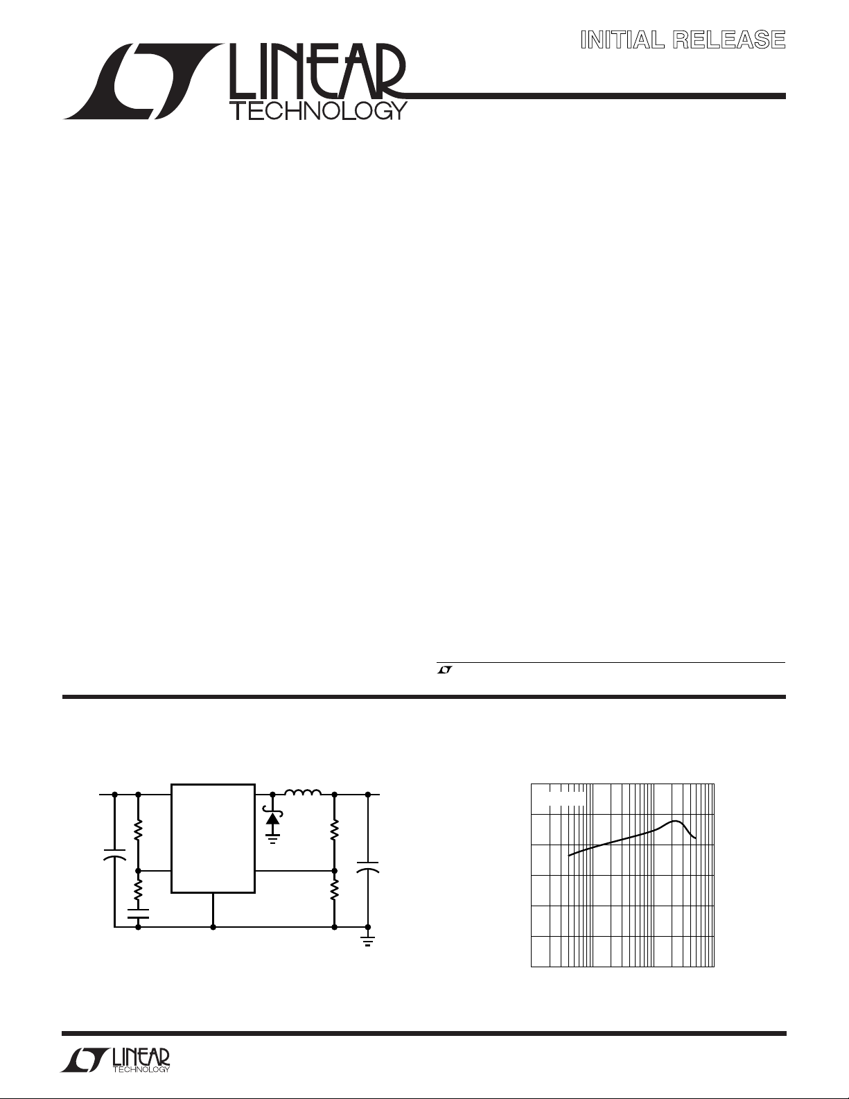
TYPICAL APPLICATIO
V
IN
2.5V TO
5.5V
+
C1
10µF
C1: TAIYO YUDEN JMK316BJ106ML
C2: SANYO POSCAP 6TPA47M
D1: MBRM120L
L1: SUMIDA CD43-4R7
Figure 1. Step-Down 2.5V/500mA Regulator
R4
1M
R3
5.1k
C3
330pF
V
IN
LTC1701
ITH/RUN
GND
SW
V
FB
U
4.7µH
D1
In dropout, the internal P-channel MOSFET switch is
turned on continuously, thereby maximizing battery life.
Its small size and switching frequency enables the complete DC/DC converter function to consume less than 0.3
square inches of PC board area.
, LTC and LT are registered trademarks of Linear Technology Corporation.
Burst Mode and OPTI-LOOP are trademarks of Linear Technology Corporation.
L1
R2
121k
R1
121k
V
OUT
(2.5V/
500mA)
+
C2
47µF
1701 F01
100
95
90
85
EFFICIENCY (%)
80
75
70
1 10 100 1000
Efficiency Curve
VIN = 3.3V
LOAD CURRENT (mA)
1701 F01a
Information furnished by Linear Technology Corporation is believed to be accurate and reliable.
However, no responsibility is assumed for its use. Linear Technology Corporation makes no representation that the interconnection of its circuits as described herein will not infringe on existing patent rights.
1

LTC1701
WW
W
ABSOLUTE AXI U RATI GS
U
UUW
PACKAGE/ORDER I FOR A TIO
(Note 1)
(Voltages Referred to GND Pin)
VIN Voltage (Pin 5).......................................–0.3V to 6V
ITH/RUN Voltage (Pin 4) ..............................–0.3V to 3V
VFB Voltage (Pin 3) ......................................–0.3V to 3V
Peak Switch Current (Pin 1) ................................... 1.3A
VIN – SW (Max Switch Voltage)................8.5V to –0.3V
Operating Temperature Range (Note 2).. –40°C to 85°C
Junction Temperature (Note 5).............................125°C
TOP VIEW
SW 1
GND 2
3
V
FB
S5 PACKAGE
5-LEAD PLASTIC SOT-23
T
= 125°C, θJA = 110°C/W
JMAX
5 V
IN
4 ITH/RUN
ORDER PART
NUMBER
LTC1701ES5
S5 PART
MARKING
LTKG
Storage Temperature Range................. –65°C to 150°C
Lead Temperature (Soldering, 10 sec)..................300°C
Consult factory for Industrial and Military grade parts.
ELECTRICAL CHARACTERISTICS
temperature range, otherwise specifications are at TA = 25°C. V
specified. (Note 2)
SYMBOL PARAMETER CONDITIONS MIN TYP MAX UNITS
V
IN
I
FB
V
FB
∆V
LINE REG
∆V
LOAD REG
V
ITH/RUN
I
ITH/RUN
I
SW(PEAK)
R
DS(ON)
I
SW(LKG)
t
OFF
Operating Voltage Range 2.5 5.5 V
Feedback Pin Input Current (Note 3) ±0.1 µA
Feedback Voltage (Note 3) ● 1.22 1.25 1.28 V
Reference Voltage Line Regulation VIN = 2.5V to 5V (Note 3) 0.04 0.1 %/V
Output Voltage Load Regulation Measured in Servo Loop, V
Input DC Supply Current (Note 4)
Active Mode V
Sleep Mode V
Shutdown V
Run Threshold High I
Run Threshold Low I
Run Pullup Current V
Peak Switch Current Threshold VFB = 0V 0.9 1.1 A
Switch ON Resistance VIN = 5V, VFB = 0V 0.28 Ω
Switch Leakage Current VIN = 5V, V
Switch Off-Time 400 500 600 ns
The ● denotes the specifications which apply over the full operating
= 3.3V, R
IN
Measured in Servo Loop, V
= 0V 185 300 µA
FB
= 1.4V 135 200 µA
FB
= 0V 0.25 1 µA
ITH/RUN
Ramping Down 1.4 1.6 V
TH/RUN
Ramping Up 0.3 0.6 V
TH/RUN
= 1V 50 100 300 µA
ITH/RUN
= 3.3V, VFB = 0V 0.30 Ω
V
IN
V
= 2.5V, VFB = 0V 0.35 Ω
IN
= 0V, VFB = 0V 0.01 1 µA
ITH/RUN
= 1Meg (from VIN to ITH/RUN) unless otherwise
ITH/RUN
= 1.5V, (Note 3) 0.01 0.70 %
ITH
= 1.9V, (Note 3) –0.80 –1.50 %
ITH
Note 1: Absolute Maximum Ratings are those values beyond which the life
of a device may be impaired.
Note 2: The LTC1701E is guaranteed to meet performance specifications
from 0°C to 70°C. Specifications over the –40°C to 85°C operating
temperature range are assured by design, characterization and correlation
with statistical process controls.
2
Note 3: The LTC1701 is tested in a feedback loop which servos VFB to the
midpoint for the error amplifier (V
Note 4: Dynamic supply current is higher due to the internal gate charge
being delivered at the switching frequency.
Note 5: T
according to the following formula:
is calculated from the ambient TA and power dissipation P
J
LTC1701ES5: T
= TA + (PD•110°C/W)
J
= 1.7V unless otherwise specified).
ITH
D
UUU
PI FU CTIO S
LTC1701
SW (Pin 1): The Switch Node Connection to the Inductor.
This pin swings from VIN to a Schottky diode (external)
voltage drop below ground. The cathode of the Schottky
diode must be closely connected to this pin.
GND (Pin 2): Ground Pin. Connect to the (–) terminal of
C
, the Schottky diode and (–) terminal of CIN.
OUT
VFB (Pin 3): Receives the feedback voltage from the
external resistive divider across the output. Nominal volt-
ITH/RUN (Pin 4): Combination of Error Amplifier Compensation Point and Run Control Input. The current comparator threshold increases with this control voltage. Nominal
voltage range for this pin is 1.25V to 2.25V. Forcing this
pin below 0.8V causes the device to be shut down. In
shutdown all functions are disabled.
VIN (Pin 5): Main Supply Pin and the (+) Input to the
Current Comparator. Must be closely decoupled to ground.
age for this pin is 1.25V.
Pin Limit Table
NOMINAL (V) ABSOLUTE MAX (V)
PIN NAME DESCRIPTION MIN TYP MAX MIN MAX
1 SW Switch Node –0.3 V
2 GND Ground Pin 0
3VFBOutput Feedback Pin 0 1.25 1.35 –0.3 3
4I
/RUN Error Amplifier Compensation and RUN Pin 0 2.25 –0.3 3
TH
5VINMain Power Supply 2.5 5.5 –0.3 6
–0.3 VIN + 0.3
IN
BLOCK DIAGRA
REF
REF
+
I
TH
CLAMP
–
+
ERROR
AMP
–
1.4V
/REF
+
OVER
VOLTAGE
COMP
–
ITH/RUN
V
V
V
FB
W
V
IN
50µA
SHDN
(1.25V TO 2.25V)
PULSE
STRETCHER
<0.6V
V
FB
1.5V
V
IN
1.25V
BANDGAP
REFERENCE
+
–
I
TH
COMP
V
REF
(1.25V)
CURRENT
COMP
+
–
CONTROL LOGIC
V
REF
OFF-TIMER
AND GATE
CURRENT
SENSE
AMP
GATE
DRIVER
V
IN
+
–
SW
GND
1701 BD
3

LTC1701
fO=
−
+
VV
VV T
IN OUT
IN D OFF
1
OPERATIO
U
The LTC1701 uses a contant off-time, current mode
architecture. The operating frequency is then determined
by the off-time and the difference between VIN and V
To optimize efficiency, the LTC1701 automatically switches
between continuous and Burst Mode operation.
The output voltage is set by an external divider returned to
the VFB pin. An error amplfier compares the divided output
voltage with a reference voltage of 1.25V and adjusts the
peak inductor current accordingly.
Main Control Loop
During normal operation, the internal PMOS switch is
turned on when the VFB voltage is below the reference
voltage. The current into the inductor and the load increases until the current limit is reached. The switch turns
off and energy stored in the inductor flows through the
external Schottky diode into the load. After the constant
off-time interval, the switch turns on and the cycle repeats.
The peak inductor current is controlled by the voltage on
the ITH/RUN pin, which is the output of the error
amplifier.This amplifier compares the VFB pin to the 1.25V
reference. When the load current increases, the FB voltage
decreases slightly below the reference. This decrease
causes the error amplifier to increase the ITH/RUN voltage
until the average inductor current matches the new load
current.
OUT
.
The main control loop is shut down by pulling the ITH/RUN
pin to ground. When the pin is released an external resistor
is used to charge the compensation capacitor. When the
voltage at the ITH/RUN pin reaches 0.8V, the main control
loop is enabled and the error amplifier drives the ITH/RUN
pin. Soft-start can be implemented by ramping the voltage
on the ITH/RUN pin (see Applications Information section).
Low Current Operation
When the load is relatively light, the LTC1701 automatically switches to Burst Mode operation in which the
internal PMOS switch operates intermittently based on
load demand. The main control loop is interrupted when
the output voltage reaches the desired regulated value.
The hysteretic voltage comparator trips when ITH/RUN is
below 1.5V, shutting off the switch and reducing the
power consumed. The output capacitor and the inductor
supply the power to the load until the output voltage drops
slightly and the ITH/RUN pin exceeds 1.5V, turning on the
switch and the main control loop which starts another
cycle.
Dropout Operation
In dropout, the internal PMOS switch is turned on continuously (100% duty cycle) providing low dropout operation
with V
an under voltage lockout, care should be taken to shut
down the LTC1701 for VIN < 2.5V.
at VIN. Since the LTC1701 does not incorporate
OUT
U
WUU
APPLICATIO S I FOR ATIO
The basic LTC1701 application circuit is shown in
Figure 1. External component selection is driven by the
load requirement and begins with the selection of L1. Once
L1 is chosen, the Schottky diode D1 can be selected
followed by CIN and C
L Selection and Operating Frequency
The operating frequency is fixed by VIN, V
constant off-time of about 500ns. The complete expression for operating frequency is given by:
4
OUT
.
OUT
and the
Although the inductor does not influence the operating
frequency, the inductor value has a direct effect on ripple
current. The inductor ripple current ∆IL decreases with
higher inductance and increases with higher VIN or V
∆=
I
L
−
VVfLVV
IN OUT OUT D
VV
IN D
+
+
OUT
:
 Loading...