

FEATURES
■
Operates from Single Li-Ion Battery
■
2.8V to 5.5V Input Voltage Range
■
Very Low Shutdown Current: <2µA
■
Synchronous Buck Architecture for High Efficiency
■
PWM Dimming Frequency Adjustable with a Single
Capacitor
■
Accurate Lamp Current Maximizes Lamp Lifetime
■
Fixed Frequency Operation at 300kHz
■
Internal or External PWM Dimming
■
Small 10-Pin MSOP Package
U
APPLICATIO S
■
PDAs
■
Handheld Computers
■
Portable Instruments
■
Handheld GPS with Map Display
■
Handheld TV/Video Monitor
LTC1697
High Efficiency Low Power
1W CCFL Switching Regulator
U
DESCRIPTIO
®
The LTC
cathode fluorescent lamp (CCFL). An internal PWM dimming system maximizes efficiency and dimming range.
Accurate lamp currents can be set with a single external
resistor.
The LTC1697 includes a synchronous current mode PWM
controller with internal 1A MOSFET switches. It contains
a 300kHz oscillator, 0.8V reference, and internal current
sense. It operates from a 2.8V to 5.5V input voltage. The
LTC1697 also has a thermal limit and a shutdown that
reduces supply current to <2µA.
The LTC1697 is available in the MSOP-10 package.
, LTC and LT are registered trademarks of Linear Technology Corporation.
Protected by U.S. Patent 6522116.
1697 is designed to control a single 1W cold
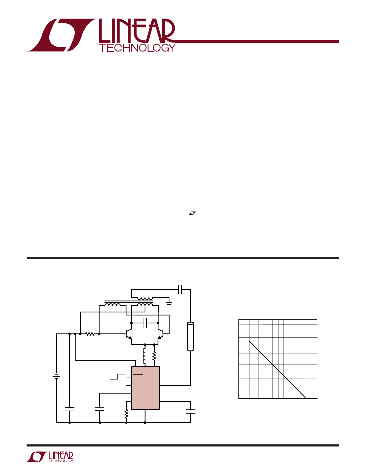
TYPICAL APPLICATIO
110234
V
2.8V TO 5.5V
+
Li-Ion
CELL
IN
330Ω
DIMMING INPUT
1V(0%) – 2V(100%)
0.022µF10µF
OFF ON
U
65
0.15µF
33µH
VIN SW 0V
SHDN
LTC1697
V
DIM
C
DIM
R
PROG
GND
8.25k
LAMP
SEN
V
C
200k
27pF
1kV
CCFL
LAMP
0.1µF
1697 TA01
10
9
8
7
6
5
(mA)
4
CCFL
I
3
2
4k 10k 20k6k 8k
I
CCFL
vs R
R
PROG
PROG
(Ω)
1967 TA01b
1697f
1
LTC1697
1
2
3
4
5
C
DIM
V
DIM
0V
SEN
SW
GND
10
9
8
7
6
SHDN
R
PROG
V
C
V
IN
LAMP
TOP VIEW
MS PACKAGE
10-LEAD PLASTIC MSOP
WW
W
ABSOLUTE AXI U RATI GS
U
UUW
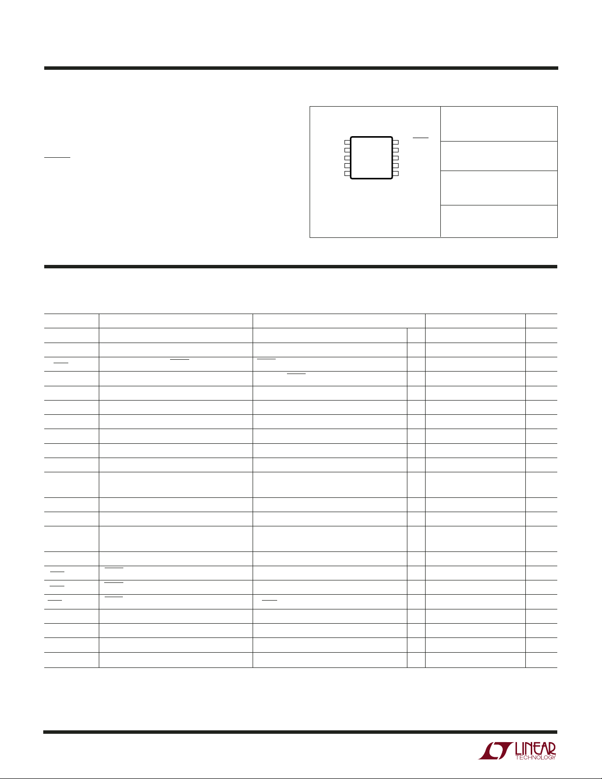
PACKAGE/ORDER I FOR ATIO
(Notes 1, 2)
VIN Voltage .................................................. –0.5V to 6V
VC, OV
Voltages ................................... –0.5V to (V
SHDN, V
, C
SEN
DIM
, R
DIM
Pins ......................................... –0.5V to 6V
PROG
, SW
+ 0.3V)
IN
ORDER PART
NUMBER
LTC1697EMS
LAMP Pin ................................................. –0.5V to 0.5V
Operating Temperature Range (Note 5) ...–40°C to 85°C
T
Storage Temperature Range ..................–65°C to 125°C
Lead Temperature (Soldering, 10 sec).................. 300°C
θ
JA
Consult LTC Marketing for parts specified with wider operating temperature ranges.
ELECTRICAL CHARACTERISTICS
The ● denotes the specifications which apply over the full operating
temperature range, otherwise specifications are at TA = 25°C. 2.8V < VIN ≤ 5.5V unless otherwise specified.
SYMBOL PARAMETER CONDITIONS MIN TYP MAX UNITS
V
IN
V
UVLO
I
Q-SHDN
I
Q-Active
I
LEAK
R
ON
I
MAX
% DC Duty Cycle ● 095%
f
SWITCH
f
DIM
V
DIM
I
DIM
R
LAMP
I
L(ERROR)
R
P(RANGE)
V
SHDN-H
V
SHDN-L
I
SHDN
I
OVSEN
V
OVSEN
V
DIM(SD-I)
V
DIM(SD-H)
Operating Supply Voltage Range (Note 2) ● 2.8 5.5 V
Undervoltage Lockout ● 2.77 V
Quiescent Current - SHDN SHDN = 0V; V
= 0V 1 2 µA
DIM
Quiescent Current - Active VC = 0V, SHDN = VIN = V
Switch Leakage 0.1 1 µA
Switch On Resistance VIN = 4V 0.18 Ω
Switch Current Limit ● 0.9 1.6 A
Switching Frequency ● 240 300 370 kHz
Dimming PWM Frequency C
V
Input Voltage Dimming PWM Duty Cycle = 0% 1.0 V
DIM
= 0.022µF (Note 3) ● 190 250 310 Hz
DIM
Dimming PWM Duty Cycle = 100% 2.0 V
V
Input Bias Current V
DIM
Internal R
Resistance LAMP Pin to GND 50 60 Ω
LAMP
Lamp Current Accuracy |1– I
= 2V ±1 µA
DIM
/(32/6.4k)| • 100% (Note 6) ● 26 %
= 5mA
I
LAMP
LAMP(AVG)
Programming Resistor Range (Note 10) ● 6.4 16 kΩ
SHDN Input High 1.2 V
SHDN Input Low (Note 9) 0.4 V
SHDN Input Current V
Overvoltage Sense Protect Current (Note 7) I
SHDN
LAMP
= V
IN
= 5mA, R
= 6.4k ● 16.65 21.5 26.35 µA
PROG
Overvoltage Sense Pin Voltage ● 0.95 1.2 1.5 V
Passive Shutdown Voltage (Note 8) ● 0.4 V
Not in Passive Shutdown ● 1.05 V
= 125°C,
JMAX
= 160°C/W 1 LAYER BOARD
= 4.2V (Note 4) 0.9 1.5 mA
DIM
● 0.1 1 µA
MS PART MARKING
LTZR
1697f

ELECTRICAL CHARACTERISTICS
LTC1697
Note 1: Absolute Maximum Ratings are those values beyond which the life
of a device may be impaired.
Note 2: All voltages specified with respect to GND pin.
Note 3: The dimming PWM frequency is set by the equation 5Hz/C
Note 4: Actual operating current will be higher due to lamp operating
current.
Note 5: The LTC1697 is guaranteed to meet performance specifications
from 0°C to 70°C. Specifications over the –40°C to 85°C operating
temperature range are assured by design, characterization and correlation
with statistical process controls.
U
UU
DIM
(µF).
PI FU CTIO S
C
(Pin 1): Dimming Capacitor. Connect the pin to GND
DIM
with a 0.022µF capacitor (nominal). The value of capaci-
tance on the C
frequency. The transfer function of capacitance to frequency is 5Hz/C
V
(Pin 2): Dimming Control Pin. The V
DIM
the duty cycle of the dimming PWM. It ranges from 0% at
V
= 1V to 100% at V
DIM
<0.4V the LTC1697 will enter shutdown mode after ≈50ms.
0V
(Pin 3): Overvoltage Sense Pin. Protects the high-
SEN
voltage transformer from the overvoltage condition that
occurs when the lamp is open or not present. This pin is
connected through a resistor to the emitters of the drive
transistors of the Royer oscillator.
SW (Pin 4): Switch Pin. Connect the inductor and optional
Schottky diode here. Minimize trace length to keep EMI
and high frequency ringing down.
pin determines the dimming PWM
DIM
(µF).
DIM
pin controls
DIM
= 2V. If the V
DIM
voltage is
DIM
Note 6: I
LAMP(AVG)
positive and negative lamp current flowing into and out of the LAMP pin.
Note 7: For currents at or above I
0%.
Note 8: At V
the SHDN pin was pulled low.
Note 9: To minimize I
Note 10: 2mA ≤ I
= the average of the magnitude (absolute value) of the
, the switch duty cycle will be
the LTC1697 behaves as if
voltages below V
DIM
shutdown, pull the SHDN pin below 0.1V.
Q
≤ 5mA.
LAMP
OVSEN(ON)
DIM(SHDNON)
GND (Pin 5): Signal and Power Ground for the LTC1697.
LAMP (Pin 6): Lamp Current Feedback Pin. Connect this
pin to the CCFL lamp.
VIN (Pin 7): Input Supply Pin.
VC (PIN 8): Compensation Node. Connect this pin to GND
through a 0.1µF capacitor. See Application Information
section. A frequency compensation network is connected
to this pin to compensate the loop. See the section “V
C
Compensation” for guidelines.
R
(Pin 9): Lamp Current Programming. Connect this
PROG
pin to GND with a 6.4k 1% resistor (nominal). See Application Information section for resistor selection.
SHDN (Pin 10): Shutdown. Grounding this pin shuts down
the LTC1697. Tie to >1V to enable.
1697f
3

LTC1697
BLOCK DIAGRA
W
TO ROYER
OSCILLATOR
SHDN
10
SHUTDOWN
ANTI
SHOOTTHRU
PROTECTION
PWM
LOGIC
SW
4
N
CURRENT
LIMIT
CURRENT
COMP
200k
V
IN
7
2.8V
TO 5.5V
I
SENSE
AMP
0V
SEN
3
+
1.6A
–
TYP
–
+
+
–
Σ
TRANSFORMER
VOLTAGE
PROTECTION
V
C
8
0.8V
–
GND
PWM
+
OSC
5
DIMMING
OSC
1
C
2V
1V
0.7V
DIM
SLOPE
COMP
+
+
–
I
R
PROG
50Ω
LAMP
LAMP
FB
–
2
V
DIM
1697 BD
9
6
R
PROG
LAMP
R
P
1697f

WUUU
APPLICATIO S I FOR ATIO
LTC1697
Background
Current generation handheld computers and instruments
typically use backlit liquid crystal displays (LCDs). Cold
cathode fluorescent lamps (CCFLs) provide the highest
available efficiency for backlighting the display, where
providing the most light out for the least amount of input
power is the most important goal. These lamps require
high voltage AC to operate, mandating an efficient high
voltage DC/AC converter. The lamps operate from DC, but
migration effects damage the lamp and shorten its lifetime. Lamp drive should ideally contain zero DC component. In addition to good efficiency, the converter should
deliver the lamp drive in the form of a sine wave. This
minimizes EMI and RF emissions, which can interfere with
other devices and degrade overall operating efficiency.
Sinusoidal CCFL drive also maximizes current-to-light
conversion in the lamp. The circuit also permits lamp
intensity control from zero to full brightness with no
hysteresis or “pop-on.”
The small size and battery-powered operation associated
with LCD-equipped apparatus dictate low component
count and high efficiency for these circuits. Size constraints place severe limitations on circuit architecture and
long battery life is usually a priority. Handheld portable
computers offer an excellent example. The CCFL and its
power supply can be responsible for almost 50% of the
total battery drain.
The CCFL regulator drives an inductor that acts as a
switch-mode current source for a current-driven Royerclass converter with efficiencies as high as 90%. The
control loop forces the CCFL PWM to modulate the average inductor current to maintain constant current in the
lamp. This constant current and the resulting lamp intensity is programmable. Lamp intensity is further controlled
by modulating the current to the Royer converter at 150Hz
to 500Hz.
Operation
The LTC1697 is a fixed frequency, current mode regulator.
Such a switcher controls switch duty cycle directly by
switch current rather than by output voltage. Referring to
the block diagram for the LTC1697, the NMOS switch
turns ON at the start of each oscillator cycle. The NMOS
switch turns back OFF when switch current reaches a
predetermined level.
Current Sensing
Lossless current sensing converts the peak current signal
to a voltage which is summed with the internal slope
compensation. This summed signal is compared to VC to
provide a peak current control command for the PWM.
Current Limit
The current limit amplifier will shut the NMOS switch off
once the current exceeds the current limit threshold. The
current amplifier delay to the output is typically 50ns.
Synchronous Rectifier
The LTC1697 operates as a synchronous converter. When
the NMOS switch turns OFF as mentioned above, the
PMOS switch turns ON. This gives a low resistance current
path for the inductor current back to VIN.
Dimming PWM
An on-chip PWM dimming circuit enables and disables the
current mode regulator for each dimming cycle. It also
disconnects the feedback network from the compensation
node (VC) to reduce slew time at the next enable time. The
oscillator for the dimming PWM produces a triangle wave
whose frequency is determined by an external capacitor
on the C
5Hz/C
pin. The dimming PWM frequency is equal to
DIM
(µF) with its duty cycle set by the voltage on the
DIM
1697f
5

LTC1697
WUUU
APPLICATIO S I FOR ATIO
V
pin where DC = 0% at V
DIM
V
= 2V. If desired, the internal dimming PWM can be
DIM
overridden by grounding the C
input PWM signal to the V
signal should be in the range of 150Hz to 500Hz.
Lamp Feedback
In a typical application, the LAMP pin is connected to the
low voltage side of the lamp. The lamp pin is internally
connected to ground by a ~50Ω resistor. This resistor will
limit the voltage on the LAMP pin to ±0.35V for a 5mA
lamp current. The lamp feedback circuit removes a current
from VC approximating 1/40 of the absolute value of the
current through the 50Ω resistor.
Current Programming Input (R
The I
current is set with an external resistor con-
LAMP
nected between this pin and ground. I
VC Compensation
The VC node is the point where the lamp feedback current,
the programming current, and the control for the switching controller meet. A single capacitor must be connected
from the VC pin to ground to compensate the feedback
loop. Careful consideration should be given to the value of
capacitance used. A large value (1µF) will give excellent
stability at high lamp currents but will result in degraded
line regulation. On the other hand, a small value (10nF) will
result in overshoot and poor load regulation. The value
chosen will depend on the maximum load current and
dimming range. After these parameters are decided upon,
the value of the VC capacitor should be increased until the
= 1V and DC = 100% at
DIM
pin and applying the
DIM
pin. This external PWM
DIM
)
PROG
= 32V/R
LAMP
RMS
PROG
.
line regulation becomes unacceptable. A typical value for
the VC capacitor is 0.1µF. For further information on
compensation please refer to Application Note 65 or
consult the factory.
OV
Operation
SEN
The OV
pin can be used to protect the high voltage
SEN
transformer from an overvoltage condition that can occur
when the lamp is open or not present. Connect this pin
through a resistor to the emitters of the drive transistors
of the Royer oscillator. The voltage at the OV
specified by V
. The duty cycle of the LTC1697 SW pin
OVSEN
will be 0% when the current flowing out of the OV
reaches I
(protect). See the manufacturers trans-
OVSEN
SEN
pin is
pin
SEN
former specifications for transformer voltage ratings.
Thermal Shutdown
This IC includes overtemperature protection that is intended to protect the device during momentary overload
conditions. Junction temperature will exceed 125°C when
overtemperature protection is active. Continuous operation above the specified maximum operating junction
temperature may result in device degradation or failure.
Shutdown Operation
There are two ways to place the LTC1697 in shutdown. The
SHDN pin can be pulled below V
be pulled below V
DIM(SD-I)
for more than approximately
SHDN-1
, or the V
DIM
pin can
50mS. For normal operation, both pins must be pulled
high. The SHDN pin must be pulled above V
V
pin must be pulled above V
DIM
DIM (SD-H)
SHDN-H
, and the
.
1697f

PACKAGE DESCRIPTIO
U
MS Package
10-Lead Plastic MSOP
(Reference LTC DWG # 05-08-1661)
0.889 ± 0.127
± .005)
(.035
LTC1697
5.23
(.206)
MIN
0.305
± 0.038
± .0015)
(.0120
TYP
RECOMMENDED SOLDER PAD LAYOUT
0.254
(.010)
GAUGE PLANE
0.18
(.007)
NOTE:
1. DIMENSIONS IN MILLIMETER/(INCH)
2. DRAWING NOT TO SCALE
3. DIMENSION DOES NOT INCLUDE MOLD FLASH, PROTRUSIONS OR GATE BURRS.
MOLD FLASH, PROTRUSIONS OR GATE BURRS SHALL NOT EXCEED 0.152mm (.006") PER SIDE
4. DIMENSION DOES NOT INCLUDE INTERLEAD FLASH OR PROTRUSIONS.
INTERLEAD FLASH OR PROTRUSIONS SHALL NOT EXCEED 0.152mm (.006") PER SIDE
5. LEAD COPLANARITY (BOTTOM OF LEADS AFTER FORMING) SHALL BE 0.102mm (.004") MAX
3.20 – 3.45
(.126 – .136)
DETAIL “A”
DETAIL “A”
0.50
(.0197)
BSC
° – 6° TYP
0
0.53 ± 0.152
(.021 ± .006)
SEATING
PLANE
3.00 ± 0.102
(.118 ± .004)
(NOTE 3)
4.90 ± 0.152
(.193 ± .006)
(.043)
0.17 – 0.27
(.007 – .011)
TYP
1.10
MAX
12
0.50
(.0197)
BSC
8910
3
7
6
45
0.497 ± 0.076
(.0196 ± .003)
REF
3.00 ± 0.102
(.118 ± .004)
(NOTE 4)
0.86
(.034)
REF
0.127 ± 0.076
(.005 ± .003)
MSOP (MS) 0603
Information furnished by Linear Technology Corporation is believed to be accurate and reliable.
However, no responsibility is assumed for its use. Linear Technology Corporation makes no representation that the interconnection of its circuits as described herein will not infringe on existing patent rights.
1697f
7

LTC1697
TYPICAL APPLICATIO
U
External PWM Dimming
RELATED PARTS
V
IN
2.8V TO 5.5V
+
Li-Ion
CELL
1V TO 2V
C1
10µF
C1: TAIYO YUDEN JMK212BJ106MM
C2: PANASONIC ECH-U1H154JC9
L1:SUMIDA CDRH6D28-330NC
110234
R1
330Ω
0V
OFF ON
150Hz TO
500Hz
Q1 Q2
33µH
8.25k
Q1, Q2: ZETEX FMMT-617
R1: 330Ω,1206 PKG
T1: SUMIDA CLQ122-S-227-5316
65
T1
C2
0.15µF
L1
VIN SW 0V
SHDN
LTC1697
V
DIM
C
DIM
R
PROG
GND
LAMP
SEN
V
200k
C
C3
27pF
1kV
CCFL
LAMP
C4
0.1µF
1697 TA02
PART NUMBER DESCRIPTION COMMENTS
LT1170/LT1170HV 5A, 100kHz High Efficiency Switching Regulator VIN: 3V to 40V/60V, V
I
= <50µA, N8, S16, TO220-5, DD Packages
SD
LT1182/LT1183 CCFL/LCD Contrast Switching Regulators, CCFL VIN: 3V to 30V, V
OUT(MAX)
Switch: 1.25A, LCD Switch: 625mA SO-16 Package
LT1184/LT1184F 1.25A, 200kHz, CCFL Current Mode Switching Regulator VIN: 3V to 30V, V
OUT(MAX)
SO-16 Package
LT1186/LT1186F 1.25A, 100kHz, DAC Programmable CCFL VIN: 4.5V to 30V, V
OUT(MAX)
Current Mode Switching Regulator SO-16 Package
LT1372/LT1372HV/ 1.5A, 500kHz/1MHz, High Efficiency Switching Regulator VIN: 2.7V to 30V, V
OUT(MAX)
LT1377 N8, S8 Packages
LT1373/LT1373HV 1.5A, 250kHz High Efficiency Switching Regulator VIN: 0.5V to 5V, V
OUT(MAX)
can Regulate Positive or Negative Outputs N8, S8 Packages
LT1768 High Power CCFL Controller for Wide Dimming Range VIN: 8V to 24V, V
OUT(MAX)
and Maximum Lamp Lifetime SSOP-16 Package
LT1786F 1.25A, 200kHz, SMBus Controlled CCFL Switching Regulator VIN: 4.5V to 30V, V
OUT(MAX)
Precision 100mA Full Scale Current SO-16 Package
= 65V/75V, IQ = 6mA,
OUT(MAX)
= 60V, IQ = 6mA, ISD = 35µA,
= 60V, IQ = 6mA, ISD = 35µA,
= 60V, IQ = 6mA, ISD = 35µA
= 35V, IQ = 4mA, ISD = <12µA
= 35V, IQ = 1mA, ISD = <12µA
= 28V, IQ = 7mA, ISD = 65µA
= 60V, IQ = 6mA, ISD = 150µA
Linear Technology Corporation
1630 McCarthy Blvd., Milpitas, CA 95035-7417
(408) 432-1900 ● FAX: (408) 434-0507 ● www.linear.com
1697f
LT/TP 1004 1K • PRINTED IN USA
© LINEAR TECHNOLOGY CORPORATION 2004
 Loading...