

FEATURES
■
±2% Overvoltage Threshold Accuracy
■
Low Profile (1mm) ThinSOTTM Package
■
Gate Drive for SCR Crowbar or External N-Channel
Disconnect MOSFET
■
Monitors Two Output Voltages
■
Senses Output Voltages from 0.8V to 24V
■
Wide Supply Range: 2.7V to 27V
■
Multifunction TIMER/RESET Pin
LTC1696
Overvoltage Protection
Controller
U
DESCRIPTIO
The LTC®1696 is a standalone power supply overvoltage
monitor and protection device designed to protect a power
supply load in the event of an overvoltage fault. It monitors
two adjustable output voltages. If an overvoltage condition is detected, the output drives either an external SCR
crowbar or turns off external back-to-back N-channel
MOSFETs, thereby, disconnecting the input voltage from
the power supply.
U
APPLICATIO S
■
Telecommunication Systems
■
Computer Systems
■
Industrial Control Systems
■
Notebook Computers
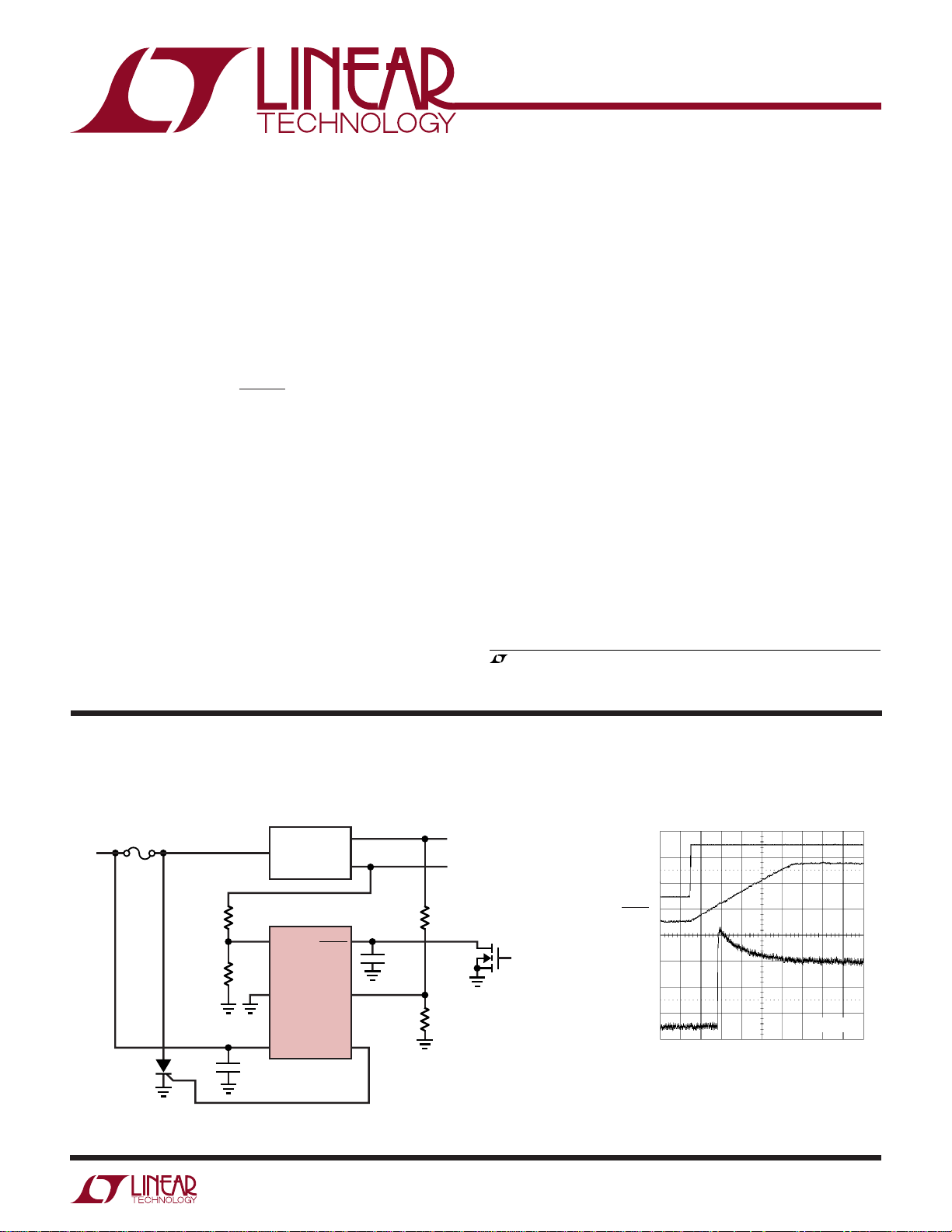
TYPICAL APPLICATIO
SCR Crowbar
V
CC
12V
POWER
SUPPLY
U
Pin 6 offers three functions. By connecting a capacitor to
this pin, the internal glitch filter time delay can be programmed. Without the capacitor, the default time delay is
determined by an internal capacitor. This pin also serves
as a reset input to clear the internal latch after an overvoltage fault condition. By pulling it high, the OUT pin is
activated if the FB1 and FB2 voltages remain below the trip
threshold.
The LTC1696 is available in the low profile (1mm) ThinSOT
package.
, LTC and LT are registered trademarks of Linear Technology Corporation.
ThinSOT is a trademark of Linear Technology Corporation.
Overvoltage Response
V
OUT2
5V
V
OUT1
3.3V
FB1
0.5V/DIV
SCR
2N6507
137k
1%
44.2k
1%
R2
1
FB1
R1
C2
0.1µF
LTC1696
2
GND
3
V
CC
TIMER/
RESET
FB2
OUT
6
5
4
1696 TA01
C1
1nF
R4
232k
1%
2N7002
R3
44.2k
1%
TIMER/RESET
2V/DIV
Q1
RESET
I
OUT
20mA/DIV
100µs/DIV
C1 = 1nF
1696 TA02
1
LTC1696
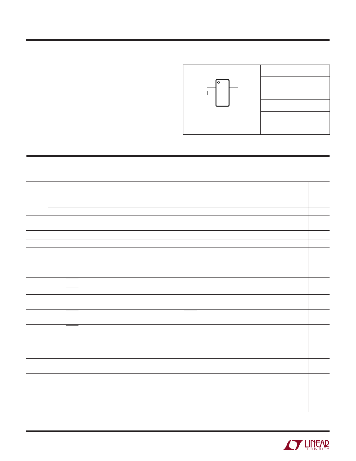
PACKAGE/ORDER I FOR ATIO
UU
W
FB1 1
GND 2
V
CC
3
6
5 FB2
4 OUT
TOP VIEW
TIMER/
RESET
S6 PACKAGE
6-LEAD PLASTIC SOT-23
WWWU
ABSOLUTE AXI U RATI GS
(Note 1)
Supply Voltage (VCC) ............................................... 28V
Input Voltage
FB1, FB2 ............................................... –0.3V to 17V
TIMER/RESET .......................................–0.3V to 17V
Operating Temperature Range (Note 2) .. –40°C to 85°C
Storage Temperature Range ................. –65°C to 150°C
Lead Temperature (Soldering, 10 sec)..................300°C
ORDER PART NUMBER
LTC1696ES6
S6 PART MARKING
T
= 125°C, θJA = 256°C/W
JMAX
Consult LTC Marketing for parts specified with wider operating temperature
ranges.
LTLT
ELECTRICAL CHARACTERISTICS
temperature range, otherwise specifications are at TA = 25°C. 2.7V ≤ VCC ≤ 27V (Notes 3, 4) unless otherwise noted.
SYMBOL PARAMETER CONDITIONS MIN TYP MAX UNITS
V
CC
I
VCC
V
FB
I
FB
V
FBHST
V
LKO
V
LKH
V
RST
V
TIM
V
TRIG
I
TRIG
I
TIM
V
OUTH
V
OUTL
t
OVPD1
t
OVPD2
2
Supply Voltage Range Operating Range ● 2.7 27 V
Standby Supply Current FB1, FB2 < V
Active Supply Current FB1, FB2 > VFB, C
FB1, FB2 Feedback Threshold Voltage Going Positive TA ≥ 0°C ● 0.862 0.880 0.898 V
FB1, FB2 Input Current ● – 1 – 0.05 µA
FB1, FB2 Feedback Hysteresis High-to-Low Transition 12 mV
VCC Undervoltage Lockout FB1, FB2 > V
Low-to-High Transition ● 1.75 2.05 2.35 V
High-to-Low Transition
VCC Undervoltage Lockout Hysteresis FB1, FB2 > V
TIMER/RESET Reset Low Threshold FB1, FB2 > V
TIMER/RESET Timer High Threshold FB1, FB2 > V
TIMER/RESET External Trigger High FB1, FB2 < V
Threshold
TIMER/RESET External Trigger High FB1, FB2 < VFB, TIMER/RESET = V
Current
TIMER/RESET Timer Current FB1 = (VFB + 30mV), FB2 < V
OUT High Voltage 12V ≤ VCC ≤ 27V, FB1, FB2 > VFB, C
OUT Low Voltage FB1, FB2 < VFB, I
OUT Propagation Delay for FB1 FB1 > VFB, FB2 < VFB, TIMER/RESET = Open, ● 728 µs
OUT Propagation Delay for FB2 FB2 > VFB, FB1 < VFB, TIMER/RESET = Open, ● 728 µs
The ● denotes the specifications which apply over the full operating
FB
OUT
FB
FB
FB
FB
FB
FB1 = (V
FB2 = (V
FB2 = (V
FB1, FB2 = (V
V
CC
C
OUT
C
OUT
+ 200mV), FB2 < V
FB
+ 30mV), FB1 < V
FB
+ 200mV), FB1 < V
FB
+ 200mV) ● 81840 µA
FB
= 3.3V, FB1, FB2 > VFB, C
SINK
= 1000pF
= 1000pF
● 170 540 µA
= 1000pF ● 1.1 3.5 mA
< 0°C ● 0.853 0.880 0.907 V
T
A
● 1.64 1.94 2.24 V
110 mV
● 0.78 0.865 0.95 V
● 1.11 1.185 1.26 V
● 1.35 1.50 1.65 V
TRIG
FB
FB
FB
FB
= 1000pF ● 4.8 6.3 8.0 V
OUT
= 1000pF ● 2.7 3.2 3.3 V
OUT
= 1mA, VCC = 3.3V ● 0.45 V
● 260 650 µA
● 41022 µA
● 51226 µA
● 41022 µA
● 51226 µA
LTC1696
ELECTRICAL CHARACTERISTICS
The ● denotes the specifications which apply over the full operating
temperature range, otherwise specifications are at TA = 25°C. 2.7V ≤ VCC ≤ 27V (Notes 3, 4) unless otherwise noted.
SYMBOL PARAMETER CONDITIONS MIN TYP MAX UNITS
t
OVPD1,2
t
r
I
OUTSC
Note 1: Absolute Maximum Ratings are those values beyond which the life
of the device may be impaired.
Note 2: The LTC1696E is guaranteed to meet performance specifications
from 0°C to 70°C. Specifications over the –40°C to 85°C operating
temperature range are assured by design, characterization and correlation
with statistical process controls.
OUT Propagation Delay for FB1, FB2 FB1, FB2 > VFB, TIMER/RESET = Open ● 624 µs
= 1000pF
C
OUT
OUT Rise Time FB1, FB2 > VFB, C
OUT Short-Circuit Current 12V ≤ VCC ≤ 27V, FB1, FB2 > VFB, ● 35 80 160 mA
Shorted to GND
V
OUT
VCC = 2.7V, FB1, FB2 > VFB, V
= 1000pF ● 0.4 3 µs
OUT
Shorted to GND ● 2918 mA
OUT
Note 3: All currents into device pins are positive; all currents out of device
pins are negative. All voltages are referenced to device ground unless
otherwise specified.
Note 4: All typical numbers are given for V
= 12V and TA = 25°C.
CC
3
LTC1696
SUPPLY VOLTAGE (V)
0
1.4
1.2
1.0
0.8
0.6
0.4
0.2
0
15 25
1696 G03
510
20 30
SUPPLY CURRENT (mA)
TA = 25°C
C
OUT
= 1000pF
UW
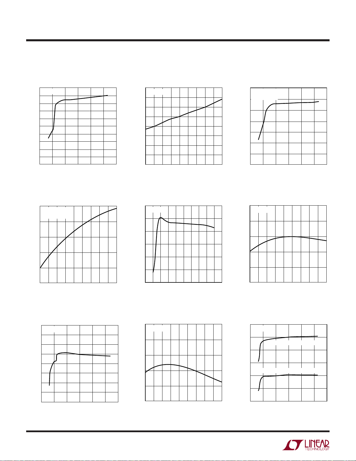
TYPICAL PERFOR A CE CHARACTERISTICS
Standby Supply Current
vs Supply Voltage
200
TA = 25°C
180
160
140
120
100
80
60
SUPPLY CURRENT (µA)
40
20
0
5
0
10
SUPPLY VOLTAGE (V)
Active Supply Current
vs Temperature
1.20
VCC = 12V
= 1000pF
C
OUT
1.15
1.10
1.05
SUPPLY CURRENT (mA)
1.00
15 20
Standby Supply Current
vs Temperature
200
VCC = 12V
190
180
170
160
150
SUPPLY CURRENT (µA)
140
130
30
25
1696 G01
120
–35 125
–55
–15
25
45
5
TEMPERATURE (°C)
65
105
85
1696 G02
FB1, FB2 Feedback Threshold
Voltage vs Supply Voltage
0.8814
TA = 25°C
0.8811
0.8808
0.8805
0.8802
0.8799
Active Supply Current
vs Supply Voltage
FB1, FB2 Feedback Threshold
Voltage vs Temperature
0.90
VCC = 12V
0.89
0.88
0.87
0.86
0.95
–55
TIMER Threshold Voltage
vs Supply Voltage TIMER Current vs Supply Voltage
1.200
1.195
1.190
1.185
1.180
1.175
1.170
TIMER THRESHOLD VOLTAGE (V)
1.165
1.160
0
4
–35 5
–15
TA = 25°C
510 20
25
TEMPERATURE (°C)
15
SUPPLY VOLTAGE (V)
85
45 125
105
65
1696 G04
25
1696 G07
FB1, FB2 FEEDBACK THRESHOLD VOLTAGE (V)
0.8796
6121824
SUPPLY VOLTAGE (V)
TIMER Threshold Voltage
vs Temperature
1.24
VCC = 12V
1.22
1.20
1.18
1.16
TIMER THRESHOLD VOLTAGE (V)
1.14
–35 5
–15
30
–55
TEMPERATURE (°C)
85
45 125
65
25
1696 G05
105
1696 G08
FB1, FB2 FEEDBACK THRESHOLD VOLTAGE (V)
0.85
–35 5
–15
3030 9 15 21 27
–55
20
TA = 25°C
18
16
14
12
TIMER CURRENT (µA)
10
FB1 OR FB2 OVERDRIVE = 200mV
8
0
5
25
TEMPERATURE (°C)
FB1 AND FB2 OVERDRIVE = 200mV
10 15 20
SUPPLY VOLTAGE (V)
85
45 125
105
65
1696 G06
25 30
1696 G09

UW
FEEDBACK OVERDRIVE (mV)
0
4
TIMER CURRENT (µA)
6
8
10
12
14
16
50 100 150 200
1696 G12
250
VCC = 3.3V
T
A
= 25°C
FB1 AND FB2 OVERDRIVE
FB1 OR FB2 OVERDRIVE
SUPPLY VOLTAGE (V)
0
1.51
1.50
1.49
1.48
1.47
1.46
1.45
1.44
15 25
1696 G15
510
20 30
EXTERNAL TRIGGER TRESHOLD VOLTAGE (V)
TA = 25°C
TYPICAL PERFOR A CE CHARACTERISTICS
LTC1696
TIMER Current vs Temperature
22
VCC = 12V
20
18
16
14
12
TIMER CURRENT (µA)
10
8
–55
FB1 AND FB2 OVERDRIVE = 200mV
FB1 OR FB2 OVERDRIVE = 200mV
–35 –15 5 25 45 125
TEMPERATURE (°C)
Glitch Filter Timer
vs Feedback Overdrive
25
VCC = 3.3V
T
= 25°C
A
20
15
10
GLITCH FILTER TIMER (µs)
5
FB1 OR FB2 OVERDRIVE
FB1 AND FB2 OVERDRIVE
65 85 105
1696 G10
TIMER Current
vs Feedback Overdrive
20
VCC = 12V
T
= 25°C
A
16
12
8
TIMER CURRENT (µA)
4
0
50
0
FEEDBACK OVERDRIVE (mV)
Glitch Filter Timer
vs Feedback Overdrive
30
VCC = 12V
= 25°C
T
A
25
20
15
10
GLITCH FILTER TIMER (µs)
5
FB1 AND FB2 OVERDRIVE
FB1 OR FB2 OVERDRIVE
150
100
FB1 OR FB2 OVERDRIVE
FB1 AND FB2 OVERDRIVE
200
TIMER Current
vs Feedback Overdrive
250
1696 G11
External Trigger Threshold
Voltage vs Supply Voltage
0
50
0
FEEDBACK OVERDRIVE (mV)
100
External Trigger Threshold
Voltage vs Temperature
1.505
VCC = 12V
1.500
1.495
1.490
1.485
EXTERNAL TRIGGER THRESHOLD VOLTAGE (V)
1.475
1.480
–35 5
–55
–15
TEMPERATURE (°C)
150
200
45 125
65
25
0
0
250
1696 G13
50 100 150 200
FEEDBACK OVERDRIVE (mV)
RESET Threshold Voltage
vs Supply Voltage
0.868
TA = 25°C
0.866
0.864
0.862
0.860
0.858
0.856
RESET THRESHOLD VOLTAGE (V)
0.854
85
105
1696 G16
0.852
510 20
0
SUPPLY VOLTAGE (V)
15
250
1696 G14
RESET Threshold Voltage
vs Temperature
0.880
VCC = 12V
0.875
0.870
0.865
0.860
0.855
0.850
RESET TRHESHOLD VOLTAGE (V)
0.845
0.840
25
30
1696 G17
–35 125
–55
–15
25
45
5
TEMPERATURE (°C)
65
105
85
1696 G18
5

LTC1696
OUTPUT VOLTAGE (V)
0
0
ACTIVE OUTPUT CURRENT (mA)
10
30
40
50
100
70
2
4
5
1696 G24
20
80
90
60
1
3
6
7
TA = 25°C
VCC = 27V
VCC = 12V
UW
TYPICAL PERFOR A CE CHARACTERISTICS
OUT Pin Active Output Voltage
vs Supply Voltage
8
TA = 25°C
= 1000pF
C
OUT
7
6
5
4
3
2
1
OUT PIN ACTIVE OUTPUT VOLTAGE (V)
0
510 20
0
15
SUPPLY VOLTAGE (V)
OUT Pin Short-Circuit Current
vs Temperature
120
100
80
60
V
OUT
VCC = 27V
VCC = 12V
SHORTED TO GND
OUT Pin Active Output Voltage
vs Temperature
6.6
6.5
6.4
6.3
6.2
6.1
6.0
5.9
OUT PIN ACTIVE OUTPUT VOLTAGE (V)
5.8
25
30
1696 G19
–35 125
–55
–15
25
5
TEMPERATURE (°C)
45
VCC = 12V
= 1000pF
C
OUT
65
85
105
1696 G20
OUT Pin Active Output Current
vs Output Voltage
30
25
20
= 5V
V
15
CC
TA = 25°C
OUT Pin Short-Circuit Current
vs Supply Voltage
100
90
80
70
60
50
40
30
20
10
OUT PIN SHORT-CIRCUIT CURRENT (mA)
0
5
0
TA = 25°C
SHORTED TO GND
V
OUT
15 20
10
SUPPLY VOLTAGE (V)
OUT Pin Active Output Current
vs Output Voltage
30
25
1696 G21
40
20
OUT PIN SHORT-CIRCUIT CURRENT (mA)
0
–35 5
–55
6
–15
25
TEMPERATURE (°C)
VCC = 5V
VCC = 2.7V
85
45 125
105
65
1696 G22
10
ACTIVE OUTPUT CURRENT (mA)
5
0
VCC = 2.7V
1234
OUTPUT VOLTAGE (V)
50.50 1.5 2.5 3.5 4.5
1696 G23

LTC1696
U
UU
PI FU CTIO S
FB1 (Pin 1): First Feedback Input. FB1 monitors and
senses the first supply output voltage through an external
resistor divider. This voltage is then compared with an
internal reference voltage of 0.88V, which sets the threshold for an overvoltage fault detection. If the sense voltage
exceeds the threshold level, the output response time at
the OUT pin is dependent on the feedback overdrive above
the threshold level. The higher the feedback overdrive, the
faster will be the response time.
GND (Pin 2): Power Ground. Return path for all device
currents.
VCC (Pin 3): Power Supply. The pin is connected separately from the power supply output that the chip is
monitoring. Its input range is from 2.7V to 27V. The
quiescent current is typically 100µA in standby mode
when the device is operating at 5V. The quiescent current
increases to 170µA when operating at 12V.
OUT (Pin 4): Output Current Limit Driver. Capable of
delivering continuous current, typically 80mA, at high
supplies. The output current decreases with lower supply
voltage. This pin directly drives the SCR crowbar at high
supply voltage. It can also provide gate drive for an
N-channel MOSFET or the base of an NPN transistor,
which drives the gate of an external SCR at low supply
voltage. It is normally in the inactive low state in the
standby mode. In the event of an overvoltage fault condition, the OUT pin is latched into the active high state. The
latched active high state is reset by pulling the TIMER/
RESET pin low through an N-channel MOSFET switch or if
the supply voltage at the VCC pin goes below the undervoltage lockout threshold voltage of 1.94V.
FB2 (Pin 5): Second Feedback Input. FB2 monitors and
senses the second supply output voltage through an
external resistor divider. This voltage is then compared
with an internal reference voltage of 0.88V, which sets the
threshold for an overvoltage fault detection. If the sense
voltage exceeds the threshold level, the output response
time at the OUT pin is dependent on the feedback overdrive
above the threshold level. The higher the feedback overdrive, the faster will be the response time.
TIMER/RESET (Pin 6): Glitch Filter Timer Capacitor, Reset
and External Trigger Input. The external capacitor connected to this pin programs the internal glitch filter time
delay. The internal current source used to charge the timer
capacitor is typically 10µA with feedback overdrive of less
than 20mV above the feedback trip threshold from one
feedback input. The current source increases to 12µA
when the feedback overdrive increases to more than
100mV. It further increases to 18µA if larger overdrive
occurs from both feedback inputs. The default glitch filter
time delay without an external timer capacitor is fixed by
an internal capacitor of 5pF with the internal reference
voltage of 1.185V. The delay reduces with increases in first
and second feedback input overdrive. This pin also serves
as a reset input to clear the internal latch during an
overvoltage fault condition. If pulled low, it resets the
active high state of the internal latch. The reset signal to
this pin should be an open drain type. This pin can also be
driven high externally to activate the OUT pin active high
if the FB1 and FB2 voltages remain below the feedback trip
threshold.
7

LTC1696
BLOCK DIAGRA
V
3
CC
W
R3R4
INTERNAL 5V SUPPLY
R2
+
+
V
REF
–
–
R1
OUT
4
2V
GND
FB1
FB2
2
1
5
+
+
UVLO
GLITCH
FILTER
LOGIC
–
BANDGAP
+
REFERENCE
–
0.88V
WUUU
APPLICATIO S I FOR ATIO
Feedback Inputs
The LTC1696 has two feedback inputs that allow monitoring of two output voltages. The trip point of the internal
comparator is set by an internal reference of 0.88V with
±2% accuracy. The output voltage, VS, is sensed through
an external resistor divider network (Figure 1). The resistors R1 and R2 values are calculated with the typical trip
point of 0.88V.
–
1.185V
INTERNAL 5V SUPPLY
+
+
0.865V
–
V
S
R2
R1
FB1
1696 BD
LTC1696
+
10µA +
FUNCTION
OF FB1 AND FB2
OVERDRIVE
6
TIMER/
RESET
–
+
V
= 0.88V
REF
–
R
1
V
088
=•.
RR
12
+
R
2
=
S
–. •
VR
088 1
()
S
.
088
As an example, let’s calculate values for R1 and R2 for a
3.3V supply in which an overvoltage indication is required
8
Figure 1
at +10% (3.63V). First, a value for R1 is chosen based on
the allowable resistor divider string current. This is determined by power dissipation requirements and possible
sensitivity to noise coupling into the resistor divider. In
this exercise, assume the resistor divider current is 20µA.
R1 is calculated from:

WUUU
APPLICATIO S I FOR ATIO
V
R
1
FB
I
DIVIDER
088
.
20
V
k
44==µ=
A
The time delay is given by:
t
D
CV
1•
=
I
LTC1696
INT
CHG
The nearest 1% value for R1 is 44.2k. Now, calculating for
R2 yields:
kVV
44 2 3 63 0 88
.•. –.
R
()
V
088
.
=
k2
138 1=
.
Choosing the nearest 1% value yields 137k.
The chosen values for R1 and R2 yield an overvoltage
threshold of 3.608V (+ 9.3%). With worst-case tolerances
applied, the minimum overvoltage threshold is 3.481V
(+ 5.5%) and the maximum overvoltage threshold is 3.738V
(+13.3%).
Reset Function
In the event of an overvoltage condition, the OUT pin of the
LTC1696 is latched into an active high state. The internal
latch is reset by pulling the TIMER/RESET pin low through
an external N-channel MOSFET switch or pulling V
CC
voltage below the UVLO trip point of 1.94V.
Glitch Filter Timer
The LTC1696 has a programmable glitch filter to prevent
the output from entering its active high latched condition
if transients occur on the FB1 or FB2 pins. The filter time
delay is programmed externally by an external capacitor
C1 connected to the TIMER/RESET pin.
where V
I
CHG
capacitor C1. The current source I
is the internal reference voltage of 1.185V and
INT
is the internal current source charging the external
charging the
CHG
external timer capacitor is 10µA for small feedback
transients and increases to 12µA for large feedback
transients (greater than 100mV) from one feedback
input. The charging current increases to 18µA for large
feedback transients from both feedback inputs.
SCR Crowbar
The LTC1696 can deliver continuous output current typically 80mA at high supply voltage to trigger an external
SCR crowbar in the event of an overvoltage condition as
shown in the typical application on the front page of the
data sheet. The output current decreases when the supply
voltage reduces. It delivers 25mA at a supply voltage of 5V.
At a low supply voltage of 3.3V, the output current reduces
to 10mA and an external NPN emitter follower is needed to
boost the current in order to drive the SCR crowbar as
shown in Figure 2. The power dissipation due to the high
output current at high supply voltage can potentially
exceed the thermal limit of the package. This is avoided by
resetting the device rapidly when the external SCR crowbar has been triggered, so that the device is not kept in the
active high state for too long.
V
OUT2
V
CC
3.3V
R2
54.9k
1%
R1
44.2k
1%
Q1
2N3904
R5
5%
R6
22Ω
5%
470Ω
Figure 2. External SCR with NPN Emitter Follower with Low Voltage Supplies
SCR
2N6507
C2
0.1µF
POWER
SUPPLY
1
FB1
LTC1696
2
GND
3
V
CC
TIMER/
RESET
FB2
OUT
6
C1
1nF
5
4
1696 F02
2.5V
V
1.8 V
R4
93.1k
1%
2N7002
R3
44.2k
1%
OUT1
Q1
RESET
9

LTC1696
WUUU
APPLICATIO S I FOR ATIO
Back-to-Back N-Channel MOSFET
A power management circuit that uses the LTC1696 to
control external back-to-back N-channel MOSFET at low
supply voltage is shown in Figure 3. In standby mode, the
drain of the external N-channel MOSFET, Q1, is pulled high
R2
38.3k
1.5V
V
3.3V
1%
R1
44.2k
1%
CC
C2
0.1µF
1
FB1
LTC1696
2
GND
3
V
CC
TIMER/
RESET
FB2
OUT
6
C1
1nF
5
4
POWER MANAGEMENT
by the power management controller when the LTC1696
OUT pin is in the low state. The LTC1696 drives the gate of
Q1 high during an overvoltage fault condition. This pulls
the drain of Q1 low and turns off the back-to-back Nchannel MOSFETs.
2N7002
R3
44.2k
54.9k
1%
PRIMARY
INPUT
SUPPLY
CONTOLLER
Q2
R4
1%
RESET
1.8V
N-CHANNEL
×2
Q1
2N7002
1696 F03
Figure 3. Back-to-Back N-Channel MOSFETs for Low Supply Application
10

PACKAGE DESCRIPTIO
LTC1696
U
S6 Package
6-Lead Plastic SOT-23
(LTC DWG # 05-08-1634)
(LTC DWG # 05-08-1636)
2.80 – 3.10
(.110 – .118)
(NOTE 3)
SOT-23
(Original)
.90 – 1.45
A
(.035 – .057)
.00 – 0.15
A1
(.00 – .006)
.90 – 1.30
A2
(.035 – .051)
.35 – .55
L
(.014 – .021)
.20
(.008)
DATUM ‘A’
L
NOTE:
1. CONTROLLING DIMENSION: MILLIMETERS
2. DIMENSIONS ARE IN
3. DRAWING NOT TO SCALE
4. DIMENSIONS ARE INCLUSIVE OF PLATING
5. DIMENSIONS ARE EXCLUSIVE OF MOLD FLASH AND METAL BURR
6. MOLD FLASH SHALL NOT EXCEED .254mm
7. PACKAGE EIAJ REFERENCE IS:
SC-74A (EIAJ) FOR ORIGINAL
JEDEC MO-193 FOR THIN
SOT-23
(ThinSOT)
1.00 MAX
(.039 MAX)
.01 – .10
(.0004 – .004)
.80 – .90
(.031 – .035)
.30 – .50 REF
(.012 – .019 REF)
MILLIMETERS
(INCHES)
2.60 – 3.00
(.102 – .118)
.09 – .20
(.004 – .008)
(NOTE 2)
1.50 – 1.75
(.059 – .069)
(NOTE 3)
A
PIN ONE ID
.95
(.037)
REF
A2
1.90
(.074)
REF
.25 – .50
(.010 – .020)
(6PLCS, NOTE 2)
A1
S6 SOT-23 0401
Information furnished by Linear Technology Corporation is believed to be accurate and reliable.
However, no responsibility is assumed for its use. Linear Technology Corporation makes no representation that the interconnection of its circuits as described herein will not infringe on existing patent rights.
11

LTC1696
WUUU
APPLICATIO S I FOR ATIO
External Triggering
The LTC1696 has a feature which allows the output to be
latched into an active high state by pulling the TIMER/
RESET pin high even if both the feedback voltages at the
R2
38.3k
1.5V
V
3.3V
1%
R1
44.2k
1%
CC
C2
0.1µF
1
FB1
LTC1696
2
GND
3
V
CC
TIMER/
RESET
FB2
OUT
6
5
4
POWER MANAGEMENT
FB1 and FB2 pins are below the trip threshold of the
internal comparator. The output is then reset by pulling the
TIMER/RESET pin low. Figure 4 shows a circuit that uses
the external triggering function of the LTC1696.
5V
C1
1nF
54.9k
R3
44.2k
1%
PRIMARY
INPUT
SUPPLY
CONTOLLER
2N7002
R4
1%
D1
1N4148
Q2
1.8V
RESET
2N7002
Q3
Q1
2N7002
1696 F04
R5
6.8k
5%
TRIGGER
N-CHANNEL
×2
Figure 4. External Triggering
RELATED PARTS
PART NUMBER DESCRIPTION COMMENTS
LTC1473 Dual PowerPathTM Switch Driver For Systems with Multiple DC Sources, VIN Up to 30V, Inrush and
Short-Circuit Protection
LTC1628 High Efficiency, 2-Phase Synchronous Step-Down Out-of-Phase Controllers, 3.5V ≤ VIN ≤ 36V,
Switching Regulator ±1% Output Voltage Accuracy
LT1681 Dual Transistor Synchronous Forward Controller Operation Up to 72V Maximum
LTC1698 Secondary Synchronous Rectifier Controller Optocoupler Feedback with Pulse Transformer Synchronization
LTC1703 Dual 550k Synchronous 2-Phase Switching Two Independent PWM Controllers, Wide Load Current Range,
Regulator Controller with VID 1.5% Output Accuracy
LTC1735 Synchronous Step-Down Switching Regulator Current Mode, 3.5V ≤ VIN ≤ 36V, 0.5V ≤ V
LTC1922-1 Synchronous Phase Modulated Full-Bridge Controller Output Power Levels from 50W to Several kW, Adaptive
DirectSense
TM
Zero Voltage Switching
LTC1960 Dual Battery Charger/Selector with SPI Interface Extends Run Time, Reduces Charging Time, Crisis Management
Prevents Power Interruption, 36-Pin SSOP
PowerPath and DirectSense are trademarks of Linear Technology Corporation.
OUT
≤ 5V
12
Linear Technology Corporation
1630 McCarthy Blvd., Milpitas, CA 95035-7417
(408) 432-1900 ● FAX: (408) 434-0507
●
www.linear.com
1696f LT/TP 0701 2K • PRINTED IN USA
LINEAR TECHN OLOGY CORPORATION 2001
 Loading...