

Linear Technology LTC1695 Datasheet
FEATURES
■
Complete SMBus/I2CTM Brushless DC Fan Speed
Control System in a 5-Pin SOT-23 package
■
0.75Ω PMOS Linear Regulator with 180mA
Output Current Rating
■
0V to 4.922V Output Voltage Range Controlled by a
6-Bit DAC
■
Simple 2-Wire SMBus/I2C Interface
■
250ms Internal Timer Ensures Fan Start-Up
■
Current Limit and Thermal Shutdown
■
Fault Status Indication via SMBus Host Readback
U
APPLICATIO S
■
Notebook Computers
■
Spot Cooling
■
Portable Instruments
■
Battery-Powered Systems
■
DC Motor Control
■
White LED Power Supplies
■
Programmable Low Dropout Regulator
, LTC and LT are registered trademarks of Linear Technology Corporation.
2
C is a trademark of Philips Electronics N.V.
I
LTC1695
SMBus/I2C Fan Speed
Controller in SOT-23
U
DESCRIPTIO
The LTC®1695 fan speed controller provides all the functions necessary for a power management microprocessor
to regulate the speed of a 5V brushless DC fan via a 2-wire
SMBus/I2C interface. Fan speed is controlled according to
the system’s required temperature profile and permits
lower fan power consumption, longer battery run time and
lower acoustical generated noise versus systems that
only provide simple on-off control for the fan.
The LTC1695 incorporates a 180mA low dropout linear
regulator, a 2-wire SMBus/I2C interface and a 6-bit DAC.
Fan speed is controlled by varying the fan’s terminal
voltage through the output voltage of the LTC1695’s linear
regulator. The LTC1695’s output voltage is programmed
by sending a 6-bit digital code to the LTC1695 DAC via the
SMBus. To eliminate fan start-up problems at lower fan
voltages, users can enable the LTC1695’s boost start
feature that provides the DAC’s full-scale output voltage
for 250ms before decreasing to the programmed output
voltage.
The LTC1695 includes output current limiting and thermal
shutdown as well as status monitors that can be read back
by the microprocessor during fault conditions. The
LTC1695 is available in a 5-lead SOT-23 package.
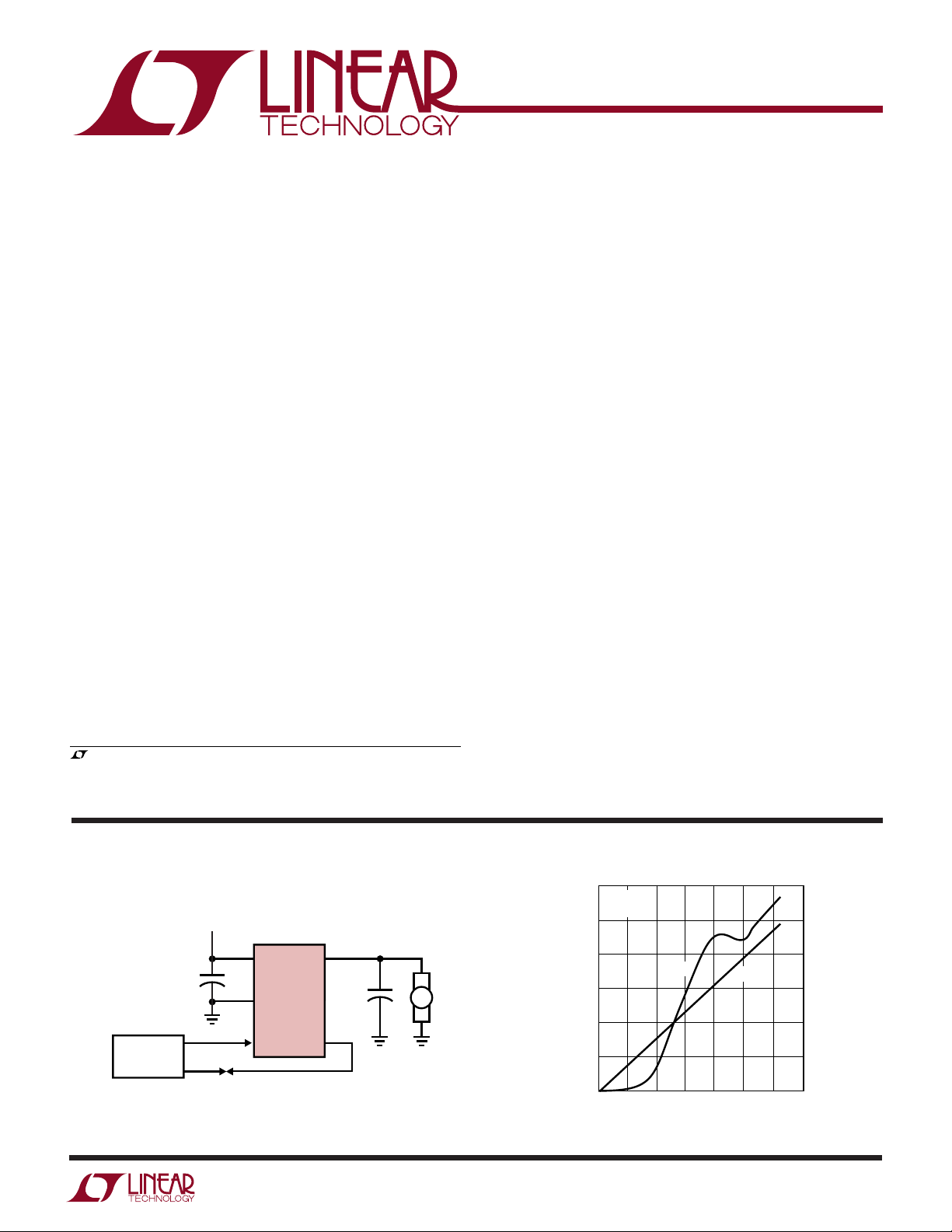
TYPICAL APPLICATION
5V
15
V
V
CC
+
10µF
2
3
SYSTEM
CONTROLLER
LTC1695
GND
SCL
OUT
SDA
U
4
4.7µF
Fan Voltage and Current vs DAC Code
120
VCC = 5V
= 25°C
T
A
100
80
+
5V DC FAN
SUNON
KDE0502PFB2-8
0.6W, 1.7 CFM
(25 • 25 • 10)mm
1695 • TA01
60
3
40
LOAD CURRENT (mA)
20
0
0
10 20
I
LOAD
40 60 70
30 50
DAC CODE
V
OUT
6
5
OUTPUT VOLTAGE (V)
4
3
2
1
0
1695 • TA02
1
LTC1695
WW
W
ABSOLUTE AXI U RATI GS
U
UUW
PACKAGE/ORDER I FOR ATIO
(Note 1)
Terminal Voltages
Supply Voltage (VCC) ............................................. 7V
All Other Inputs ........................ –0.3V to (V
+ 0.3V)
CC
Operating Temperature Range ..................... 0°C to 70°C
GND 2
SCL 3
Junction Temperature........................................... 125°C
Storage Temperature Range ..................–65°C to 150°C
Lead Temperature (Soldering, 10 sec)..................300°C
Consult factory for Industrial and Military grade parts.
ELECTRICAL CHARACTERISTICS
temperature range, otherwise specifications are at TA = 25°C. V
SYMBOL PARAMETER CONDITIONS MIN TYP MAX UNITS
V
CC
I
CC
DAC
V
LSB
V
OS
DNL Differential Nonlinearity I
INL Integral Nonlinearity I
V
FS
V
ZS
R
ON(P)
Timer and Thermal Shutdown
V
UVLO
T
BST_ST
T
THERMAL
I
FAULT
SMBus SCL, SDA Inputs
V
IH
V
IL
I
IN
C
IN
t
ON
t
OFF
V
OL
Supply Voltage Range 4.5 5 5.5 V
Supply Current, Operating V
Supply Current, Shutdown DAC Code = 0
DAC Resolution Guaranteed Monotonic ● 6 Bits
1LSB Resolution I
Offset Error I
V
, DAC Full Scale I
OUT
V
, DAC Zero Scale R
OUT
P-Channel On Resistance I
Undervoltage Lockout Voltage Rising V
Boost Start Timer I
Thermal Shutdown Temperature (Note 3) 155 °C
Output Current Limit Threshold V
Input High Threshold ● 2.1 V
Input Low Threshold ● 0.8 V
Input Current SCL, SDA = 0V or 5V ● ±0.1 ±5 µA
Input Capacitance (Note 3) 3 pF
Switch On Time from V
Stop Condition (f
Switch Off Time from V
Stop Condition (f
SDA Output Low Voltage I
= 100kHz) I
SMBus
= 100kHz) I
SMBus
The ● denotes the specifications which apply over the full operating
= 5V unless otherwise stated.
CC
= Full Scale, I
OUT
= 1mA ● 73 78 83 mV
LOAD
= 1mA ● ±1 LSB
LOAD
= 1mA (Note 2) ● ±0.75 LSB
LOAD
= 1mA (Note 2) ● ±0.75 LSB
LOAD
= 20mA ● 4.5 4.93 V
LOAD
= 150mA ● 4.5 4.9 V
I
LOAD
= 1kΩ ● 085 mV
LOAD
= 150mA 0.75 Ω
LOAD
CC
= 10mA, C
LOAD
= 0V, DAC Code = 63 ● 180 390 850 mA
OUT
from Zero Scale to Full Scale, ● 50 500 µs
OUT
= 1mA, C
LOAD
from Full Scale to Zero Scale, ● 150 500 µs
OUT
= 150mA, C
LOAD
= 3mA ● 150 400 mV
PULLUP
LOAD
= 4.7µF ● 75 250 1000 ms
LOAD
= 4.7µF
LOAD
LOAD
TOP VIEW
V
1
CC
S5 PACKAGE
5-LEAD PLASTIC SOT-23
T
= 125°C, θJA = 256°C/W
JMAX
SEE THE APPLICATIONS
INFORMATION SECTION.
= 150mA ● 150.7 155 mA
= 4.7µF
5 V
OUT
4 SDA
● 80 200 µA
● 2.3 2.9 3.5 V
ORDER PART
NUMBER
LTC1695CS5
S5 PART MARKING
LTIY
2
LTC1695
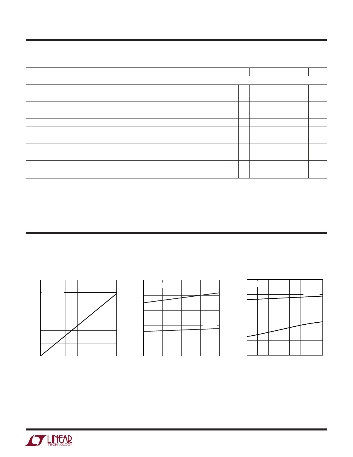
TEMPERATURE (°C)
–50
SUPPLY CURRENT (µA)
250
200
150
100
50
0
0
50
75
1695 • G03
–25
25
100
125
CODE 0
CODE 63
VCC = 5V
ELECTRICAL CHARACTERISTICS
temperature range, otherwise specifications are at TA = 25°C. V
The ● denotes the specifications which apply over the full operating
= 5V unless otherwise stated.
CC
SYMBOL PARAMETER CONDITIONS MIN TYP MAX UNITS
SMBus TIMING (Note 4)
f
SMB
t
BUF
t
HD(STA)
t
SU(STA)
t
SU(STO)
t
HD(DAT)
t
SU(DAT)
t
LOW
t
HIGH
t
f
t
r
Note 1: Absolute Maximum Ratings are those values beyond which the life
of a device may be impaired.
Note 2: INL, DNL specs are specified under a 1mA I
linear regulator from operating in dropout at higher DAC codes. DNL is
SMBus Operating Frequency ● 10 100 kHz
Bus Free Time Between Stop and Start ● 4.7 µs
Hold Time After (Repeated) Start Condition ● 4.0 µs
Repeated Start Condition Setup Time ● 4.7 µs
Stop Condition Setup Time ● 4.0 µs
Data Hold Time ● 300 ns
Data Setup Time ● 250 ns
Clock Low Period ● 4.7 µs
Clock High Period ● 4.0 50 µs
Clock/Data Fall Time ● 300 ns
Clock/Data Rise Time ● 1000 ns
Note 3: This typical specification is based on lab measurements and is not
production tested.
condition to keep the
LOAD
Note 4: Guaranteed by design and not tested. Please refer to the Timing
Diagram section for additional information.
measured from code 0 to code 63, taking into account the untrimmed offset
at code 0. Please refer to the Definitions section for more details.
UW
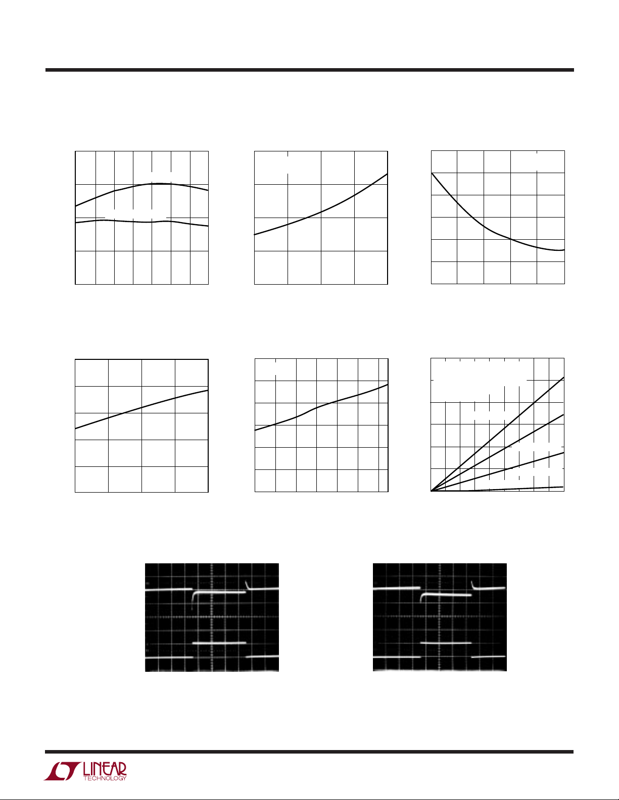
TYPICAL PERFOR A CE CHARACTERISTICS
Output Voltage vs
DAC Code
6
VCC = 5V
= 25°C
T
A
5
= 1mA
I
LOAD
4
3
2
OUTPUT VOLTAGE (V)
1
0
0
20 30 40
10
DAC CODE
50 60 63
1695 • G01
No Load Supply Current vs Supply
Voltage
250
TA = 25°C
200
150
100
SUPPLY CURRENT (µA)
50
0
4.0
4.5
5.0
SUPPLY VOLTAGE (V)
CODE 63
5.5
CODE 0
6.0
1695 • G02
No Load Supply Current vs
Temperature
3
LTC1695
TEMPERATURE (°C)
–50
OUTPUT VOLTAGE (V)
4.95
4.93
4.91
4.89
4.87
4.85
0
50
75
1695 • G09
–25
25
100
125
VCC = 5V
CODE 63
I
LOAD
= 1mA
I
LOAD
= 150mA
CODE
0
INL (LSB)
0.25
0.15
0.05
–0.05
–0.15
–0.25
10
20 30 40
1695 • G12
50 60 63
VCC = 5V
I
LOAD
= 1mA
UW
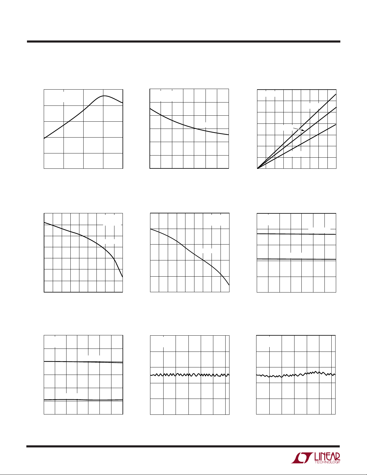
TYPICAL PERFOR A CE CHARACTERISTICS
Ground Current (Dropout Mode) vs
Supply Voltage
900
TA =25°C
I
= 180mA
LOAD
800
700
600
GROUND CURRENT (µA)
500
400
4.0
4.5
SUPPLY VOLTAGE (V)
CODE 63
5.0
Output Voltage (Full Scale) vs
Load Current
4.930
4.920
4.910
4.900
4.890
OUTPUT VOLTAGE (V)
4.880
4.870
5.5
VCC = 5V
= 25°C
T
A
CODE 63
1695 • G04
6.0
Ground Current (Dropout Mode)
vs Temperature
900
VCC = 5V
= 180mA
I
LOAD
850
800
750
700
GROUND CURRENT (µA)
650
600
–50
–25 0
TEMPERATURE (°C)
CODE 63
50 100 125
25 75
Output Voltage (Midscale) vs Load
Current
2.505
2.500
2.495
2.490
OUTPUT VOLTAGE (V)
2.485
CODE 32
1695 • G05
VCC = 5V
= 25°C
T
A
Dropout Voltage vs
Load Current
175
VCC = 5V
150
125
100
75
50
DROPOUT VOLTAGE (mV)
25
0
0
TA = 25°C
40 8060 100 120 140 180160
20
LOAD CURRENT (mA)
TA = 85°C
TA = –40°C
Output Voltage (Full Scale) vs
Temperature
1695 • G06
4.860
2.510
2.505
2.500
2.495
2.490
OUTPUT VOLTAGE (V)
2.485
2.480
4
0
40 60 80 120100 140 180160
20
LOAD CURRENT (mA)
1695 • G07
2.480
0
20 60
40
80
LOAD CURRENT (mA)
100
120
180160140
1695 • G08
Output Voltage (Midscale) vs
Temperature Integral Nonlinearity (INL)
VCC = 5V
CODE 32
I
= 1mA
LOAD
I
= 150mA
LOAD
–50
–25 0
TEMPERATURE (°C)
50 100 125
25 75
1695 • G10
Differential Nonlinearity (DNL)
0.25
VCC = 5V
= 1mA
I
LOAD
0.15
0.05
DNL (LSB)
–0.05
–0.15
–0.25
0
20 30 40
10
CODE
50 60 63
1695 • G11
UW
TYPICAL PERFOR A CE CHARACTERISTICS
Boost Start Timer vs Supply
POR and UVLO vs Temperature
3.00
POR (RISING VCC)
2.90
Voltage Boost Start Timer vs Temperature
350
TA = 25°C
= 10mA
I
LOAD
300
600
500
400
LTC1695
VCC = 5V
= 10mA
I
LOAD
2.80
SUPPLY VOLTAGE (V)
2.70
2.60
–50
UVLO (FALLING VCC)
–25 0 25 50
TEMPERATURE (°C)
Current Limit Threshold vs
Supply Voltage
425
TA = 25°C
400
375
350
CURRENT LIMIT (mA)
325
300
4.5
4.75
SUPPLY VOLTAGE (V)
5.0
5.25
10075 125
1695 • G13
5.5
1695 • G16
250
200
BOOST START TIMER (ms)
150
4.0
4.5
SUPPLY VOLTAGE (V)
Current Limit Threshold
vs Temperature
600
VCC = 5V
500
400
300
200
CURRENT LIMIT (mA)
100
0
–40
02040
–20
TEMPERATURE (°C)
5.0
5.5
1695 • G14
60 80 90
1695 • G17
300
200
BOOST START TIMER (ms)
100
6.0
120
100
80
60
40
20
JUNCTION TEMPERATURE INCREASE (°C)
0
0
0255075
–25
TEMPERATURE (°C)
Junction Temperature Increase
vs Load Current
VCC = 5V, TA = 25°C,
SOT-23 THERMAL RESISTANCE
= 150°C/W (PCB SOLDERED)
SEE APPLICATIONS
INFORMATION.
CODE 16 (1.25V)
CODE 32 (2.5V)
CODE 48 (3.75V)
CODE 63 (4.922V)
40 60 80 180
0 20 100 140 160
LOAD CURRENT (mA)
120
100
1695 • G15
1695 • G18
V
(AC)
OUT
20mV/DIV
I
LOAD
50mA/DIV
Load Transient Response
Code 32, 5mA to 55mA
V
= 5V
CC
= 4.7µF TANTALUM
C
OUT
100µs/DIV
1695 • G19
V
(AC)
OUT
10mV/DIV
I
LOAD
50mA/DIV
Load Transient Response
Code 32, 50mA to 100mA
V
= 5V
CC
C
= 4.7µF TANTALUM
OUT
100µs/DIV
1695 • G20
5
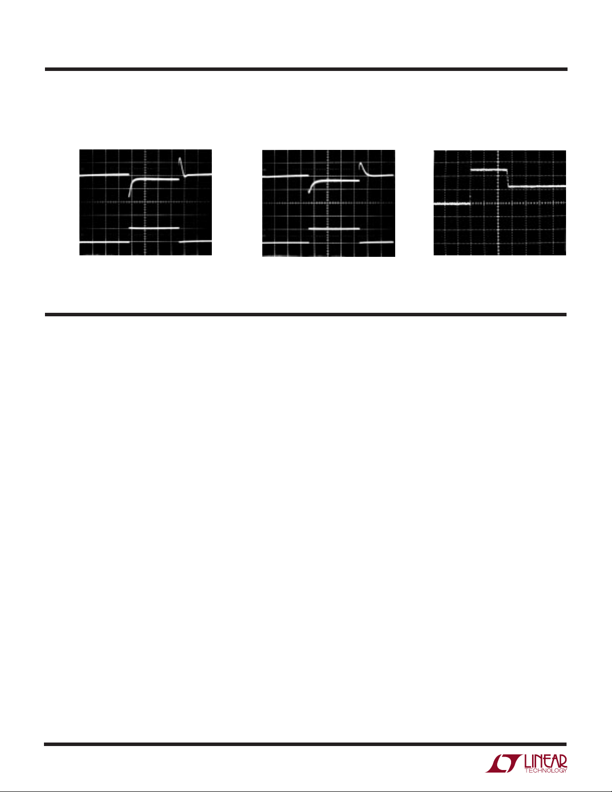
LTC1695
1695 • G23
V
OUT
2V/DIV
100ms/DIV
V
CC
= 5V
C
IN
= 10µF
C
OUT
= 4.7µF
I
LOAD
= 1mA
UW
TYPICAL PERFOR A CE CHARACTERISTICS
V
(AC)
OUT
20mV/DIV
I
LOAD
50mA/DIV
Load Transient Response
Dropout (Code 63), 5mA to 55mA
V
= 5V
CC
= 4.7µF TANTALUM
C
OUT
100µs/DIV
1695 • G21
V
20mV/DIV
50mA/DIV
Load Transient Response
Dropout (Code 63), 50mA to 100mA
(AC)
OUT
I
LOAD
V
= 5V
CC
= 4.7µF TANTALUM
C
OUT
UUU
PIN FUNCTIONS
VCC (Pin 1): Power Supply Input. VCC supplies current to
the internal control circuitry, serves as the reference for
the 6-bit DAC and acts as the power path for the P-channel
low dropout linear regulator. Bypass V
with a low ESR capacitor ≥10µF.
GND (Pin 2): Ground. Tie GND to the ground plane.
SCL (Pin 3): SMBus Clock Input. Data is shifted into SDA
on the rising edge of the SCL clock signal during data
transfer.
directly to ground
CC
Boost Start Timer
100µs/DIV
1695 • G22
SDA (Pin 4): SMBus Bidirectional Data Input/Digital Output. SDA is an open drain output and requires a pull-up
resistor or current source to VCC. Data is shifted into SDA
and acknowledged by SDA.
V
(Pin 5): Linear Regulator Output. Connect directly to
OUT
the fan’s +VE terminal. V
is set to VZS (code 0) on
OUT
power-up. For good transient response and stability, use
a general purpose, low cost, medium ESR (0.1Ω to 1Ω)
tantalum or electrolytic capacitor. LTC recommends a
surface mount tantalum capacitor of ≥4.7µF.
6
 Loading...