

Linear Technology LTC1694-1 Datasheet
FEATURES
■
Improves SMBus/I2CTM Rise Time Transition
■
Ensures Data Integrity with Multiple Devices
on the SMBus/I2C
■
Improves Low State Noise Margin
■
Wide Supply Voltage Range: 2.7V to 6V
■
Tiny 5-Pin SOT-23 Package
■
Parallel Multiple LTC1694-1 Devices
for Increased Drive
U
APPLICATIO S
■
Notebook and Palmtop Computers
■
Portable Instruments
■
Battery Chargers
■
Industrial Control Application
■
TV/Video Products
■
ACPI SMBus Interface
LTC1694-1
SMBus/I2C Accelerator
U
DESCRIPTIO
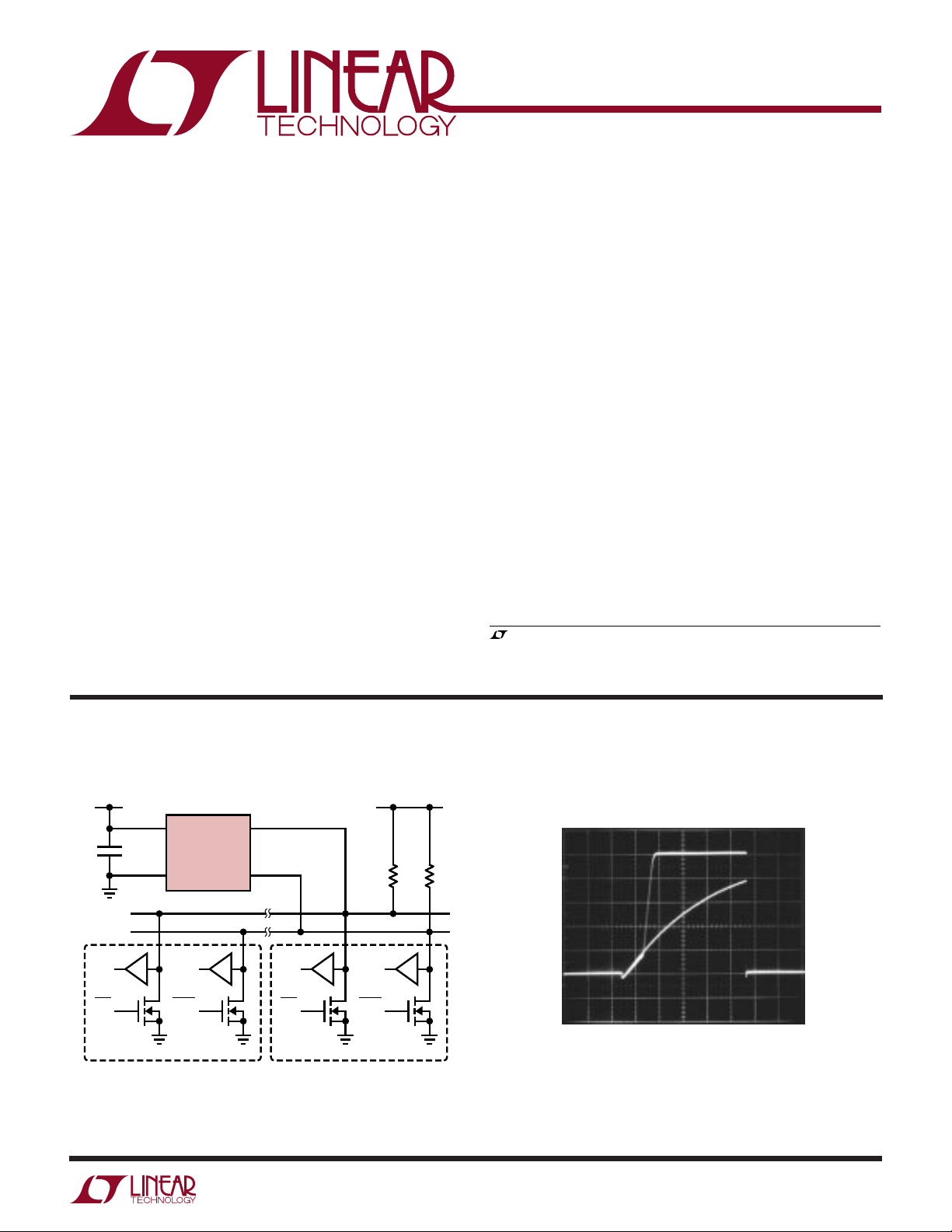
The LTC®1694-1 is a dual SMBus active pull-up designed
to enhance data transmission speed and reliability under
all specified SMBus loading conditions. The LTC1694-1 is
also compatible with the Philips I2C Bus.
The LTC1694-1 allows multiple device connections or a
longer, more capacitive interconnect, without compromising slew rates or bus performance, by supplying a high
pull-up current of 2.2mA to slew the SMBus or I2C lines
during positive bus transitions
During negative transitions or steady DC levels, the
LTC1694-1 sources zero current. External resistors, one
on each bus line, trigger the LTC1694-1 during positive
bus transitions and set the pull-down current level. These
resistors determine the slew rate during negative bus
transitions and the logic low DC level.
The LTC1694-1 is available in a 5-pin SOT-23 package.
, LTC and LT are registered trademarks of Linear Technology Corporation.
I2C is a trademark of Philips Electronics N.V.
TYPICAL APPLICATIO
V
CC
5V
1
V
C1
0.1µF
2
GND
SCL
SMBus
SDA
CLK
IN
CLK
OUT
DEVICE 1
LTC1694-1: Patent Pending
DATA
DATA
CC
LTC1694-1
IN
OUT
SMBus1
SMBus2
5
4
CLK
IN
CLK
OUT
DEVICE N
U
V
CC
5V
DATA
DATA
OUT
Comparison of SMBus Waveforms for
the LTC1694-1 vs Resistor Pull-Up
R
R
P2
P1
IN
1694-1 TA01
LTC1694-1
1V/DIV
VCC = 5V 1µs/DIV 1694-1 TA02
CLD = 200pF
= 100kHz
f
SMBus
R
PULL-UP
= 15.8k
1
LTC1694-1
VCC 1
GND 2
NC 3
5 SMBus1
4 SMBus2
TOP VIEW
S5 PACKAGE
5-LEAD PLASTIC SOT-23
WW
W
ABSOLUTE MAXIMUM RATINGS
(Note 1)
Supply Voltage (VCC) ................................................. 7V
SMBus1, SMBus2 Inputs ............ –0.3V to (VCC + 0.3V)
Operating Ambient Temperature Range....... 0°C to 70°C
U
U
W
PACKAGE/ORDER INFORMATION
ORDER PART
NUMBER
LTC1694-1CS5
Junction Temperature........................................... 125°C
Storage Temperature Range ................. –65°C to 150°C
S5 PART MARKING
Lead Temperature (Soldering, 10 sec.).................300°C
T
= 125°C, θJA = 256°C/W
JMAX
Consult factory for Industrial and Military grade parts.
ELECTRICAL CHARACTERISTICS
temperature range, otherwise specifications are at TA = 25°C. VCC = 2.7V to 6V, unless otherwise noted.
SYMBOL PARAMETER CONDITIONS MIN TYP MAX UNITS
V
CC
I
CC
I
PULL-UP
V
THRES
SR
THRES
t
r
f
MAX
Supply Voltage Range 2.7 6 V
Supply Current SMBus1 = SMBus2 = V
Pull-Up Current Positive Transition on SMBus ( Figure 1) ● 1.0 2.2 mA
Input Threshold Voltage Slew Rate = 0.5V/µs (Figure 1) ● 0.4 0.65 0.9 V
Slew Rate Detector Threshold SMBus > V
SMBus Rise Time Bus Capacitance = 200pF (Note 2) ● 0.32 1.0 µs
Standard Mode I
SMBus Maximum Operating Frequency (Note 4) ● 100 kHz
2
C Bus Rise Time Bus Capacitance = 400pF (Note 3) ● 0.30 1.0 µs
The ● denotes specifications which apply over the full operating
CC
Slew Rate = 0.5V/µs, SMBus > V
THRES
THRES
● 15 45 80 µA
● 0.2 0.5 V/µs
LTHE
U
Note 1: Absolute Maximum Ratings are those values beyond which the life
of a device may be impaired.
Note 2: The rise time of an SMBus line is calculated from (V
0.15V) to (V
guaranteed by design and not tested. With a minimum initial slew rate of
0.5V/µs, a minimum pull-up current of 1mA and a maximum input
threshold voltage of 0.9V:
2
–
+ 0.15V) or 0.65V to 2.25V. This parameter is
IH(MIN)
Rise Time = [(0.9V – 0.65V)/0.5V/µs] + [(2.25V – 0.9V) • 200pF/1mA]
= 0.77µs
IL(MAX)
Note 3: The rise time of an I2C bus line is calculated from V
or 1.5V to 3V (with VCC = 5V). This parameter is guaranteed by
V
IH(MIN)
design and not tested. With a minimum boosted pull-up current of 1mA:
Rise Time = (3V – 1.5V) • 400pF/1mA = 0.6µs
Note 4: This parameter is guaranteed by design and not tested.
IL(MAX)
to
W
U
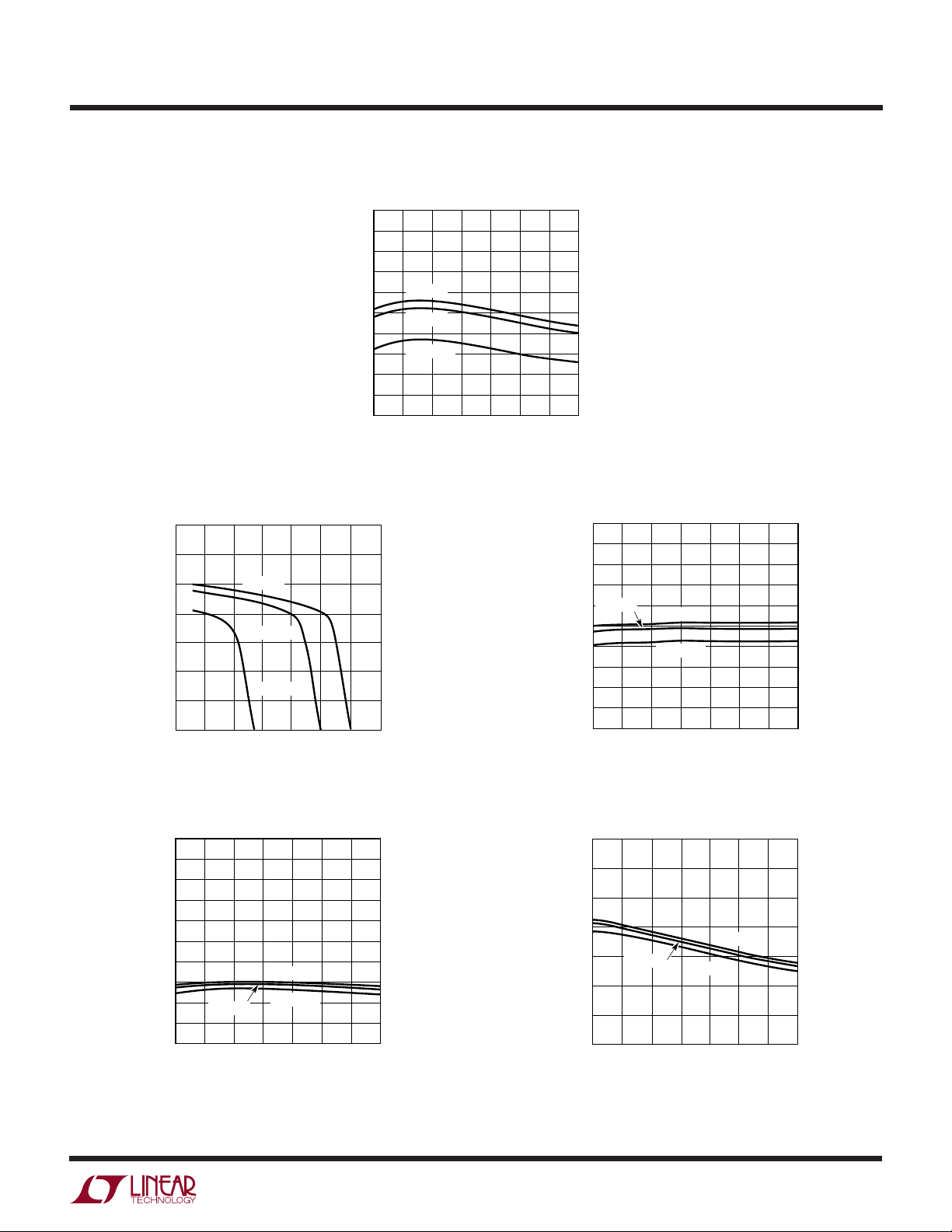
TYPICAL PERFORMANCE CHARACTERISTICS
Pull-Up Current
3.50
3.25
3.00
2.75
–50
VCC = 6V
VCC = 5V
VCC = 2.7V
0
–25
TEMPERATURE (°C)
50
25
75
100
1694-1 G01
Pull-Up Current
vs SMBus Voltage
3.5
3.0
2.5
2.0
1.5
1.0
PULL-UP CURRENT (mA)
0.5
0
0
12
SMBus VOLTAGE (V)
VCC = 6V
VCC = 5V
VCC = 2.7V
467
35
2.50
2.25
2.00
1.75
PULL-UP CURRENT (mA)
1.50
1.25
1.00
LT1694 G02
125
Input Threshold Voltage
0.90
0.85
0.80
0.75
VCC = 5V
0.70
0.65
0.60
0.55
0.50
INPUT THRESHOLD VOLTAGE (V)
0.45
0.40
–50
–25
VCC = 6V
VCC = 2.7V
0
25
TEMPERATURE (°C)
LTC1694-1
50
75
100
125
1694 G03
Slew Rate Detector Threshold
0.50
0.45
0.40
0.35
0.30
0.25
SLEW RATE DETECTOR THRESHOLD (V/µs)
0.20
0.15
0.10
0.05
0
–50
VCC = 5V
–25
VCC = 6V
VCC = 2.7V
0
TEMPERATURE (°C)
50
25
Standby Mode Supply Current
80
70
60
50
40
30
SUPPLY CURRENT (µA)
20
100
125
1694 G04
75
10
VCC = 5V
–25 25 75 125
–50
050
TEMPERATURE (°C)
VCC = 6V
VCC = 2.7V
100
1694-1 G05
3
 Loading...