

Linear Technology LTC1693 Datasheet
FEATURES
■
Dual MOSFET Drivers in SO-8 Package
or Single MOSFET Driver in MSOP Package
■
1GΩ Electrical Isolation Between the Dual Drivers
Permits High/Low Side Gate Drive
■
1.5A Peak Output Current
■
16ns Rise/Fall Times at VCC = 12V, CL = 1nF
■
Wide VCC Range: 4.5V to 13.2V
■
CMOS Compatible Inputs with Hysteresis,
Input Thresholds are Independent of V
■
Driver Input Can Be Driven Above V
■
Undervoltage Lockout
■
Thermal Shutdown
CC
CC
U
APPLICATIO S
■
Power Supplies
■
High/Low Side Drivers
■
Motor/Relay Control
■
Line Drivers
■
Charge Pumps
LTC1693
High Speed
Single/Dual MOSFET Drivers
U
DESCRIPTIO
The LTC®1693 family drives power MOSFETs at high
speed. The 1.5A peak output current reduces switching
losses in MOSFETs with high gate capacitance.
The LTC1693-1 contains two noninverting drivers. The
LTC1693-2 contains one noninverting and one inverting
driver. The LTC1693-1 and LTC1693-2 drivers are electrically isolated and independent. The LTC1693-3 is a single
driver with an output polarity select pin.
The LTC1693 has VCC independent CMOS input thresholds with 1.2V of typical hysteresis. The LTC1693 can
level-shift the input logic signal up or down to the rail-torail VCC drive for the external MOSFET.
The LTC1693 contains an undervoltage lockout circuit and
a thermal shutdown circuit. Both circuits disable the
external N-channel MOSFET gate drive when activated.
The LTC1693-1 and LTC1693-2 come in an 8-lead SO package. The LTC1693-3 comes in an 8-lead MSOP package.
, LTC and LT are registered trademarks of Linear Technology Corporation.
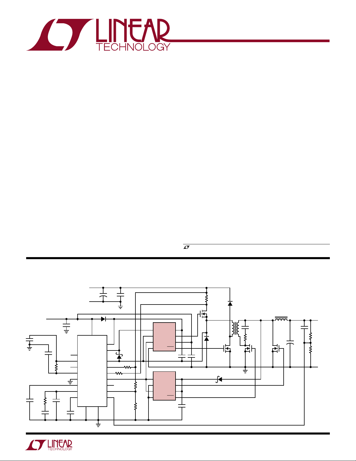
TYPICAL APPLICATIO
V
IN
C11
0.1µF
1800pF
C10
0.1µF
C14
3300pF
NPO
48VDC
±10%
RETURN
12V
C9
5%
R9
12k
R5
2.49k
1%
C12
100pF
C5
1µF
10
1
2
4
3
5
6
7
C15
0.1µF
SYNC
5V
REF
SL/ADJ
C
T
I
AVG
SS
V
C
V
REF
12V
LT1339
8
+
MURS120
17
IN
BOOST
SENSE
SENSE
PHASE
RUN/SHDN
PGNDSGND
15
C1
330µF
63V
D2
TG
TS
+
–
BG
V
FB
20
19
18
11
12
16
14
13
9
U
R7 100Ω
C2
1.5µF
63V
BAT54
R6 100Ω
Two Transistor Foward Converter
LTC1693CS8-2
R8
301k
1%
R10
10k
1%
1
IN1
2
GND1
3
IN2
4
GND2
LTC1693CS8-2
1
IN1
2
GND1
3
IN2
4
GND2
V
OUT1
V
OUT2
V
OUT1
V
OUT2
8
CC1
7
6
CC2
5
C7
1µF
8
CC1
7
6
CC2
5
C13
1µF
C8
1µF
R1
0.068Ω
Q1
MTD20NO6HD
D1
MURS120
T1
13:2
••
D3
MURS120
Si4420
Q3
MTD20NO6HD
D4
MBRO530T1
C1: SANYO 63MV330GX
C2: WIMA SMD4036/1.5/63/20/TR
C6: KEMET T510X477M006AS (×8)
L1: GOWANDA 50-318
T1: GOWANDA 50-319
L1
1.5µH
C3
4700pF
25V
R2
5.1Ω
Q4
Si4420
Q2
×2
C4
0.1µF
C6
+
470µF
6.3V
×8
1693 TA01
R3
249Ω
1%
R4
1.24k
1%
V
OUT
1.5V/15A
RETURN
1
LTC1693
WW
W
U
ABSOLUTE MAXIMUM RATINGS
(Note 1)
Supply Voltage (VCC) .............................................. 14V
Inputs (IN, PHASE)................................... –0.3V to 14V
Driver Output................................. –0.3V to VCC + 0.3V
GND1 to GND2 (Note 5) ..................................... ±100V
U
W
U
PACKAGE/ORDER INFORMATION
TOP VIEW
IN1
IN1
1
GND1
2
IN2
3
GND2
4
S8 PACKAGE
8-LEAD PLASTIC SO
T
= 150°C, θJA = 135°C/W
JMAX
ORDER PART
NUMBER
V
8
CC1
OUT1
7
V
6
CC2
OUT2
5
S8 PART
MARKING
ORDER PART
NUMBER
1
GND1
2
IN2
3
GND2
4
8-LEAD PLASTIC SO
T
= 150°C, θJA = 135°C/W
JMAX
S8 PACKAGE
Junction Temperature.......................................... 150°C
Operating Ambient Temperature Range.......0°C to 70°C
Storage Temperature Range................. –65°C to 150 °C
Lead Temperature (Soldering, 10 sec)..................300°C
TOP VIEW
V
8
CC1
OUT1
7
V
6
CC2
OUT2
5
S8 PART
MARKING
PHASE
GND
ORDER PART
NUMBER
TOP VIEW
IN
1
NC
2
3
4
MS8 PACKAGE
8-LEAD PLASTIC MSOP
T
= 150°C, θJA = 200°C/W
JMAX
8
7
6
5
MS8 PART
MARKING
V
CC
OUT
NC
NC
LTC1693-1CS8 16931
Consult factory for Industrial and Military grade parts.
LTC1693-2CS8
ELECTRICAL CHARACTERISTICS
The ● denotes specifications which apply over the full operating
16932
LTC1693-3CMS8 LTEB
temperature range, otherwise specifications are at TA = 25°C. VCC = 12V, unless otherwise noted.
SYMBOL PARAMETER CONDITIONS MIN TYP MAX UNITS
V
CC
I
CC
I
CC(SW)
Input
V
IH
V
IL
I
IN
V
PH
I
PH
Output
V
OH
V
OL
R
ONL
R
ONH
I
PKL
I
PKH
Supply Voltage Range 4.5 13.2 V
Quiescent Current LTC1693-1, LTC1693-2, IN1 = IN2 = 0V (Note 2) ● 400 720 1100 µA
LTC1693-3, PHASE = 12V, IN = 0V
Switching Supply Current LTC1693-1, LTC1693-2, C
LTC1693-3, C
High Input Threshold ● 2.2 2.6 3.1 V
Low Input Threshold ● 1.1 1.4 1.7 V
Input Pin Bias Current ● ±0.01 ±10 µA
PHASE Pin High Input Threshold (Note 3) ● 4.5 5.5 6.5 V
PHASE Pin Pull-Up Current PHASE = 0V (Note 3) ● 10 20 45 µA
High Output Voltage I
Low Output Voltage I
Output Pull-Down Resistance 2.85 Ω
Output Pull-Up Resistance 3.00 Ω
Output Low Peak Current 1.70 A
Output High Peak Current 1.40 A
= –10mA ● 11.92 11.97 V
OUT
= 10mA ● 30 75 mV
OUT
= 4.7nF, fIN = 100kHz ● 7.2 10 mA
OUT
= 4.7nF, fIN = 100kHz ● 14.4 20 mA
OUT
● 200 360 550 µA
2
LTC1693
ELECTRICAL CHARACTERISTICS
The ● denotes specifications which apply over the full operating
temperature range, otherwise specifications are at TA = 25°C. VCC = 12V, unless otherwise noted.
SYMBOL PARAMETER CONDITIONS MIN TYP MAX UNITS
Switching Timing (Note 4)
t
RISE
t
FALL
t
PLH
t
PHL
Output Rise Time C
Output Fall Time C
Output Low-High Propagation Delay C
Output High-Low Propagation Delay C
= 1nF ● 17.5 35 ns
OUT
C
= 4.7nF ● 48.0 85 ns
OUT
= 1nF ● 16.5 35 ns
OUT
C
= 4.7nF ● 42.0 75 ns
OUT
= 1nF ● 38.0 70 ns
OUT
= 4.7nF ● 40.0 75 ns
C
OUT
= 1nF ● 32 70 ns
OUT
= 4.7nF ● 35 75 ns
C
OUT
Driver Isolation
R
ISO
Note 1: Absolute Maximum Ratings are those values beyond which the life
of a device may be impaired.
Note 2: Supply current is the total current for both drivers.
GND1-GND2 Isolation Resistance LTC1693-1, LTC1693-2 GND1-to-GND2 Voltage = 75V ● 0.075 1 GΩ
Note 4: All AC timing specificatons are guaranteed by design and are not
production tested.
Note 5: Only applies to the LTC1693-1 and LTC1693-2.
Note 3: Only the LTC1693-3 has a PHASE pin.
UW
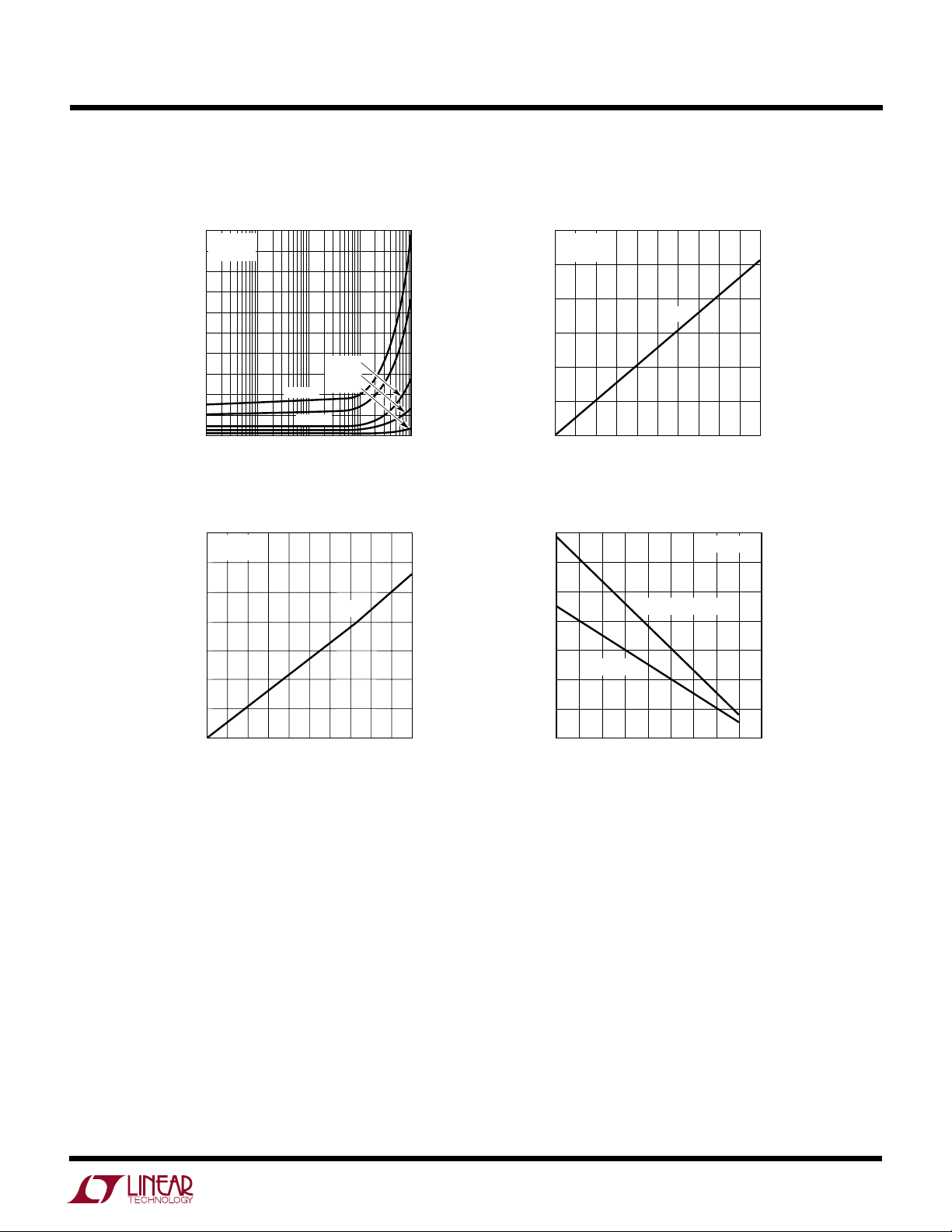
TYPICAL PERFOR A CE CHARACTERISTICS
IN Threshold Voltage vs V
2.75
TA = 25°C
2.50
2.25
2.00
1.75
1.50
INPUT THRESHOLD VOLTAGE (V)
1.25
1.00
5
67
V
IL
810
VCC (V)
CC
V
IH
91112
1693 G01
IN Threshold Voltage
vs Temperature
3.00
VCC = 12V
2.75
2.50
2.25
2.00
1.75
1.50
INPUT THRESHOLD VOLTAGE (V)
1.25
1.00
–25 0 50
–50
25
TEMPERATURE (°C)
V
IH
V
IL
75 100 125
1693 G02
IN Threshold Hysteresis
vs Temperature
1.4
VCC = 12V
1.3
1.2
V
IH-VIL
1.1
1.0
0.9
INPUT THRESHOLD HYSTERESIS (V)
0.8
–25 0 50 100 125
–50
25 75
TEMPERATURE (°C)
1693 G03
3
LTC1693
UW
TYPICAL PERFOR A CE CHARACTERISTICS
PHASE Threshold Voltage vs V
6
TA = 25°C
5
V
4
3
2
1
PHASE THRESHOLD VOLTAGE (V)
0
5
67
Rise/Fall Time vs C
120
TA = 25°C
= 12V
V
CC
= 100kHz
f
100
IN
80
60
TIME (ns)
40
20
0
1 100 1000 10000
PH(H)
810
VCC (V)
10
(pF)
C
OUT
V
91112
OUT
t
RISE
PH(L)
t
FALL
CC
1693 G04
1693 G07
Rise/Fall Time vs V
24
22
20
18
16
TIME (ns)
14
12
10
5
67
55
50
45
40
35
30
TIME (ns)
25
20
15
10
t
PHL
6891110 12
5
CC
t
RISE
t
FALL
91112
810
VCC (V)
t
PLH
7
VCC (V)
TA = 25°C
C
OUT
= 100kHz
f
IN
CC
TA = 25°C
C
OUT
= 100kHz
f
IN
= 1nF
1693 G05
= 1nF
1693 G08
Rise/Fall Time vs Temperature
20
VCC = 12V
19
C
= 1nF
18
17
16
15
TIME (ns)
14
13
12
11
10
–50
OUT
= 100kHz
f
IN
–25
0
TEMPERATURE (°C)
t
RISE
50
25
Propagation Delay vs TemperaturePropagation Delay vs V
50
VCC = 12V
= 1nF
C
OUT
= 100kHz
45
f
IN
40
t
–50
PLH
–25 0
t
PHL
50
25 75
TEMPERATURE (°C)
35
TIME (ns)
30
25
20
t
FALL
75
125
100
1693 G06
100 125
1693 G09
Propagation Delay vs C
50
TA = 25°C
= 12V
V
CC
= 100kHz
f
IN
40
t
PLH
TIME (ns)
30
20
1 100 1000 10000
t
PHL
10
C
(pF)
OUT
4
OUT
1693 G10
Output Saturation Voltage
vs Temperature
200
VCC = 12V
150
100
50
OUTPUT SATURATION VOLTAGE (mV)
0
–55
VOH (50mA) wrt V
VOH (10mA) wrt V
VOL (10mA)
–35 –15 5 25
TEMPERATURE (°C)
CC
VOL (50mA)
CC
45 65 85 105 125
1693 G11
Quiescent Current
vs VCC (Single Driver)
350
TA = 25°C
= 0V
V
IN
300
250
200
QUIESCENT CURRENT (µA)
150
100
56
7
8
VCC (V)
9
10
11
12
1693 G12
UW
TYPICAL PERFOR A CE CHARACTERISTICS
Switching Supply Current
vs C
(Single Driver)
OUT
100
TA = 25°C
90
V
= 12V
CC
80
70
60
50
40
30
20
SWITCHING SUPPLY CURRENT (mA)
10
0
1 100 1000 10000
10
750kHz
500kHz
C
OUT
200kHz
100kHz
25kHz
(pF)
1693 G13
300
250
200
150
(mV)
OL
V
100
50
0
VOL vs Output Current
VCC = 12V
= 25°C
T
A
V
OL
20 40 60 80
OUTPUT CURRENT (mA)
LTC1693
10010030507090
1693 G14
VOH vs Output Current
350
TA = 25°C
= 12V
V
CC
300
250
200
(mV)
OH
150
V
100
50
0
0
30
20
10
OUTPUT CURRENT (mA)
40
50
60 80
Thermal Derating Curves
1400
1200
1000
V
OH
90
1693 G15
100
70
800
600
400
POWER DISSIPATION (mW)
200
LTC1693-3
0
–35 –15 5 25 45 125
–55
LTC1693-1/LTC1693-2
AMBIENT TEMPERATURE (°C)
TJ = 125°C
65 85 105
1693 G16
5
LTC1693
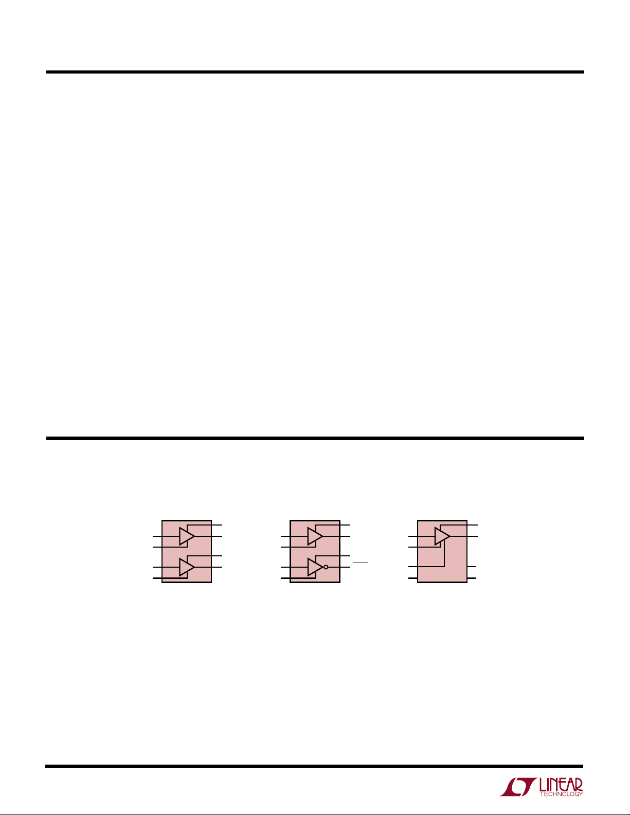
UUU
PIN FUNCTIONS
SO-8 Package (LTC1693-1, LTC1693-2)
IN1, IN2 (Pins 1, 3):
Driver Inputs. The inputs have V
CC
independent thresholds with 1.2V typical hysteresis to
improve noise immunity.
GND1, GND2 (Pins 2, 4): Driver Grounds. Connect to a
low impedance ground. The VCC bypass capacitor should
connect directly to this pin. The source of the external
MOSFET should also connect directly to the ground pin.
This minimizes the AC current path and improves signal
integrity. The ground pins should not be tied together if
isolation is required between the two drivers of the
LTC1693-1 and the LTC1693-2.
OUT 1, OUT2 (Pins 5, 7): Driver Outputs. The LTC16931’s outputs are in phase with their respective inputs (IN1,
IN2). The LTC1693-2’s topside driver output (OUT1) is in
phase with its input (IN1) and the bottom side driver’s
output (OUT2) is opposite in phase with respect to its input
pin (IN2).
V
, V
CC1
(Pins 6, 8): Power Supply Inputs.
CC2
MSOP Package (LTC1693-3)
IN (Pin 1):
Driver Input. The input has VCC independent
thresholds with hysteresis to improve noise immunity.
NC (Pins 2, 5, 6): No Connect.
PHASE (Pin 3): Output Polarity Select. Connect this pin to
VCC or leave it floating for noninverting operation. Ground
this pin for inverting operation. The typical PHASE pin
input current when pulled low is 20µA.
GND (Pin 4): Driver Ground. Connect to a low impedance
ground. The VCC bypass capacitor should connect directly
to this pin. The source of the external MOSFET should also
connect directly to the ground pin. This minimizes the AC
current path and improves signal integrity.
OUT (Pin 7): Driver Output.
VCC (Pin 8): Power Supply Input.
W
BLOCK DIAGRA SM
1
IN1
2
GND1
3
IN2
4
GND2
LTC1693-1
DUAL NONINVERTING DRIVER
8
V
CC1
7
OUT1
6
V
CC2
5
OUT2
1
IN1
2
GND1
3
IN2
4
GND2
TOPSIDE NONINVERTING DRIVER
AND BOTTOM SIDE INVERTING DRIVER
LTC1693-2
8
V
CC1
7
OUT1
6
V
CC2
5
OUT2
1
IN
4
GND
3
PHASE
2
NC
SINGLE DRIVER WITH
POLARITY SELECT
LTC1693-3
8
V
CC
7
OUT
6
NC
5
NC
1693 BD
6
 Loading...