

Linear Technology LTC1690 Datasheet
FEATURES
LTC1690
Differential Driver and
Receiver Pair with Fail-Safe
Receiver Output
U
DESCRIPTIO
■
No Damage or Latchup to ±15kV ESD (Human Body
Model), IEC1000-4-2 Level 4 (±8kV) Contact and
Level 3 (±8kV) Air Discharge
■
Guaranteed High Receiver Output State for
Floating, Shorted or Terminated Inputs with No
Signal Present
■
Drives Low Cost Residential Telephone Wires
■
ICC = 600µA Max with No Load
■
Single 5V Supply
■
–7V to 12V Common Mode Range Permits ±7V
Ground Difference Between Devices on the Data Line
■
Power-Up/Down Glitch-Free Driver Outputs Permit
Live Insertion or Removal of Transceiver
■
Driver Maintains High Impedance with the Power Off
■
Up to 32 Transceivers on the Bus
■
Pin Compatible with the SN75179 and LTC490
■
Available in SO, MSOP and PDIP Packages
U
APPLICATIO S
■
Battery-Powered RS485/RS422 Applications
■
Low Power RS485/RS422 Transceiver
■
Level Translator
■
Line Repeater
The LTC®1690 is a low power receiver/driver pair that is
compatible with the requirements of RS485 and RS422.
The receiver offers a fail-safe feature that guarantees a
high receiver output state when the inputs are left open,
shorted together or terminated with no signal present. No
external components are required to ensure the high
receiver output state.
Separate driver output and receiver input pins allow full
duplex operation. Excessive power dissipation caused by
bus contention or faults is prevented by a thermal shutdown circuit which forces the driver outputs into a high
impedance state.
The LTC1690 is fully specified over the commercial and
industrial temperature ranges. The LTC1690 is available in
8-Pin SO, MSOP and PDIP packages.
, LTC and LT are registered trademarks of Linear Technology Corporation.
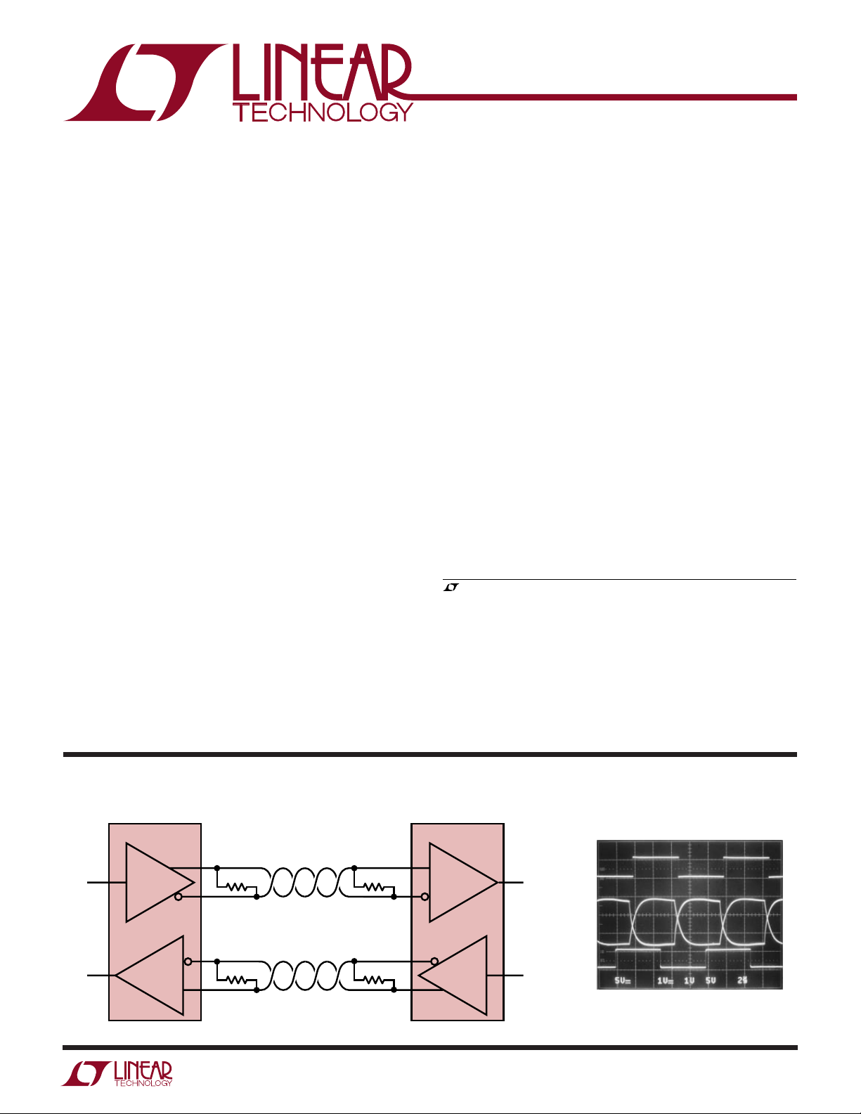
TYPICAL APPLICATIO
LTC1690 LTC1690
5
Y1
3
D1
2
R1
120Ω
6
Z1
7
B1
120Ω
8
A1
U
120Ω
120Ω
Driving a 1000 Foot STP Cable
8
A2
2
RECEIVER
7
B2
Z2
6
5
Y2
1690 TA01
R2DRIVER
3
D2RECEIVER DRIVER
D1
B2
A2
R2
1690 TA01a
1
LTC1690
1
2
3
4
8
7
6
5
TOP VIEW
MS8 PACKAGE
8-LEAD PLASTIC MSOP
V
CC
R
D
GND
A
B
Z
Y
WW
W
ABSOLUTE MAXIMUM RATINGS
U
(Note 1)
Supply Voltage (VCC) .............................................. 6.5V
Driver Input Voltage..................... –0.3V to (VCC + 0.3V)
Driver Output Voltages ................................. –7V to 10V
Receiver Input Voltages ......................................... ±14V
Receiver Output Voltage .............. –0.3V to (VCC + 0.3V)
Junction Temperature........................................... 125°C
U
W
PACKAGE/ORDER INFORMATION
ORDER PART
NUMBER
LTC1690CMS8
T
JMAX
= 125°C, θ
= 200°C/W
JA
MS8 PART MARKING
LTDA
Operating Temperature Range
LTC1690C ........................................ 0°C ≤ TA ≤ 70°C
LTC1690I..................................... – 40°C ≤ TA ≤ 85°C
Storage Temperature Range ................. –65°C to 150°C
Lead Temperature (Soldering, 10 sec).................. 300°C
U
ORDER PART
V
1
CC
R
2
D
3
GND
4
S8 PACKAGE
8-LEAD PLASTIC SO
T
= 125°C, θ
JMAX
= 125°C, θ
T
JMAX
TOP VIEW
R
D
N8 PACKAGE
8-LEAD PLASTIC DIP
= 130°C/W (N)
JA
= 135°C/W (S)
JA
A
8
B
7
Z
6
Y
5
NUMBER
LTC1690CN8
LTC1690IN8
LTC1690CS8
LTC1690IS8
S8 PART MARKING
1690
1690I
DC ELECTRICAL CHARACTERISTICS
Consult factory for Military Grade Parts
The ● denotes the specifications which apply over the full operating
temperature range, otherwise specifications are at T
SYMBOL PARAMETER CONDITIONS MIN TYP MAX UNITS
V
OD1
V
OD2
V
OD3
∆V
V
OC
∆|VOC| Change in Magnitude of Driver Common Mode R = 22Ω, 27Ω or 50Ω, Figure 1 ● 0.2 V
V
IH
V
IL
I
IN1
I
IN2
V
TH
∆V
2
Differential Driver Output Voltage (Unloaded) IO = 0 ● V
Differential Driver Output Voltage (with Load) R = 50Ω; (RS422) ● 2V
Differential Driver Output Voltage (with Common Mode) V
Change in Magnitude of Driver Differential Output R = 22Ω, 27Ω or 50Ω, Figure 1 ● 0.2 V
OD
Voltage for Complementary Output States V
Driver Common Mode Output Voltage R = 22Ω, 27Ω or 50Ω, Figure 1 ● 3V
Output Voltage for Complementary Output States
Input High Voltage Driver Input (D) ● 2V
Input Low Voltage Driver Input (D) ● 0.8 V
Input Current Driver Input (D) ● ±2 µA
Input Current (A, B) VCC = 0V or 5.25V, VIN = 12V ● 1mA
Differential Input Threshold Voltage for Receiver –7V ≤ VCM ≤ 12V ● –0.20 –0.01 V
Receiver Input Hysteresis VCM = 0V ±30 mV
TH
= 25°C. VCC = 5V ±5% (Notes 2, 3)
A
R = 22Ω or 27Ω; (RS485), Figure 1
= –7V to 12V, Figure 2 1.5 5 V
TST
= –7V to 12V, Figure 2
TST
= 0V or 5.25V, VIN = –7V ● –0.8 mA
V
CC
CC
● 1.5 5 V
V
LTC1690
DC ELECTRICAL CHARACTERISTICS
temperature range, otherwise specifications are at T
= 25°C. VCC = 5V ±5% (Notes 2, 3)
A
The ● denotes the specifications which apply over the full operating
SYMBOL PARAMETER CONDITIONS MIN TYP MAX UNITS
V
OH
V
OL
R
IN
I
CC
I
OSD1
I
OSD2
I
OZ
I
OSR
t
PLH
t
PHL
t
SKEW
tr, t
t
PLH
t
PHL
t
SKD
f
MAX
Note 1: Absolute Maximum Ratings are those values beyond which the life
of the device may be impaired.
Receiver Output High Voltage IO = –4mA, VID = 200mV ● 3.5 V
Receiver Output Low Voltage IO = 4mA, VID = –200mV ● 0.4 V
Receiver Input Resistance –7V ≤ VCM ≤ 12V ● 12 22 kΩ
Supply Current No Load ● 260 600 µA
Driver Short-Circuit Current, V
Driver Short-Circuit Current, V
= HIGH –7V ≤ VO ≤ 10V 35 250 mA
OUT
= LOW –7V ≤ VO ≤ 10V 35 250 mA
OUT
Driver Three-State Current (Y, Z) –7V ≤ VO ≤ 10V, VCC = 0V ● 5 200 µA
Receiver Short-Circuit Current 0V ≤ VO ≤ V
Driver Input to Output, Figure 3, Figure 4 R
Driver Input to Output, Figure 3, Figure 4 R
Driver Output to Output, Figure 3, Figure 4 R
Driver Rise or Fall Time, Figure 3, Figure 4 R
f
Receiver Input to Output, Figure 3, Figure 5 R
Receiver Input to Output, Figure 3, Figure 5 R
|t
– t
PLH
|, Differential Receiver Skew, Figure 3, Figure 5 R
PHL
Maximum Data Rate, Figure 3, Figure 5 R
CC
= 54Ω, CL1 = CL2 = 100pF ● 10 22.5 60 ns
DIFF
= 54Ω, CL1 = CL2 = 100pF ● 10 25 60 ns
DIFF
= 54Ω, CL1 = CL2 = 100pF ● 2.5 15 ns
DIFF
= 54Ω, CL1 = CL2 = 100pF ● 21340 ns
DIFF
= 54Ω, CL1 = CL2 = 100pF ● 30 94 160 ns
DIFF
= 54Ω, CL1 = CL2 = 100pF ● 30 89 160 ns
DIFF
= 54Ω, CL1 = CL2 = 100pF 5 ns
DIFF
= 54Ω, CL1 = CL2 = 100pF ● 5 Mbps
DIFF
● 785mA
Note 2: All currents into device pins are positive; all currents out of device
pins are negative. All voltages are referenced to device ground unless
otherwise specified.
Note 3: All typicals are given for V
= 5V and TA = 25°C.
CC
UW
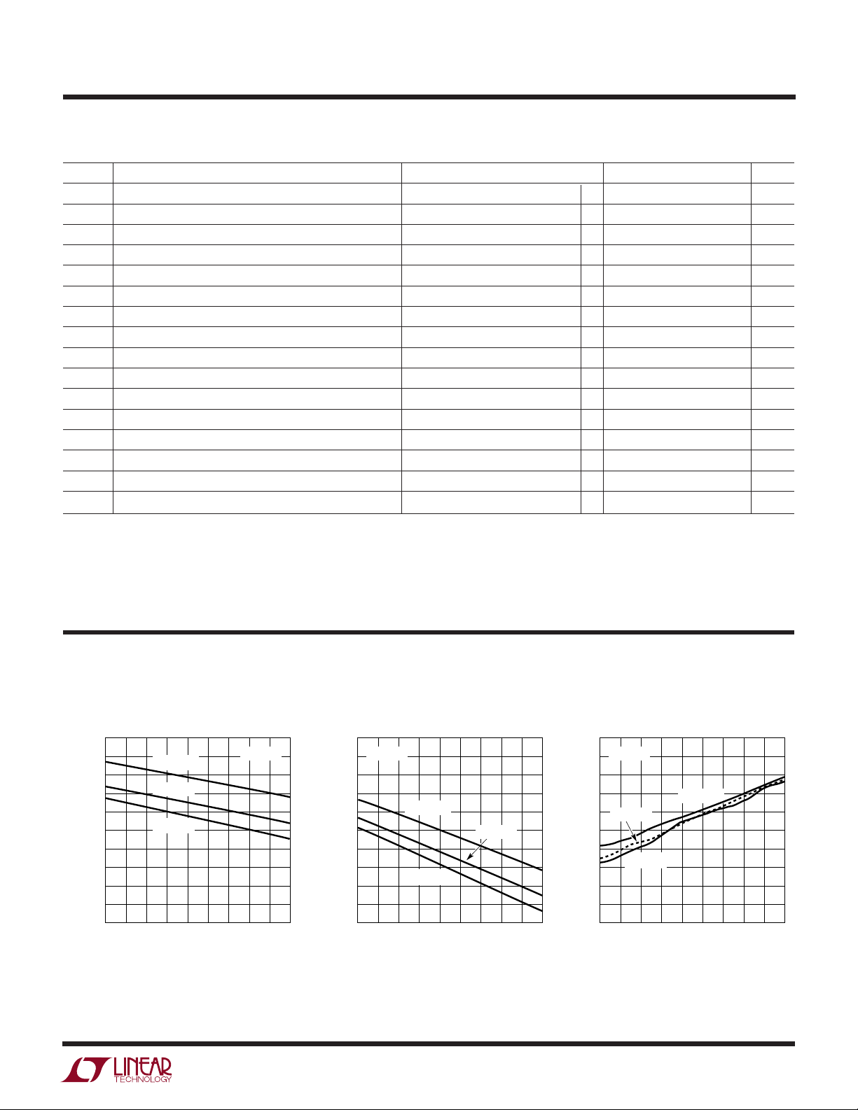
TYPICAL PERFOR A CE CHARACTERISTICS
Receiver Input Threshold Voltage
(Output High) vs Temperature
0
–20
–40
–60
–80
–100
–120
–140
–160
–180
RECEIVER INPUT THRESHOLD VOLTAGE (mV)
–200
–55 –35 –15 5 25 45 65 85 105 125
VCM = 12V
VCM = 0V
VCM = –7V
TEMPERATURE (°C)
VCC = 5V
1690 G01
Receiver Input Threshold Voltage
(Output Low) vs Temperature
0
VCC = 5V
–20
–40
–60
–80
–100
–120
–140
–160
–180
RECEIVER INPUT THRESHOLD VOLTAGE (mV)
–200
–55 –35 –15 5 25 45 65 85 105 125
VCM = 12V
VCM = 0V
VCM = –7V
TEMPERATURE (°C)
1690 G02
Receiver Hysteresis vs
Temperature
100
VCC = 5V
90
80
70
60
VCM = 0V
50
40
30
20
RECEIVER HYSTERESIS (mV)
10
VCM = –7V
0
–55 –35 –15 5 25 45 65 85 105 125
VCM = 12V
TEMPERATURE (°C)
1690 G03
3
LTC1690
UW
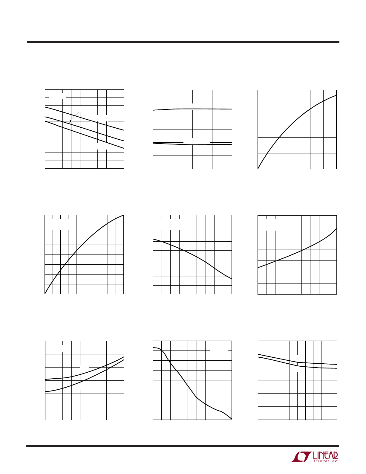
TYPICAL PERFOR A CE CHARACTERISTICS
Receiver Input Offset Voltage vs
Temperature
0
VCC = 5V
–20
–40
–60
–80
–100
–120
–140
–160
–180
RECEIVER INPUT OFFSET VOLTAGE (mV)
–200
–55 –35 –15 5 25 45 65 85 105 125
VCM = 0V
VCM = –7V
VCM = 12V
TEMPERATURE (°C)
Receiver Output Low Voltage vs
Output Current
40
TA = 25°C
35
= 4.75V
V
CC
30
25
20
15
10
RECEIVER OUTPUT CURRENT (mA)
5
0
0 0.2 0.4 0.6 0.8 1 1.2 1.4 1.6 1.8 2
RECEIVER OUTPUT LOW VOLTAGE (V)
1690 G04
1690 G07
Receiver Input Threshold Voltage
vs Supply Voltage
–40
TA = 25°C
–60
–80
–100
–120
–140
RECEIVER INPUT THRESHOLD VOLTAGE (mV)
–160
4.5 4.75 5 5.25 5.5
OUTPUT HIGH
OUTPUT LOW
SUPPLY VOLTAGE (V)
Receiver Output High Voltage vs
Temperature
4.8
I = 8mA
4.6
V
= 4.75V
CC
4.4
4.2
4.0
3.8
3.6
3.4
3.2
RECEIVER OUTPUT HIGH VOLTAGE (V)
3.0
–55 –35 –15 5 25 45 65 85 105 125
TEMPERATURE (°C)
1690 G05
1690 G08
Receiver Output High Voltage vs
Output Current
–25
TA = 25°C
V
= 4.75V
CC
–20
–15
–10
–5
RECEIVER OUTPUT CURRENT (mA)
0
4.5 4 3
5
RECEIVER OUTPUT HIGH VOLTAGE (V)
3.5
Receiver Output Low Voltage vs
Temperature
0.7
I = 8mA
= 4.75V
V
0.6
CC
0.5
0.4
0.3
0.2
0.1
RECEIVER OUTPUT LOW VOLTAGE (V)
0
–55 –35 –15 5 25 45 65 85 105 125
TEMPERATURE (°C)
2.5
2
1690 G06
1690 G09
Receiver Propagation Delay vs
Temperature
120
VCC = 5V
110
100
90
80
70
RECEIVER PROPAGATION DELAY (ns)
60
–55 –35 –15 5 25 45 65 85 105 125
t
PLH
t
PHL
TEMPERATURE (°C)
4
1690 G10
Receiver Skew t
PLH
– t
PHL
Temperature
10
9
8
7
6
5
RECEIVER SKEW (ns)
4
3
2
–55 –35 –15 5 25 45 65 85 105 125
TEMPERATURE (°C)
VCC = 5V
vs
1690 G11
Receiver Propagation Delay vs
Supply Voltage
110
100
90
80
70
60
RECEIVER PROPAGATION DELAY (ns)
50
4.5 4.6 4.7 4.8 4.9 5 5.1 5.2 5.3 5.4 5.5
t
PLH
t
PHL
SUPPLY VOLTAGE (V)
1690 G12
 Loading...