

Linear Technology LTC1687, LTC1686 Datasheet
FEATURES
■
Precision Propagation Delay Over Temperature:
Receiver/Driver: 18.5ns ±3.5ns
■
High Data Rate:
■
Low t
PLH/tPHL
52Mbps
Skew:
Receiver/Driver: 500ps Typ
■
–7V to 12V RS485 Input Common Mode Range
■
Guaranteed Fail-Safe Operation Over the Entire
Common Mode Range
■
High Input Resistance: ≥22k, Even When Unpowered
■
Short-Circuit Protected
■
Thermal Shutdown Protected
■
Driver Maintains High Impedance in Three-State or
with Power Off
■
Single 5V Supply
■
Pin Compatible with LTC490/LTC491
■
45dB CMRR at 26MHz
U
APPLICATIONS
■
High Speed RS485/RS422 Full Duplex Transceivers
■
Level Translator
■
Backplane Transceiver
■
STS-1/OC-1 Data Transceiver
■
Signal Repeaters
LTC1686/LTC1687
52Mbps Precision Delay
RS485 Fail-Safe Transceivers
U
DESCRIPTION
The LTC®1686/LTC1687 are high speed, precision delay,
full-duplex RS485 transceivers that can operate at data
rates as high as 52Mbps. The devices also meet the
requirements of RS422.
A unique architecture provides very stable propagation
delays and low skew over a wide common mode and
ambient temperature range.
The driver and receiver feature three-state outputs, with
disabled driver outputs maintaining high impedance over
the entire common mode range. A short-circuit feature
detects shorted outputs and substantially reduces driver
output current. A similar feature also protects the receiver
output from short circuits. Thermal shutdown circuitry
protects from excessive power dissipation.
The receiver has a fail-safe feature that guarantees a high
output state when the inputs are shorted or are left floating.
The LTC1686/LTC1687 RS485 transceivers guarantee
receiver fail-safe operation over the
range (–7V to 12V). Receiver input resistance remains
≥ 22k when the device is unpowered or disabled.
The LTC1686/LTC1687 operate from a single 5V supply
and draw only 7mA of supply current.
, LTC and LT are registered trademarks of Linear Technology Corporation.
entire
common mode
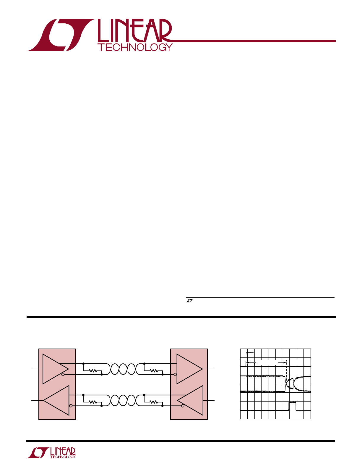
TYPICAL APPLICATION
LTC1686 LTC1686
3
D
R
DRIVER
2
RECEIVER
5
100Ω 100Ω
6
8
100Ω 100Ω
7
400 FT OF CATEGORY 5 UTP
U
RECEIVER
DRIVER
LTC1686/87 • TA01
10Mbps Data Pulse
400 Feet Category 5 UTP
1686/87 TA02
DRIVER INPUT
RECEIVER
INPUT
RECEIVER
OUTPUT
2V/DIV
R
1V/DIV
D
5V/DIV
CABLE DELAY
100ns/DIV
1
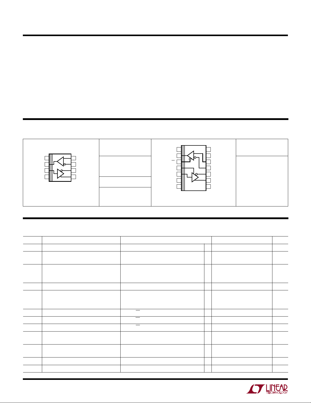
LTC1686/LTC1687
S8 PACKAGE
8-LEAD PLASTIC SO
1
2
3
4
8
7
6
5
TOP VIEW
V
DD
R
D
GND
A
B
Z
Y
R
D
A
W
O
LUTEXI T
S
A
WUW
ARB
U
G
I
S
(Note 1)
Supply Voltage (VDD).............................................. 10V
Control Input Currents .................... –100mA to 100mA
Control Input Voltages .................. –0.5V to VDD + 0.5V
Driver Input Voltages .................... –0.5V to VDD + 0.5V
Driver Output Voltages ................................. +12V/– 7V
Receiver Input Voltages ................................ +12V/–7V
Receiver Output Voltages ............. –0.5V to VDD + 0.5V
Receiver Input Differential ...................................... 10V
PACKAGE
/
O
RDER I FOR ATIO
WU
U
ORDER PART
NUMBER
LTC1686CS8
S8 PART MARKING
T
= 125°C, θ
JMAX
Consult factory for Industrial and Military grade parts.
= 150°C/ W
JA
1686
Driver Short-Circuit Duration
(V
: –7V to 10V)...................................... Indefinite
OUT
Receiver Short-Circuit Duration
(V
: 0V to VDD) ........................................ Indefinite
OUT
Operating Temperature Range .................... 0°C to 70°C
Storage Temperature Range ................ –65°C to 150°C
Lead Temperature (Soldering, 10 sec)................. 300°C
1
NC
2
R
3
RE
4
DE
5
D
6
GND
GND
14-LEAD PLASTIC SO
T
JMAX
TOP VIEW
R
S PACKAGE
= 125°C, θ
D
JA
14
13
12
11
10
9
87
= 90°C/W
V
DD
NC
A
B
Z
Y
NC
ORDER PART
NUMBER
LTC1687CS
DC ELECTRICAL CHARACTERISTICS
SYMBOL PARAMETER CONDITIONS MIN TYP MAX UNITS
V
OD1
V
OD2
∆V
OD
V
OC
∆VOC Change in Magnitude of Driver Common R = 27Ω or 50Ω, Figure 1 ● 0.2 V
V
IH
V
IL
I
IN1
I
IN2
V
TH
∆V
TH
V
OH
2
Differential Driver Output (Unloaded) I
Differential Driver Output (With Load) R = 50Ω (RS422) 2.0 V
Change in Magnitude of Driver Differential R = 27Ω or 50Ω, Figure 1 ● 0.2 V
Output Voltage for Complementary
Output States
Driver Common Mode Output Voltage R = 27Ω or 50Ω, VDD = 5V, Figure 1 ● 23V
Mode Output Voltage for Complementary
Output States
Input High Voltage D, DE, RE ● 2V
Input Low Voltage D, DE, RE ● 0.8 V
Input Current D, DE, RE ● –1 1 µA
Input Current (A, B) VA, VB = 12V, VDD = 0V or 5.25V ● 500 µA
Differential Input Threshold Voltage –7V ≤ VCM ≤ 12V ● –0.3 0.3 V
for Receiver
Receiver Input Hysteresis VCM = 0V 25 mV
Receiver Output High Voltage I
= 0 ● V
OUT
R = 27Ω (RS485), Figure 1 ● 1.5 V
, VB = –7V, VDD = 0V or 5.25V ● –500 µA
V
A
= –4mA, VID = 300mV ● 3.5 4.8 V
OUT
VDD = 5V ± 5% unless otherwise noted (Notes 2, 3).
DD
DD
V
V
LTC1686/LTC1687
DC ELECTRICAL CHARACTERISTICS
VDD = 5V ±5% unless otherwise noted (Notes 2, 3).
SYMBOL PARAMETER CONDITIONS MIN TYP MAX UNITS
V
I
OL
OZR
Receiver Output Low Voltage I
= 4mA, VID = –300mV ● 0.4 V
OUT
Three-State (High Impedance) Output 0.4V ≤ V
≤ 2.4V ● –1 1 µA
OUT
Current at Receiver
I
OZD
Three-State (High Impedance) Output V
= –7V to 12V ● –200 200 µA
OUT
Current at Driver
C
LOAD
I
DD
I
OSD1
I
OSD2
I
OSR
R
IN
C
IN
Receiver and Driver Output Load Capacitance (Note 4) ● 500 pF
Supply Current No Load, Pins D, DE, RE = 0V or V
Driver Short-Circuit Current, V
Driver Short-Circuit Current, V
Receiver Short-Circuit Current V
= HIGH V
OUT
= LOW V
OUT
= –7V or 10V (Note 5) ● 20 mA
OUT
= –7V or 10V (Note 5) ● 20 mA
OUT
OUT
= 0V or V
(Note 5) ● 20 mA
DD
● 712 mA
DD
Input Resistance –7V ≤ VCM ≤ 12V ● 22 kΩ
Input Capacitance A, B, D, DE, RE Inputs (Note 4) 3 pF
Open-Circuit Input Voltage VDD = 5V (Note 4), Figure 5 ● 3.2 3.3 3.4 V
Fail-Safe Time to Detect Fail-Safe Condition 2 µs
Time
CMRR Receiver Input Common Mode VCM = 2.5V, f = 26MHz 45 dB
Rejection Ratio
U
SWITCHING CHARACTERISTICS
SYMBOL PARAMETER CONDITIONS MIN TYP MAX UNITS
t
, t
PLH
t
SKEW
tr, t
f
t
ZH
t
ZL
t
LZ
t
HZ
t
PLH
t
SQD
t
ZL
t
ZH
t
LZ
t
HZ
t
PKG-PKG
Driver Input-to-Output Propagation Delay R
PHL
Figures 3, 5
Driver Output A-to-Output B Skew R
Figures 3, 5
Driver Rise/Fall Time R
Figures 3, 5
Driver Enable to Output High CL = 100pF, S2 Closed, Figures 4, 6 ● 25 50 ns
Driver Enable to Output Low CL = 100pF, S1 Closed, Figures 4, 6 ● 25 50 ns
Driver Disable from Low CL = 15pF, S1 Closed, Figures 4, 6 ● 25 50 ns
Driver Disable from High CL = 15pF, S2 Closed, Figures 4, 6 ● 25 50 ns
, t
Receiver Input-to-Output Propagation Delay CL = 15pF, Figures 3, 7 ● 15 18.5 22 ns
PHL
Receiver Skew t
PLH
– t
C
PHL
Receiver Enable to Output Low CL = 15pF, S1 Closed, Figures 2, 8 ● 25 50 ns
Receiver Enable to Output High CL = 15pF, S2 Closed, Figures 2, 8 ● 25 50 ns
Receiver Disable from Low CL = 15pF, S1 Closed, Figures 2, 8 ● 25 50 ns
Receiver Disable from High CL = 15pF, S2 Closed, Figures 2, 8 ● 25 50 ns
Maximum Receiver Input (Note 4) ● 2000 ns
Rise/Fall Times
Package-to-Package Skew CL = 15pF, Same Temperature (Note 4) 1.5 ns
Minimum Input Pulse Width VDD = 5V ±5% (Note 4) ● 17 19.2 ns
Maximum Data Rate VDD = 5V ±5% (Note 4) ● 52 60 Mbps
Maximum Input Frequency VDD = 5V ±5% (Note 4) ● 26 30 MHz
VDD = 5V, unless otherwise noted (Notes 2, 3).
= 54Ω, CL1 = CL2 = 100pF, ● 15 18.5 22 ns
DIFF
= 54Ω, CL1 = CL2 = 100pF, 500 ps
DIFF
= 54Ω, CL1 = CL2 = 100pF, 3.5 ns
DIFF
= 15pF, Figures 3, 7 500 ps
L
3
LTC1686/LTC1687
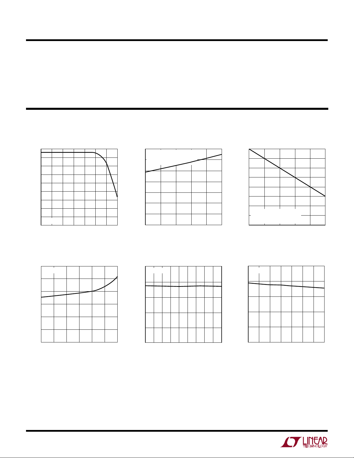
TEMPERATURE (°C)
–25
SUPPLY CURRENT (mA)
53
54
55
50
100
1686/87 G03
52
51
50
025 75
56
57
58
BOTH DRIVER AND RECEIVER
ENABLED AND LOADED
25Mbps DATA RATE
RECEIVER INPUT OVERDRIVE (V)
0.3 0.5
0
RECEIVER PROPAGATION DELAY (ns)
10
25
0.7
1.25
1.5
1686/87 G06
5
20
15
1.0
2.0
2.5
TA = 25°C
ELECTRICAL CHARACTERISTICS
The ● denotes specifications which apply over the full operating
temperature range.
Note 1: Absolute Maximum Ratings are those values beyond which the life
of a device may be impaired.
Note 2: All currents into the device pins are positive; all currents out of the
device pins are negative.
Note 3: All typicals are given for V
Note 4: Guaranteed by design, but not tested.
Note 5: Short-circuit current does not represent output drive capability.
When the output detects a short-circuit condition, output drive current is
significantly reduced (from hundreds of mA to 20mA max) until the short
is removed.
UW
TYPICAL PERFORMANCE CHARACTERISTICS
Receiver Input CMRR
46.5
46.0
45.5
45.0
44.5
44.0
43.5
43.0
42.5
COMMON MODE REJECTION RATIO (dB)
TA = 25°C
42.0
10
1k 100k 1M
FREQUENCY (Hz)
1686/87 G01
Supply Current vs Data Rate
70
BOTH DRIVER AND RECEIVER
ENABLED AND LOADED
60
= 25°C
T
A
50
40
30
20
SUPPLY CURRENT (mA)
10
0
10 20 50
1
DATA RATE (Mbps)
4030
1686/87 G02
= 5V, TA = 25°C.
DD
Supply Current vs Temperature
Receiver Propagation Delay
vs Load Capacitance
30
TA = 25°C
25
20
15
10
PROPAGATION DELAY (ns)
5
0
5
15
LOAD CAPACITANCE (pF)
4
25 35 55
105 205
1686/87 G04
Receiver Propagation Delay
vs Common Mode
25
TA = 25°C
20
15
10
PROPAGATION DELAY (ns)
5
0
–4 0
–2
–7
RECEIVER COMMON MODE (V)
2
Receiver Propagation Delay
vs Input Overdrive
8
412
10
6
1686/87 G05
 Loading...