

Linear Technology LTC1682-5, LTC1682-3.3, LTC1682 Datasheet
FEATURES
■
Low Output Noise: 60µV
■
Adjustable or Fixed Boosted Output
■
Adjustable Output Voltage Range: 2.5V to 5.5V
■
Fixed Output Voltages: 3.3V, 5V
■
Wide Input Voltage Range: 1.8V to 4.4V
■
Uses Small Ceramic Capacitors
■
No Inductors Required
■
Output Current up to 50mA
■
550kHz Switching Frequency
■
Low Operating Current: 150µA
■
Low Shutdown Current: 1µA
■
Internal Thermal Shutdown and Current Limiting
■
Available in 8-Pin MSOP and SO Packages
(100kHz BW)
RMS
U
APPLICATIO S
■
VCO Power Supplies in Cellular Phones
■
2-Way Pagers
■
Wireless PCMCIA Cards
■
Portable Medical Instruments
■
Low Power Data Acquisition
■
Remote Transmitters
LTC1682/LTC1682-3.3/LTC1682-5
Doubler Charge Pumps with
Low Noise Linear Regulator
U
DESCRIPTIO
The LT C®1682/LTC1682-3.3/LTC1682-5 are doubler charge
pumps with an internal low noise, low dropout (LDO) linear
regulator. These parts are designed to provide a low noise
boosted supply voltage for powering noise sensitive devices
such as high frequency VCOs in wireless applications.
An internal doubler charge pump converts a 1.8V to 4.4V
input to a boosted output, while the internal LDO regulator
converts the boosted voltage to a low noise regulated output.
The adjustable version allows the user to set V
resistors connected to FB. The regulator is capable of supplying up to 50mA of output current. Shutdown reduces the
supply current to < 5µA, removes the load from VIN by
disabling the regulator and discharges V
through a 100Ω switch.
The LTC1682 LDO regulator is stable with only 2µF on the
output. Small ceramic capacitors can be used, reducing PC
board area.
The LTC1682/LTC1682-3.3/LTC1682-5 are short-circuit and
over temperature protected. The parts are available in 8-pin
MSOP and SO packages.
, LTC and LT are registered trademarks of Linear Technology Corporation.
via external
OUT
to ground
OUT
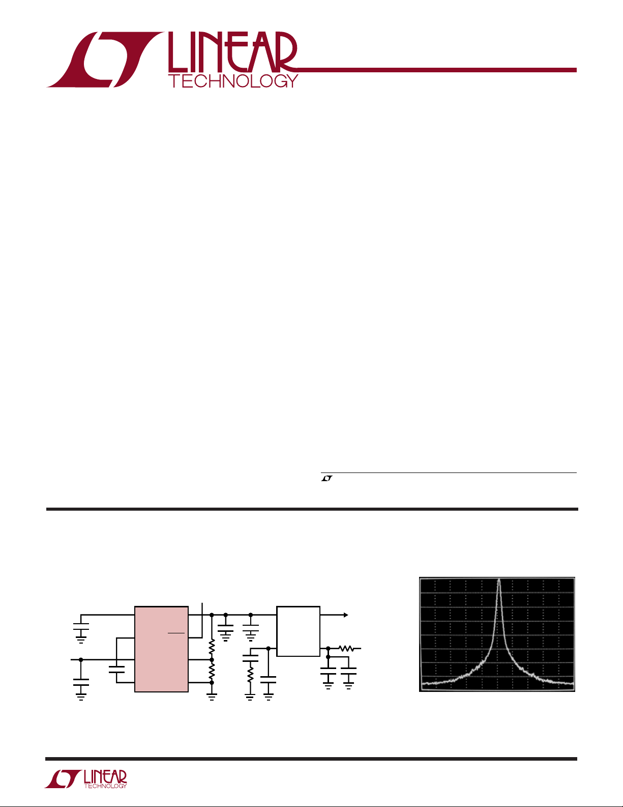
TYPICAL APPLICATIO
4.2V VCO Power Supply, VIN = 2.5V to 4.4V
SHUTDOWN
V
2.5V TO
4.4V
8
CPO
4.7µF
IN
0.22µF
4.7µF
7
C
6
V
5
C
+
LTC1682
IN
–
V
OUT
SHDN
GND
FB
U
Open-Loop Close-In Phase Noise
4.2V
1
2
3
4
36k
15k
4.7µF
1µF
1k
1000pF
B
VCO
MURATA
MQE001-902
M
1000pF
1000pF
P
C
100k
f
OUT
902MHz
V
4.7µF
1682 TA01
C
AMPLITUDE
10dB/DIV
CENTER = 902MHz RES BW = 1kHz
SPAN = 100kHz VBW = 30Hz
SWP = 10 sec REF = 0dBm
1682 TA02
1
LTC1682/LTC1682-3.3/LTC1682-5
TOP VIEW
S8 PACKAGE
8-LEAD PLASTIC SO
1
2
3
4
8
7
6
5
V
OUT
SHDN
FILT/FB*
GND
CPO
C
+
V
IN
C
–
*PIN3 = FILT FOR LTC1682-3.3/LTC1682-5
= FB FOR LTC1682
WW
W
ABSOLUTE MAXIMUM RATINGS
U
(Note 1)
VIN to Ground ..............................................–0.3V to 5V
V
Voltage................................................–0.3V to 6V
OUT
CPO to Ground ........................................................ 10V
SHDN, FILT/FB Voltage to
Ground ..................................... – 0.3V to (VIN + 0.3V)
V
Short-Circuit Duration............................ Indefinite
OUT
I
...................................................................... 90mA
OUT
UUW
PACKAGE/ORDER INFORMATION
ORDER PART
NUMBER
TOP VIEW
V
1
OUT
2
SHDN
3
FILT/FB*
4
GND
MS8 PACKAGE
8-LEAD PLASTIC MSOP
*PIN3 = FILT FOR LTC1682-3.3/LTC1682-5
= FB FOR LTC1682
T
= 125°C, θJA = 140°C/ W
JMAX
8
CPO
+
7
C
V
6
IN
–
C
5
LTC1682CMS8
LTC1682CMS8-3.3
LTC1682CMS8-5
LTC1682IMS8
LTC1682IMS8-3.3
LTC1682IMS8-5
MS8 PART MARKING
LTER
LTGT
LTGV
LTHM
LTGU
LTGW
Operating Temperature Range
Commercial ............................................ 0°C to 70°C
Extended Commercial (Note 2)........... – 40°C to 85°C
Industrial ........................................... –40°C to 85°C
Storage Temperature Range ................. –65°C to 150°C
Lead Temperature (Soldering, 10 sec)..................300°C
Maximum Junction Temperature..........................125°C
ORDER PART
NUMBER
LTC1682CS8
LTC1682CS8-3.3
LTC1682CS8-5
LTC1682IS8
LTC1682IS8-3.3
LTC1682IS8-5
S8 PART MARKING
= 125°C, θJA = 120°C/W
T
JMAX
1682
168233
16825
1682I
1682I33
1682I5
Consult factory for Military grade parts.
ELECTRICAL CHARACTERISTICS
range, otherwise specifications are TA = 25°C. SHDN = VIN = 3V; C1 = 0.22µF; C2, C3, C4 = 4.7µF, unless otherwise noted.
PARAMETER CONDITIONS MIN TYP MAX UNITS
VIN Operating Voltage LTC1682 ● 1.8 4.4 V
I
Shutdown Current SHDN = 0V ● 15 µA
VIN
I
Operating Current I
VIN
FB Input Current LTC1682, FB = 1.235V ● –50 50 nA
FB Voltage LTC1682 ● 1.210 1.235 1.260 V
Regulated Output Voltage LTC1682-3.3, I
V
Temperature Coefficient ±50 ppm
OUT
Charge Pump Oscillator Frequency I
Burst Mode is a trademark of Linear Technology Corporation.
2
The ● denotes specifications that apply over the full operating temperature
LTC1682-3.3
LTC1682-5
= 0mA, Burst Mode
OUT
0°C to 70°C
–40°C to 85°C
LTC1682-5, I
> 200µA, VIN = 1.8V to 4.4V ● 480 550 620 kHz
OUT
OUT
OUT
TM
Operation
= 1mA ● 3.23 3.30 3.37 V
= 1mA ● 4.9 5.0 5.1 V
● 2 4.4 V
● 2.7 4.4 V
● 150 250 µA
● 150 300 µA
LTC1682/LTC1682-3.3/LTC1682-5
ELECTRICAL CHARACTERISTICS
The ● denotes specifications that apply over the full operating temperature
range, otherwise specifications are TA = 25°C. SHDN = VIN = 3V; C1 = 0.22µF; C2, C3, C4 = 4.7µF, unless otherwise noted.
PARAMETER CONDITIONS MIN TYP MAX UNITS
CPO (Charge Pump Output) VIN = 1.8V, I
Output Resistance V
V
Dropout Voltage (Note 3) LTC1682, I
OUT
= 3V, I
IN
= 4.4V, I
V
IN
LTC1682/LTC1682-3.3, I
LTC1682/LTC1682-5, I
V
Enable Time I
OUT
V
Output Noise Voltage LTC1682 I
OUT
= 10mA 2 ms
OUT
LTC1682-3.3 I
LTC1682-5 I
V
Line Regulation VIN = 3V to 4V, I
OUT
V
Load Regulation I
OUT
V
Shutdown Resistance SHDN = 0V, Resistance Measured to Ground, VIN = 1.8V ● 150 350 Ω
OUT
= 1mA to 10mA ● 310 mV
OUT
I
= 1mA to 50mA (Note 4) 10 mV
OUT
SHDN = 0V, Resistance Measured to Ground, V
SHDN Input Threshold VIN = 1.8V to 4.4V ● 0.4 1 1.6 V
SHDN Input Current SHDN = V
SHDN = 0V
= 10mA ● 18 30 Ω
OUT
= 10mA ● 13 20 Ω
OUT
= 10mA ● 11 17 Ω
OUT
= 10mA, V
OUT
IN
OUT
I
OUT
OUT
I
OUT
OUT
I
OUT
= 0mA (Note 6) ● 520 mV
OUT
= 2.57V (Note 5) ● 100 160 mV
OUT
= 10mA, V
OUT
= 10mA, V
OUT
= 10mA, 10Hz ≤ f ≤ 100kHz, V
= 10mA, 10Hz ≤ f ≤ 2.5MHz, V
= 10mA, 10Hz ≤ f ≤ 100kHz, C
= 10mA, 10Hz ≤ f ≤ 2.5MHz, C
= 10mA, 10Hz ≤ f ≤ 100kHz, C
= 10mA, 10Hz ≤ f ≤ 2.5MHz, C
= 3.3V ● 75 120 mV
OUT
= 5V ● 50 90 mV
OUT
= 5V 88 µV
OUT
= 5V 800 µV
OUT
= 1nF 58 µV
FILT
= 1nF 500 µV
FILT
= 1nF 64 µV
FILT
= 1nF 600 µV
FILT
= 4.4V ● 50 150 Ω
IN
● –1 1 µA
● –1 1 µA
RMS
P-P
RMS
P-P
RMS
P-P
Note 1: Absolute Maximum Ratings are those values beyond which the life
of a device may be impaired.
Note 2: The LTC1682C is guaranteed to meet specified performance from
0°C to 70°C and is designed, characterized and expected to meet these
extended temperature limits, but is not tested at –40°C and 85°C. The
LTC1682I is guaranteed to meet the extended temperature limits.
Note 3: Dropout voltage is the minimum input/output voltage required to
maintain regulation at the specified output current. In dropout the output
voltage will be equal to: V
CPO
– V
DROPOUT
(see Figure 4).
Note 4: Operating conditions are limited by maximum junction
temperature. The regulated output specification will not apply for all
possible combinations of input voltage and output current. When
operating at maximum input voltage, the output current range may be
limited. When operating at maximum output current, the input voltage
range may be limited.
Note 5: Limited by the LDO disable switch point of 1.45V
.
IN
Note 6: The LTC1682 is set to 5V. The feedback current is 25µA.
3
LTC1682/LTC1682-3.3/LTC1682-5
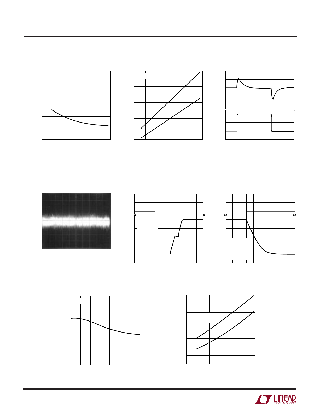
UW
TYPICAL PERFOR A CE CHARACTERISTICS
CPO Output Resistance vs V
35
30
25
(Ω)
20
CPO
R
15
10
5
1.5
2.5 3.0 3.5
2.0
VIN (V)
LTC1682-5 Output Noise
(BW = 10Hz to 2.5MHz)
IN
TA = 25°C
C1 = 0.22µF
= 10mA
I
OUT
4.0 4.5
1682 G01
Min and Max V
9
TA = 25°C
8
7
6
(V)
CPO
V
5
4
3
1.5
(A) THE MAXIMUM GENERATED NO LOAD
(B) THE MINIMUM ALLOWABLE CPO VOLTAGE,
V
2.5 3.0 3.5
2.0
CPO VOLTAGE
AT FULL LOAD, TO ENSURE THAT THE LDO
IS NOT DISABLED
Shutdown to Enable Timing
CPO
vs V
CPO
= 2(VIN)
(A)
V
VIN (V)
IN
(B)
= 1.45(VIN)
CPO
4.0 4.5
1682 G02
V
Transient Response
OUT
10
5
(mV)I
0
OUT
TA = 25°C
∆V
(mA)
OUT
V
–5
IN
V
OUT
C
–10
OUT
15
10
5
0
050
= 3V
= 4V
= 10µF
100 200150
TIME (µs)
Enable to Shutdown Timing
250
300
1682 G02
V
OUT
200µV/DIV
C
= C
CPO
= 10mA TA = 25°C
I
OUT
= 3V C
V
IN
100µs/DIV 1682 G04
= 4.7µFV
OUT
Oscillator Frequency vs
Temperature
565
VIN = 3V
560
555
550
545
540
OSCILLATION FREQUENCY (kHz)
535
530
–50
= 5V
OUT
= 1nF
FILT
–25 0
50 100 125
25 75
TEMPERATURE (°C)
SHDN (V)V
(V)
OUT
2
0
4
3
2
1
0
1682 G07
TA = 25°C
= 3V
V
IN
= 4V
V
OUT
= 10mA
I
OUT
= C
C
CPO
OUT
= 10µF
200µs/DIV
1682 G05
Operating Current vs V
(No Load)
220
TA = 25°C
200
180
160
140
120
100
OPERATING CURRENT (µA)
80
60
1.5
LTC1682-3.3
LTC1682-5
2.5 3.0 3.5 4.0 4.5
2.0
2
0
SHDN (V)V
4
3
(V)
2
OUT
1
0
VIN (V)
NO LOAD
= 25°C
T
A
= 3V
V
IN
= 4V
V
OUT
= 10µF
C
OUT
IN
LTC1682
1ms/DIV
1682 G06
1682 G08
4
 Loading...