

FEATURES
LTC1666/LTC1667/LTC1668
12-Bit, 14-Bit, 16-Bit,
U
50Msps DACs
DESCRIPTIO
■
50Msps Update Rate
■
Pin Compatible 12-Bit, 14-Bit and 16-Bit Devices
■
High Spectral Purity: 87dB SFDR at 1MHz f
■
5pV-s Glitch Impulse
■
Differential Current Outputs
■
20ns Settling Time
■
Low Power: 180mW from ±5V Supplies
■
TTL/CMOS (3.3V or 5V) Inputs
■
Small Package: 28-Pin SSOP
OUT
U
APPLICATIO S
■
Cellular Base Stations
■
Multicarrier Base Stations
■
Wireless Communication
■
Direct Digital Synthesis (DDS)
■
xDSL Modems
■
Arbitrary Waveform Generation
■
Automated Test Equipment
■
Instrumentation
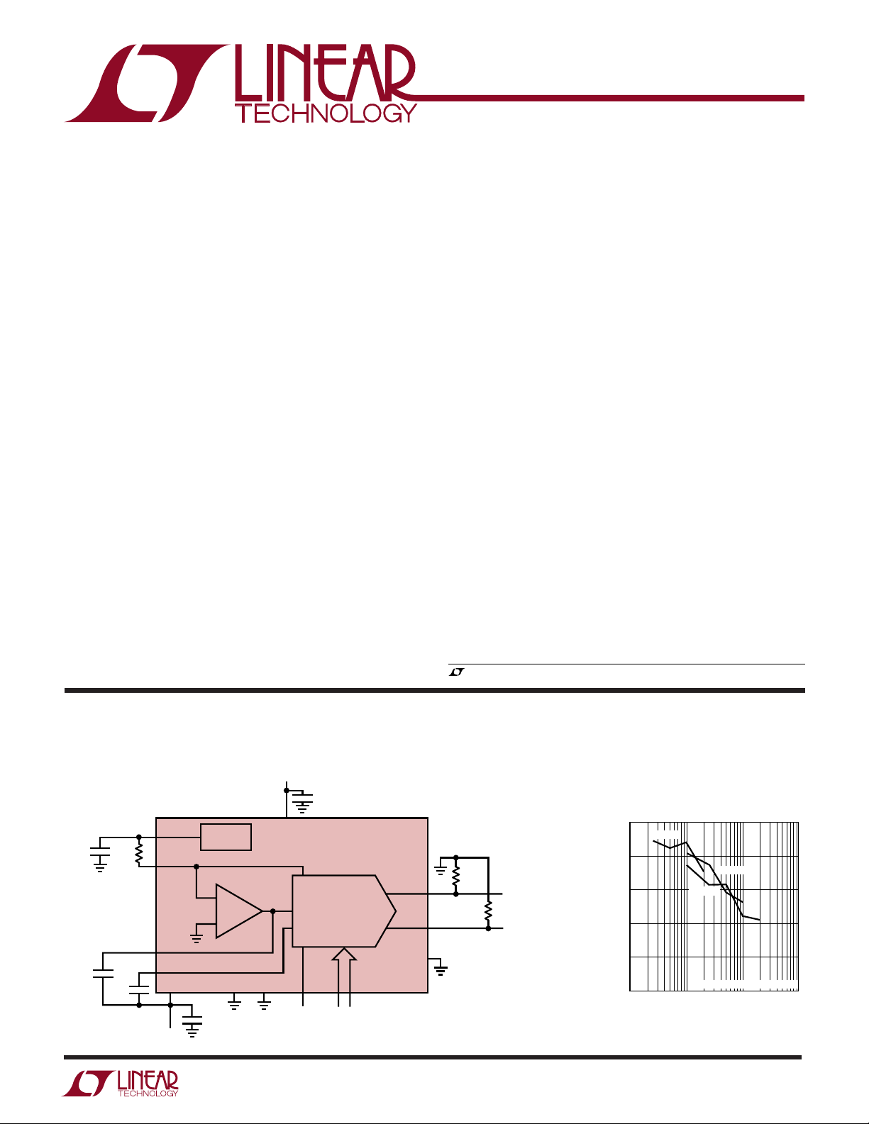
The LTC®1666/LTC1667/LTC1668 are 12-/14-/16-bit,
50Msps differential current output DACs implemented on
a high performance BiCMOS process with laser trimmed,
thin-film resistors. The combination of a novel currentsteering architecture and a high performance process
produces DACs with exceptional AC and DC performance.
The LTC1668 is the first 16-bit DAC in the marketplace to
exhibit an SFDR (spurious free dynamic range) of 87dB
for an output signal frequency of 1MHz.
Operating from ±5V supplies, the
LTC1668
can be configured to provide full-scale output
LTC1666/LTC1667/
currents up to 10mA. The differential current outputs of
the DACs allow single-ended or true differential operation.
The –1V to 1V output compliance of the
LTC1667/LTC1668
allows the outputs to be connected
LTC1666/
directly to external resistors to produce a differential output voltage without degrading the converter’s linearity. Alternatively, the outputs can be connected to the summing
junction of a high speed operational amplifier, or to a
transformer.
TYPICAL APPLICATION
LTC1668, 16-Bit, 50Msps DAC
5V
V
0.1µF
0.1µF
REFOUT
R
SET
2k
I
REFIN
COMP1
C1
C2
0.1µF
COMP2
V
SS
–5V
2.5V
REFERENCE
+
–
AGND DGND CLK DB15 DB0
0.1µF
U
DD
CLOCK
INPUT
0.1µF
16-BIT
HIGH SPEED
DAC
16-BIT DATA
INPUT
LTC1668
I
OUT A
I
OUT B
LADCOM
1666/7/8 TA01
The LTC1666/LTC1667/LTC1668 are pin compatible and
are available in a 28-pin SSOP and are fully specified over
the industrial temperature range.
, LTC and LT are registered trademarks of Linear Technology Corporation.
52.3Ω
52.3Ω V
+
1V
OUT
DIFFERENTIAL
–
LTC1668 SFDR vs f
100
5MSPS
90
80
P-P
SFDR (dB)
70
60
50
0.1
50MSPS
DIGITAL AMPLITUDE = 0dBFS
1.0 10 100
f
OUT
25MSPS
(MHz)
OUT
and f
CLOCK
1666/7/8 G05
1
LTC1666/LTC1667/LTC1668
WWWU
ABSOLUTE AXI U RATI GS
(Note 1)
Supply Voltage (VDD)................................................ 6V
Negative Supply Voltage (VSS) ............................... – 6V
Total Supply Voltage (VDD to VSS) .......................... 12V
Digital Input Voltage ....................–0.3V to (VDD + 0.3V)
Analog Output Voltage
(I
OUT A
and I
) ........ (VSS – 0.3V) to (VDD + 0.3V)
OUT B
UU
W
PACKAGE/ORDER I FOR ATIO
1
DB9
2
DB8
3
DB7
4
DB6
5
DB5
6
DB4
7
DB3
8
DB2
9
DB1
NC
NC
NC
NC
10
11
12
13
14
DB0 (LSB)
Power Dissipation............................................. 500mW
Operating Temperature Range
LTC1666C/LTC1667C/LTC1668C ........... 0°C to 70°C
LTC1666I/LTC1667I/LTC1668I.......... – 40°C to 85°C
Storage Temperature Range ................ –65°C to 150°C
Lead Temperature (Soldering, 10 sec).................. 300°C
TOP VIEW
DB10
28
DB11 (MSB)
27
CLK
26
V
25
DGND
24
V
23
COMP2
22
COMP1
21
I
20
I
19
LADCOM
18
AGND
17
I
16
REFOUT
15
DD
SS
OUT A
OUT B
REFIN
ORDER PART
NUMBER
LTC1666CG
LTC1666IG
G PACKAGE
28-LEAD PLASTIC SSOP
T
= 110°C, θJA = 100°C/W
JMAX
DB11
DB10
DB9
DB8
DB7
DB6
DB5
DB4
DB3
DB2
DB1
DB0 (LSB)
NC
NC
TOP VIEW
1
2
3
4
5
6
7
8
9
10
11
12
13
14
G PACKAGE
28-LEAD PLASTIC SSOP
T
= 110°C, θJA = 100°C/W T
JMAX
DB12
28
DB13 (MSB)
27
CLK
26
V
25
DGND
24
V
23
COMP2
22
COMP1
21
I
20
I
19
LADCOM
18
AGND
17
I
16
REFOUT
15
DD
SS
OUT A
OUT B
REFIN
ORDER PART
NUMBER
LTC1667CG
LTC1667IG
Consult LTC Marketing for parts specified with wider operating temperature ranges.
DB13
DB12
DB11
DB10
DB9
DB8
DB7
DB6
DB5
DB4
DB3
DB2
DB1
DB0 (LSB)
TOP VIEW
1
2
3
4
5
6
7
8
9
10
11
12
13
14
G PACKAGE
28-LEAD PLASTIC SSOP
= 110°C, θJA = 100°C/W
JMAX
DB14
28
DB15 (MSB)
27
CLK
26
V
25
DGND
24
V
23
COMP2
22
COMP1
21
I
20
I
19
LADCOM
18
AGND
17
I
16
REFOUT
15
DD
SS
OUT A
OUT B
REFIN
ORDER PART
NUMBER
LTC1668CG
LTC1668IG
2
LTC1666/LTC1667/LTC1668
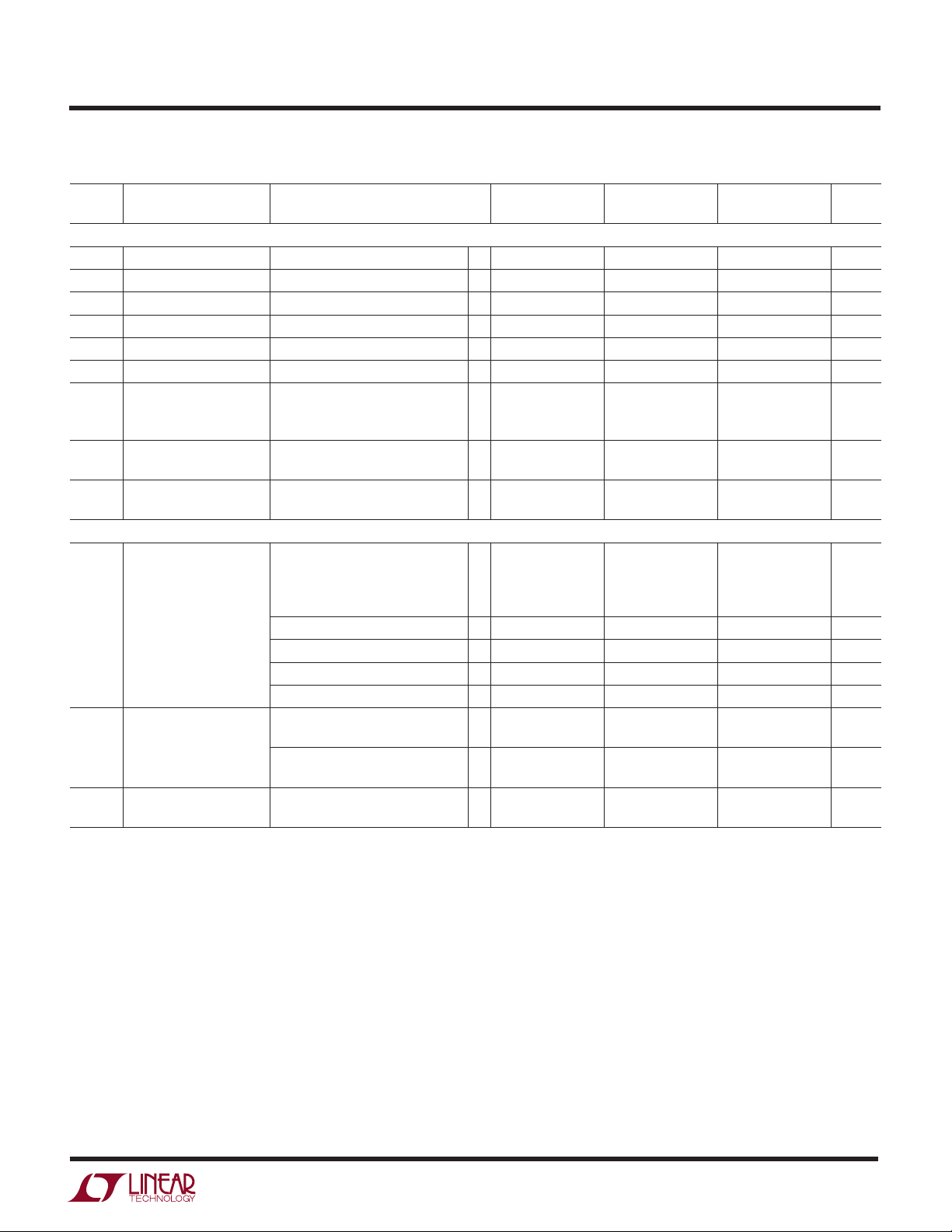
ELECTRICAL CHARACTERISTICS
temperature range, otherwise specifications are at TA = 25°C. VDD = 5V, VSS = –5V, LADCOM = AGND = DGND = 0V, I
The ● denotes specifications which apply over the full operating
= 10mA.
OUTFS
LTC1666 LTC1667 LTC1668
SYMBOL PARAMETER CONDITIONS MIN TYP MAX MIN TYP MAX MIN TYP MAX UNITS
DC Accuracy (Measured at I
, Driving a Virtual Ground)
OUT A
Resolution ● 12 14 16 Bits
Monotonicity 12 14 14 Bits
INL Integral Nonlinearity (Note 2) ±1 ±2 ±8 LSB
DNL Differential Nonlinearity (Note 2) ±1 ±1 ±1 ±4 LSB
Offset Error 0.1 ±0.2 0.1 ±0.2 0.1 ±0.2 % FSR
Offset Error Drift 5 5 5 ppm/°C
GE Gain Error Internal Reference, R
= 2k 2 2 2 % FSR
IREFIN
External Reference, 1 1 1 % FSR
V
REF
= 2.5V, R
IREFIN
= 2k
Gain Error Drift Internal Reference 50 50 50 ppm/°C
External Reference 30 30 30 ppm/°C
PSRR Power Supply VDD = 5V ±5% ±0.1 ±0.1 ±0.1 % FSR/V
Rejection Ratio V
= –5V ±5% ±0.2 ±0.2 ±0.2 % FSR/V
SS
AC Linearity
SFDR Spurious Free Dynamic f
= 25Msps, f
CLK
OUT
= 1MHz
Range to Nyquist 0dB FS Output 76 78 78 87 dB
–6dB FS Output 87 dB
–12dB FS Output 83 dB
f
Spurious Free Dynamic f
Range Within a Window f
THD Total Harmonic Distortion f
= 50Msps, f
CLK
f
= 50Msps, f
CLK
f
= 50Msps, f
CLK
f
= 50Msps, f
CLK
= 25Msps, 85 86 86 96 dB
CLK
= 1MHz, 2MHz Span
OUT
f
= 50Msps, 88 dB
CLK
= 5MHz, 4MHz Span
f
OUT
= 25Msps, f
CLK
= 50Msps, f
f
CLK
= 1MHz 85 dB
OUT
= 2.5MHz 81 dB
OUT
= 5MHz 79 dB
OUT
= 20MHz 70 dB
OUT
= 1MHz –75 –77 –84 – 77 dB
OUT
= 5MHz –78 dB
OUT
3
LTC1666/LTC1667/LTC1668
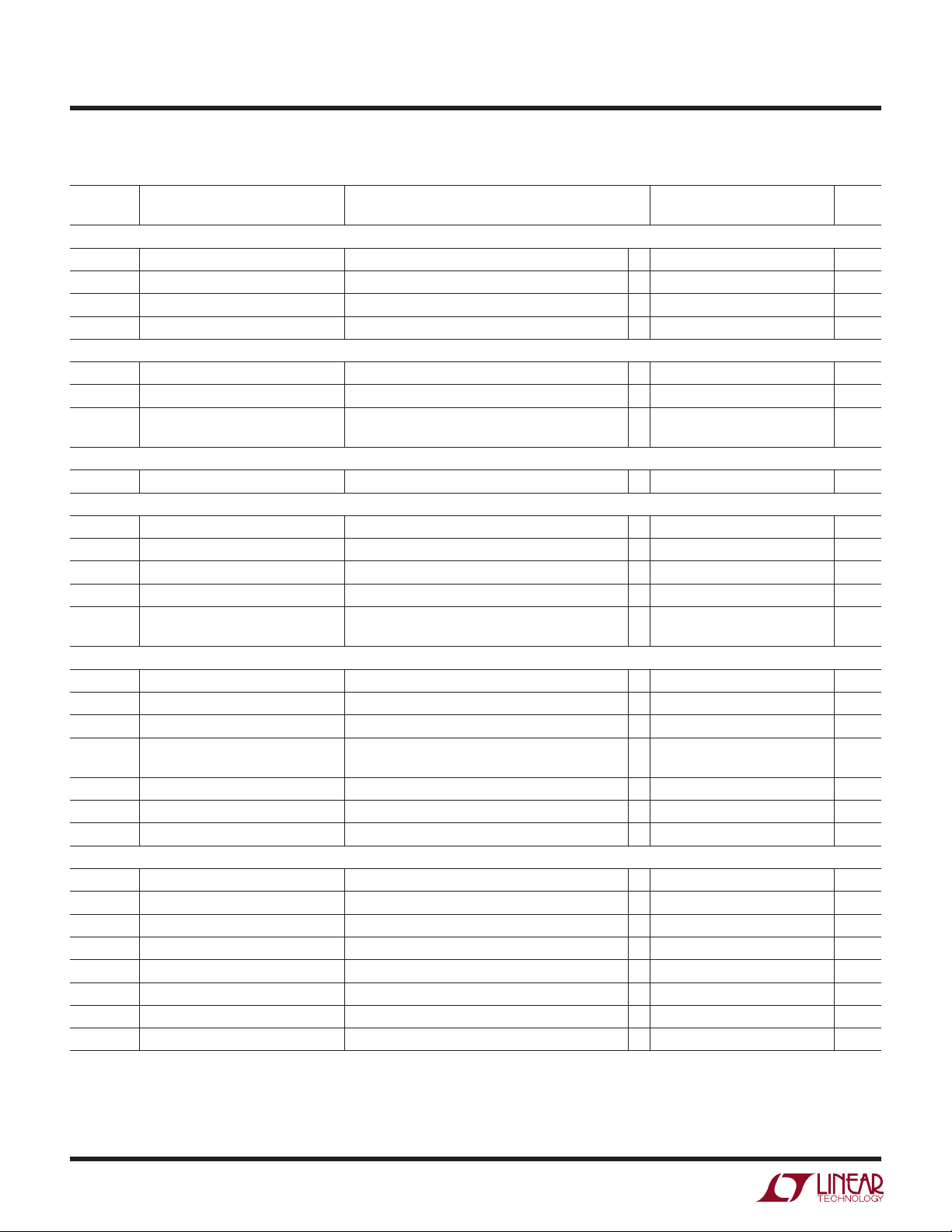
ELECTRICAL CHARACTERISTICS
temperature range, otherwise specifications are at TA = 25°C. VDD = 5V, VSS = –5V, LADCOM = AGND = DGND = 0V, I
The ● denotes specifications which apply over the full operating
= 10mA.
OUTFS
LTC1666/LTC1667/LTC1668
SYMBOL PARAMETER CONDITIONS MIN TYP MAX UNITS
Analog Output
I
OUTFS
Full-Scale Output Current ● 110mA
Output Compliance Range IFS = 10mA ● –1 1 V
Output Resistance; R
IOUT A
, R
IOUT BIOUT A, B
to LADCOM ● 0.7 1.1 1.5 kΩ
Output Capacitance 5pF
Reference Output
Reference Voltage REFOUT Tied to I
Through 2kΩ 2.475 2.5 2.525 V
REFIN
Reference Output Drift 25 ppm/°C
Reference Output Load Regulation I
= 0mA to 5mA 6 mV/mA
LOAD
Reference Input
Reference Small-Signal Bandwidth IFS = 10mA, C
= 0.1µF 20 kHz
COMP1
Power Supply
V
DD
V
SS
I
DD
I
SS
P
DIS
Positive Supply Voltage ● 4.75 5 5.25 V
Negative Supply Voltage ● –4.75 –5 –5.25 V
Positive Supply Current IFS = 10mA, f
Negative Supply Current IFS = 10mA, f
Power Dissipation IFS = 10mA, f
= 1mA, f
I
FS
= 25Msps, f
CLK
= 25Msps, f
CLK
= 25Msps, f
CLK
= 25Msps, f
CLK
= 1MHz ● 35mA
OUT
= 1MHz ● 33 40 mA
OUT
= 1MHz 180 mW
OUT
= 1MHz 85 mW
OUT
Dynamic Performance (Differential Transformer Coupled Output, 50Ω Double Terminated, Unless Otherwise Noted)
f
CLOCK
t
S
t
PD
Maximum Update Rate ● 50 75 Msps
Output Settling Time To 0.1% FSR 20 ns
Output Propagation Delay 8ns
Glitch Impulse Single Ended 15 pV-s
Differential 5 pV-s
t
r
t
f
i
NO
Output Rise Time 4ns
Output Fall Time 4ns
Output Noise 50 pA/√Hz
Digital Inputs
V
IH
V
IL
I
IN
C
IN
t
DS
t
DH
t
CLKH
t
CLKL
Note 1: Absolute Maximum Ratings are those values beyond which the life
of the device may be impaired.
Digital High Input Voltage ● 2.4 V
Digital Low Input Voltage ● 0.8 V
Digital Input Current ● ±10 µA
Digital Input Capacitance 5pF
Input Setup Time ● 8ns
Input Hold Time ● 4ns
Clock High Time ● 5ns
Clock Low Time ● 8ns
Note 2: For the LTC1666, ±1LSB = ±0.024% of full scale;
for the LTC1667, ±1LSB = ±0.006% of full scale = ±61ppm of full scale;
for the LTC1668, ±1LSB = ±0.0015% of full scale = ±15.3ppm of full scale.
4
LTC1666/LTC1667/LTC1668
f
OUT
(MHz)
0
SFDR (dB)
10
95
90
85
80
75
70
65
60
55
50
1666/7/8 G09
2.5 5 7.5
DIGITAL AMPLITUDE = 0dBFS
I
OUTFS
= 2.5mA
I
OUTFS
= 5mA
I
OUTFS
= 10mA
UW
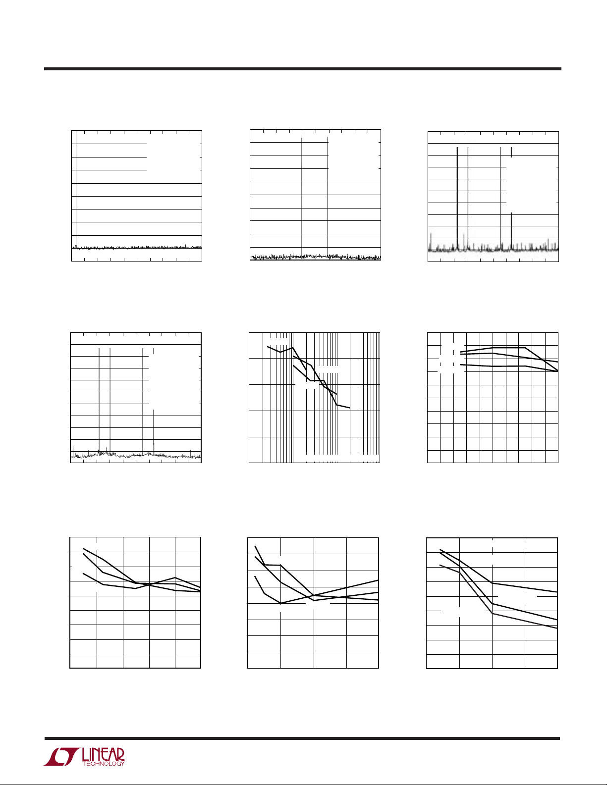
TYPICAL PERFOR A CE CHARACTERISTICS
(LTC1668)
Single Tone SFDR at 50MSPS 2-Tone SFDR
0
–10
–20
–30
–40
–50
–60
–70
SIGNAL AMPLITUDE (dBFS)
–80
–90
–100
05
FREQUENCY (MHz)
4-Tone SFDR, f
0
–10
–20
–30
–40
–50
–60
–70
–80
SIGNAL AMPLITUDE (dBFS)
–90
–100
–110
0.1 0.46 0.82 1.18 1.54 1.9
FREQUENCY (MHz)
10
CLOCK
SFDR = 87dB
f
CLOCK
= 1.002MHz
f
OUT
AMPL = 0dBFS
15 20 25
= 5MSPS
SFDR > 82dB
f
CLOCK
f
OUT1
f
OUT2
f
OUT3
f
OUT4
AMPL = 0dBFS
= 50MSPS
= –8.25dBm
1666/7/8 G01
= 5MSPS
= 0.5MHz
= 0.65MHz
= 1.10MHz
= 1.25MHz
1666/7/8 G04
0
–10
–20
–30
–40
–50
–60
–70
SIGNAL AMPLITUDE (dBFS)
–80
–90
–100
4.5 5.0 5.5
SFDR vs f
100
90
80
SFDR (dB)
70
60
50
0.1
SFDR > 86dB
f
CLOCK
f
OUT1
f
OUT2
AMPL = 0dBFS
FREQUENCY (MHz)
and f
OUT
5MSPS
1.0 10 100
CLOCK
25MSPS
50MSPS
DIGITAL AMPLITUDE = 0dBFS
f
(MHz)
OUT
= 50MSPS
= 4.9MHz
= 5.09MHz
1666/7/8 G02
1666/7/8 G05
4-Tone SFDR, f
0
–10
–20
–30
–40
–50
–60
–70
–80
SIGNAL AMPLITUDE (dBFS)
–90
–100
–110
1 4.6 8.2 11.8 15.4 19
FREQUENCY (MHz)
SFDR vs f
(dBFS) at f
100
95
90
85
80
75
SFDR (dB)
70
65
60
55
50
0 0.4
0dBFS
–6dBFS
–12dBFS
and Digital Amplitude
OUT
CLOCK
0.8
CLOCK
= 5MSPS
1.2 1.6 2.0
f
(MHz)
OUT
= 50MSPS
SFDR > 74dB
f
CLOCK
f
OUT1
f
OUT2
f
OUT3
f
OUT4
AMPL = 0dBFS
= 50MSPS
= 5.02MHz
= 6.51MHz
= 11.02MHz
= 12.51MHz
1666/7/8 G03
1666/7/8 G06
SFDR vs f
(dBFS) at f
95
90
85
80
75
70
SFDR (dB)
65
60
55
50
0dBFS
–6dBFS
–12dBFS
0
and Digital Amplitude
OUT
= 25MSPS
CLOCK
26
4
f
(MHz)
OUT
8
1666/7/8 G07
SFDR vs f
(dBFS) at f
90
85
80
75
70
SFDR (dB)
65
60
55
10
50
–12dBFS
0
and Digital Amplitude
OUT
= 50MSPS
CLOCK
0dBFS
–6dBFS
515
f
OUT
10
(MHz)
20
1666/7/8 G08
SFDR vs f
f
= 25MSPS
CLOCK
OUT
and I
OUTFS
at
5
LTC1666/LTC1667/LTC1668
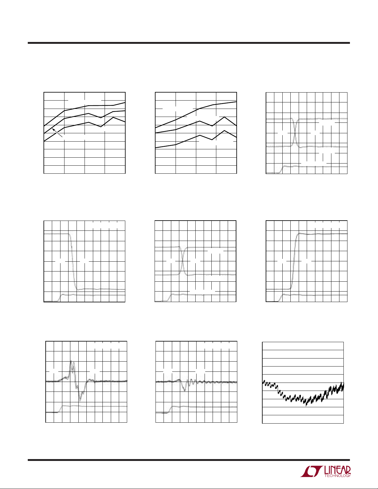
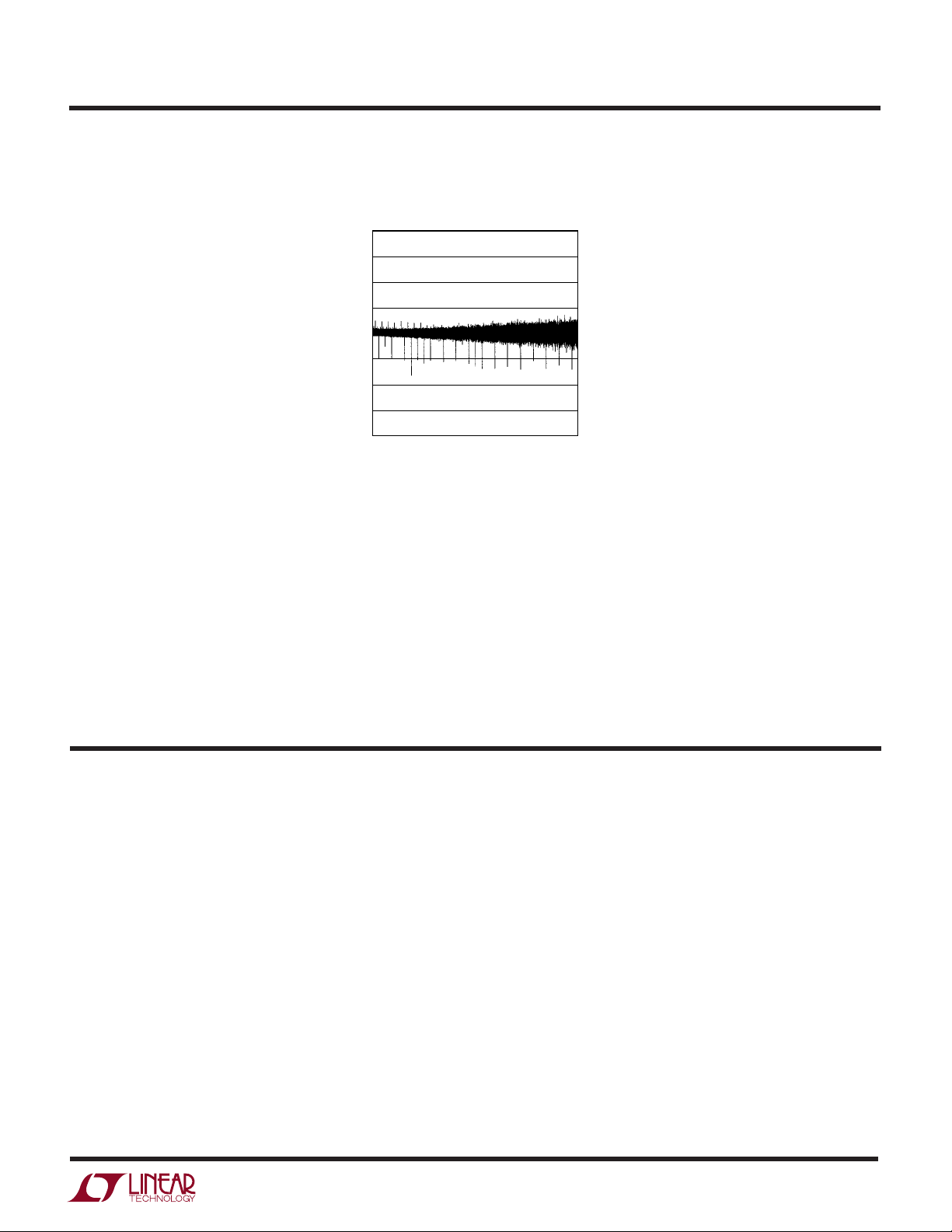
100mV
/DIV
CLK IN
5V/DIV
1666/7/8 G12
5ns/DIV
V(I
OUTB
)
V(I
OUTA
)
FFFF
0000
CLOCK INPUT
UW
TYPICAL PERFOR A CE CHARACTERISTICS
(LTC1668)
SFDR vs Digital Amplitude (dBFS)
and f
100
95
90
85
80
75
SFDR (dB)
70
65
60
55
50
–20 –15 –10 –5 0
at f
CLOCK
2.277MHz AT 25MSPS
DIGITAL AMPLITUDE (dBFS)
= f
OUT
CLOCK
455kHz AT 5MSPS
4.55MHz AT 50MSPS
Differential Output
Full-Scale Transition
V(I
OUTA
100mV
/DIV
0000
FFFF
/11
) – V(I
1666/7/8 G10
OUTB
SFDR vs Digital Amplitude (dBFS)
and f
100
95
90
85
80
75
SFDR (dB)
70
65
60
55
50
–20 –15 –10 –5 0
at f
CLOCK
1MHz AT 5MSPS
DIGITAL AMPLITUDE (dBFS)
= f
OUT
5MHz AT 25MSPS
/5
CLOCK
10MHz AT 50MSPS
1666/7/8 G11
Single-Ended Output
Full-Scale Transition
)
V(I
)
OUTA
100mV
/DIV
FFFF
0000
Single-Ended Outputs
Full-Scale Transition
Differential Output
Full-Scale Transition
100mV
/DIV
FFFF
0000
V(I
OUTA
) – V(I
OUTB
)
CLK IN
5V/DIV
Single-Ended Midscale
Glitch Impulse
7FFF
1mV/DIV
CLK IN
5V/DIV
5ns/DIV
5ns/DIV
V(I
8000
OUTA
), V(I
1666/7/8 G13
OUTB
1666/7/8 G16
V(I
)
OUTB
CLK IN
5V/DIV
CLOCK INPUT
5ns/DIV
1666/7/8 G14
CLK IN
5V/DIV
5ns/DIV
1666/7/8 G15
Differential Midscale
Glitch Impulse
)
7FFF
1mV/DIV
CLK IN
5V/DIV
8000
5ns/DIV
V(I
OUTA
) – V(I
)
OUTB
1666/7/8 G17
Integral Nonlinearity
5
4
3
2
1
0
–1
–2
–3
INTEGRAL NONLINEARITY (LSB)
–4
–5
16384
32768
DIGITAL INPUT CODE
49152
65535
1666/7/8 G18
6
LTC1666/LTC1667/LTC1668
UW
TYPICAL PERFOR A CE CHARACTERISTICS
Differential Nonlinearity
2.0
1.5
1.0
0.5
0
–0.5
–1.0
DIFFERENTIAL NONLINEARITY (LSB)
–1.5
–2.0
0
16384
32768
DIGITAL INPUT CODE
49152
1666/7/8 G19
(LTC1668)
65535
U
UU
PI FU CTIO S
LTC1666
REFOUT (Pin 15): Internal Reference Voltage Output.
Nominal value is 2.5V. Requires a 0.1µF bypass capacitor
to AGND.
I
(Pin 16): Reference Input Current. Nominal value is
REFIN
1.25mA for IFS = 10mA. IFS = I
AGND (Pin 17): Analog Ground.
LADCOM (Pin 18): Attenuator Ladder Common. Normally
tied to GND.
I
(Pin 19): Complementary DAC Output Current. Full-
OUT B
scale output current occurs when all data bits are 0s.
I
(Pin 20): DAC Output Current. Full-scale output
OUT A
current occurs when all data bits are 1s.
REFIN
• 8.
COMP1 (Pin 21): Current Source Control Amplifier Compensation. Bypass to VSS with 0.1µF.
COMP2 (Pin 22): Internal Bypass Point. Bypass to V
SS
with 0.1µF.
VSS (Pin 23): Negative Supply Voltage. Nominal value is
–5V.
DGND (Pin 24): Digital Ground.
VDD (Pin 25): Positive Supply Voltage. Nominal value is 5V.
CLK (Pin 26): Clock Input. Data is latched and the output
is updated on positive edge of clock.
DB11 to DB0 (Pins 27, 28, 1 to 10 ): Digital Input Data Bits.
7

LTC1666/LTC1667/LTC1668
U
UU
PI FU CTIO S
LTC1667
REFOUT (Pin 15): Internal Reference Voltage Output.
Nominal value is 2.5V. Requires a 0.1µF bypass capacitor
to AGND.
I
(Pin 16): Reference Input Current. Nominal value is
REFIN
1.25mA for IFS = 10mA. IFS = I
AGND (Pin 17): Analog Ground.
LADCOM (Pin 18): Attenuator Ladder Common. Normally
tied to GND.
I
(Pin 19): Complementary DAC Output Current. Full-
OUT B
scale output current occurs when all data bits are 0s.
I
(Pin 20): DAC Output Current. Full-scale output
OUT A
current occurs when all data bits are 1s.
COMP1 (Pin 21): Current Source Control Amplifier Com-
pensation. Bypass to VSS with 0.1µF.
REFIN
• 8.
LTC1668
REFOUT (Pin 15): Internal Reference Voltage Output.
Nominal value is 2.5V. Requires a 0.1µF bypass capacitor
to AGND.
I
(Pin 16): Reference Input Current. Nominal value is
REFIN
1.25mA for IFS = 10mA. IFS = I
AGND (Pin 17): Analog Ground.
LADCOM (Pin 18): Attenuator Ladder Common. Normally
tied to GND.
I
(Pin 19): Complementary DAC Output Current. Full-
OUT B
scale output current occurs when all data bits are 0s.
I
(Pin 20): DAC Output Current. Full-scale output
OUT A
current occurs when all data bits are 1s.
COMP1 (Pin 21): Current Source Control Amplifier Com-
pensation. Bypass to VSS with 0.1µF.
REFIN
• 8.
COMP2 (Pin 22): Internal Bypass Point. Bypass to V
with 0.1µF.
VSS (Pin 23): Negative Supply Voltage. Nominal value is
–5V.
DGND (Pin 24): Digital Ground.
VDD (Pin 25): Positive Supply Voltage. Nominal value is 5V.
CLK (Pin 26): Clock Input. Data is latched and the output
is updated on positive edge of clock.
DB13 to DB0 (Pins 27, 28, 1 to 12 ): Digital Input Data Bits.
SS
COMP2 (Pin 22): Internal Bypass Point. Bypass to V
with 0.1µF.
VSS (Pin 23): Negative Supply Voltage. Nominal value is
–5V.
DGND (Pin 24): Digital Ground.
VDD (Pin 25): Positive Supply Voltage. Nominal value is 5V.
CLK (Pin 26): Clock Input. Data is latched and the output
is updated on positive edge of clock.
DB15 to DB0 (Pins 27, 28, 1 to 14 ): Digital Input Data Bits.
SS
8
 Loading...