

Linear Technology LTC1665, LTC1660 Datasheet
FEATURES
■
Tiny: 8 DACs in the Board Space of an SO-8
■
Micropower: 56µA per DAC Plus
1µA Sleep Mode for Extended Battery Life
■
Pin Compatible 8-Bit LTC1665 and 10-Bit LTC1660
■
Wide 2.7V to 5.5V Supply Range
■
Rail-to-Rail Voltage Outputs Drive 1000pF
■
Reference Range Includes Supply for Ratiometric
0V-to-VCC Output
■
Reference Input Impedance is Constant—
Eliminates External Buffer
U
APPLICATIO S
■
Mobile Communications
■
Remote Industrial Devices
■
Automatic Calibration for Manufacturing
■
Portable Battery-Powered Instruments
■
Trim/Adjust Applications
LTC1665/LTC1660
Micropower Octal
8-Bit and 10-Bit DACs
U
DESCRIPTIO
The 8-bit LTC®1665 and 10-bit LTC1660 integrate eight
accurate, serially addressable digital-to-analog converters (DACs) in tiny 16-pin narrow SSOP packages. Each
buffered DAC draws just 56µA total supply current, yet is
capable of supplying DC output currents in excess of
5mA and reliably driving capacitive loads to 1000pF.
Sleep mode further reduces total supply current to 1µA.
Linear Technology’s proprietary, inherently monotonic
voltage interpolation architecture provides excellent linearity while allowing for an exceptionally small external
form factor.
Ultralow supply current, power-saving Sleep mode and
extremely compact size make the LTC1665 and LTC1660
ideal for battery-powered applications, while their ease of
use, high performance and wide supply range make them
excellent choices as general purpose converters.
, LTC and LT are registered trademarks of Linear Technology Corporation.
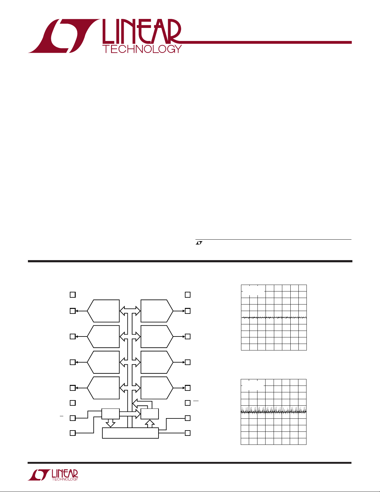
BLOCK DIAGRA
1GND
2
V
OUT A
V
3 14
OUT B
V
4 13
OUT C
V
5
OUT D
REF
6
7
CS/LD
SCK
8
DAC A DAC H
DAC B DAC G
DAC C DAC F
DAC D DAC E
CONTROL
LOGIC
W
SHIFT REGISTER
ADDRESS
DECODER
16
15
12
11
10
9
1665/60 BD
V
V
V
V
V
CLR
D
D
CC
OUT H
OUT G
OUT F
OUT E
OUT
IN
LTC1665 Differential Nonlinearity (DNL)
0.5
VCC = 5V
0.4
V
= 4.096V
REF
0.3
0.2
0.1
0
LSB
–0.1
–0.2
–0.3
–0.4
–0.5
0 64 128 192 255
CODE
1665/60 G09
LTC1660 Differential Nonlinearity (DNL)
1
VCC = 5V
0.8
V
= 4.096V
REF
0.6
0.4
0.2
0
LSB
–0.2
–0.4
–0.6
–0.8
–1
0 256 512 768 1023
CODE
1665/60 G13
1

LTC1665/LTC1660
WU
A
W
O
LUTEXI TIS
S
A
WUW
ARB
U
G
PACKAGE
/
O
RDER I FOR ATIO
(Note 1)
VCC to GND .............................................. –0.2V to 7.5V
Logic Inputs to GND ................................ –0.2V to 7.5V
V
OUT A
, V
OUT B…VOUT H
,
REF to GND ................................. –0.2V to (VCC + 0.2V)
Maximum Junction Temperature ......................... 125°C
Operating Temperature Range
LTC1665C/LTC1660C ............................ 0°C to 70°C
LTC1665I/LTC1660I .......................... –40°C to 85°C
Storage Temperature Range ................ –65°C to 150°C
Lead Temperature (Soldering, 10 sec)................ 300°C
LECTRICAL C CHARA TERIST
E
ICS
TOP VIEW
1
GND
2
V
OUT A
3
V
OUT B
4
V
OUT C
5
V
OUT D
6
REF
7
CS/LD
8
SCK
GN PACKAGE
16-LEAD PLASTIC SSOP
T
= 125°C, θJA = 150°C/W (GN)
JMAX
T
= 125°C, θJA = 100°C/W (N)
JMAX
Consult factory for Military grade parts.
V
16
CC
V
15
OUT H
V
14
OUT G
V
13
OUT F
V
12
OUT E
CLR
11
D
10
OUT
D
9
IN
N PACKAGE
16-LEAD PDIP
ORDER PART
NUMBER
LTC1665CGN
LTC1665CN
LTC1665IGN
LTC1665IN
LTC1660CGN
LTC1660CN
LTC1660IGN
LTC1660IN
GN PART MARKING
1665
1665I
1660
1660I
The ● denotes specifications which apply over the full operating temperature range, otherwise specifications
are at TA = 25°C. VCC = 2.7V to 5.5V, V
SYMBOL PARAMETER CONDITIONS MIN TYP MAX MIN TYP MAX UNITS
Accuracy
Resolution ● 8 10 Bits
Monotonicity V
DNL Differential Nonlinearity V
INL Integral Nonlinearity V
V
OS
FSE Full-Scale Error VCC = 5V, V
PSR Power Supply Rejection V
Offset Error (Note 7) ● ±10 ±30 ±10 ±30 mV
VOS Temperature Coefficient ● ±15 ±15 µV/°C
Full-Scale Error Temperature Coefficient ● ±30 ±30 µV/°C
≤ VCC, V
REF
unloaded, unless otherwise noted.
OUT
LTC1665 LTC1660
≤ VCC – 0.1V (Note 2) ● 8 10 Bits
REF
≤ VCC – 0.1V (Note 2) ● ±0.1 ±0.5 ±0.2 ±0.75 LSB
REF
≤ VCC – 0.1V (Note 2) ● ±0.2 ±1.0 ±0.6 ±2.5 LSB
REF
= 4.096V ● ±1 ±4 ±3 ±15 LSB
REF
= 2.5V 0.045 0.18 LSB/V
REF
U
The ● denotes specifications which apply over the full operating temperature range, otherwise specifications
are at TA = 25°C. VCC = 2.7V to 5.5V, V
SYMBOL PARAMETER CONDITONS MIN TYP MAX UNITS
Reference Input
Input Voltage Range ● 0V
Resistance Not in Sleep Mode ● 35 65 kΩ
Capacitance (Note 6) 15 pF
I
REF
Power Supply
V
CC
I
CC
Reference Current Sleep Mode ● 0.001 1 µA
Positive Supply Voltage For Specified Performance ● 2.7 5.5 V
Supply Current VCC = 5V (Note 3) ● 450 730 µA
≤ VCC, V
REF
unloaded, unless otherwise noted.
OUT
= 3V (Note 3) ● 340 550 µA
V
CC
Sleep Mode (Note 3)
● 13µA
CC
2
V
LTC1665/LTC1660
LECTRICAL C CHARA TERIST
E
ICS
The ● denotes specifications which apply over the full operating temperature range, otherwise specifications
are at TA = 25°C. VCC = 2.7V to 5.5V, V
SYMBOL PARAMETER CONDITIONS MIN TYP MAX UNITS
DC Performance
Short-Circuit Current Low V
Short-Circuit Current High V
AC Performance
Voltage Output Slew Rate Rising (Notes 4, 5) 0.60 V/µs
Voltage Output Settling Time To ±0.5LSB (Notes 4, 5) 30 µs
Capacitive Load Driving 1000 pF
Digital I/O
V
IH
V
IL
V
OH
V
OL
I
LK
C
IN
Digital Input High Voltage VCC = 2.7V to 5.5V ● 2.4 V
Digital Input Low Voltage VCC = 4.5V to 5.5V ● 0.8 V
Digital Output High Voltage I
Digital Output Low Voltage I
Digital Input Leakage VIN = GND to V
Digital Input Capacitance (Note 6) ● 10 pF
≤ VCC, V
REF
= 0V, VCC = 5.5V, V
OUT
= VCC = 5.5V, V
OUT
Falling (Notes 4, 5) 0.25 V/µs
= 2.7V to 3.6V ● 2.0 V
V
CC
VCC = 2.7V to 5.5V ● 0.6 V
= –1mA, D
OUT
= 1mA, D
OUT
unloaded, unless otherwise noted.
OUT
= 5.1V, Code = Full Scale ● 10 30 100 mA
REF
= 5.1V, Code = 0 ● 10 27 120 mA
REF
Only ● VCC – 1 V
OUT
Only ● 0.4 V
OUT
CC
● ±10 µA
UW
TI I G CHARACTERISTICS
range, otherwise specifications are at TA = 25°C. (See Figure 1)
SYMBOL PARAMETER CONDITIONS MIN TYP MAX UNITS
VCC = 4.5V to 5.5V
t
1
t
2
t
3
t
4
t
5
t
6
t
7
t
8
t
9
t
10
t
11
VCC = 2.7V to 5.5V
t
1
t
2
t
3
t
4
t
5
DIN Valid to SCK Setup ● 40 15 ns
DIN Valid to SCK Hold ● 0 –11 ns
SCK High Time (Note 6) ● 30 5 ns
SCK Low Time (Note 6) ● 30 7 ns
CS/LD Pulse Width (Note 6) ● 80 30 ns
LSB SCK High to CS/LD High (Note 6) ● 30 4 ns
CS/LD Low to SCK High (Note 6) ● 80 26 ns
D
Propagation Delay C
OUT
SCK Low to CS/LD Low (Note 6) ● 20 0 ns
CLR Pulse Width (Note 6) ● 100 37 ns
CS/LD High to SCK Positive Edge (Note 6) ● 30 0 ns
SCK Frequency Continuous Square Wave (Note 6) ● 5.00 MHz
DIN Valid to SCK Setup (Note 6) ● 60 20 ns
DIN Valid to SCK Hold (Note 6) ● 0 –14 ns
SCK High Time (Note 6) ● 50 8 ns
SCK Low Time (Note 6) ● 50 12 ns
CS/LD Pulse Width (Note 6) ● 100 30 ns
The ● denotes specifications which apply over the full operating temperature
= 15pF (Note 6) ● 52680ns
LOAD
Continuous 23% Duty Cycle Pulse (Note 6)
Gated Square Wave (Note 6) ● 16.7 MHz
● 7.69 MHz
3
LTC1665/LTC1660
UW
TI I G CHARACTERISTICS
range, otherwise specifications are at TA = 25°C. (See Figure 1)
SYMBOL PARAMETER CONDITIONS MIN TYP MAX UNITS
t
6
t
7
t
8
t
9
t
10
t
11
LSB SCK High to CS/LD High (Note 6) ● 50 5 ns
CS/LD Low to SCK High (Note 6) ● 100 27 ns
D
Propagation Delay C
OUT
SCK Low to CS/LD Low (Note 6) ● 30 0 ns
CLR Pulse Width (Note 6) ● 120 41 ns
CS/LD High to SCK Positive Edge (Note 6) ● 30 0 ns
SCK Frequency Continuous Square Wave (Note 6) ● 3.85 MHz
The ● denotes specifications which apply over the full operating temperature
= 15pF (Note 6) ● 5 47 150 ns
LOAD
Continuous 28% Duty Cycle Pulse ● 5.55 MHz
Gated Square Wave
● 10 MHz
Note 1: Absolute maximum ratings are those values beyond which the life
of a device may be impaired.
Note 2: Nonlinearity and monotonicity are defined from code 4 to code
255 for the LTC1665 and from code 20 to code 1023 for the LTC1660.
See Applications Information.
Note 3: Digital inputs at 0V or VCC.
Note 5: VCC = V
i.e., codes 26 and 230 for the LTC1665 or codes 102 and 922 for the
LTC1660.
Note 6: Guaranteed by design and not production tested.
Note 7: Measured at code 4 for the LTC1665 and code 20 for the
LTC1660.
Note 4: Load is 10kΩ in parallel with 100pF.
UW
TYPICAL PERFOR A CE CHARACTERISTICS
Midscale Output Voltage
vs Load Current
3
V
= V
REF
CC
CODE = 128 (LTC1665)
2.9
CODE = 512 (LTC1660)
2.8
2.7
2.6
(V)
2.5
OUT
V
2.4
2.3
2.2
2.1
2
–30 –20 –10 0 10 20 30
VCC = 5.5V
VCC = 5V
VCC = 4.5V
I
(mA)
OUT
SINKSOURCE
1665/60 G01
2
1.9
1.8
1.7
1.6
(V)
1.5
OUT
V
1.4
1.3
1.2
1.1
1
–15 – 4–8–12 0 4 8 12 15
= 5V. DAC switched between 0.1VFS and 0.9VFS,
REF
(LTC1665/LTC1660)
Midscale Output Voltage
vs Load Current
V
= V
REF
CC
CODE = 128 (LTC1665)
CODE = 512 (LTC1660)
VCC = 3.6V
VCC = 3V
VCC = 2.7V
SINKSOURCE
I
(mA)
OUT
1665/60 G02
4
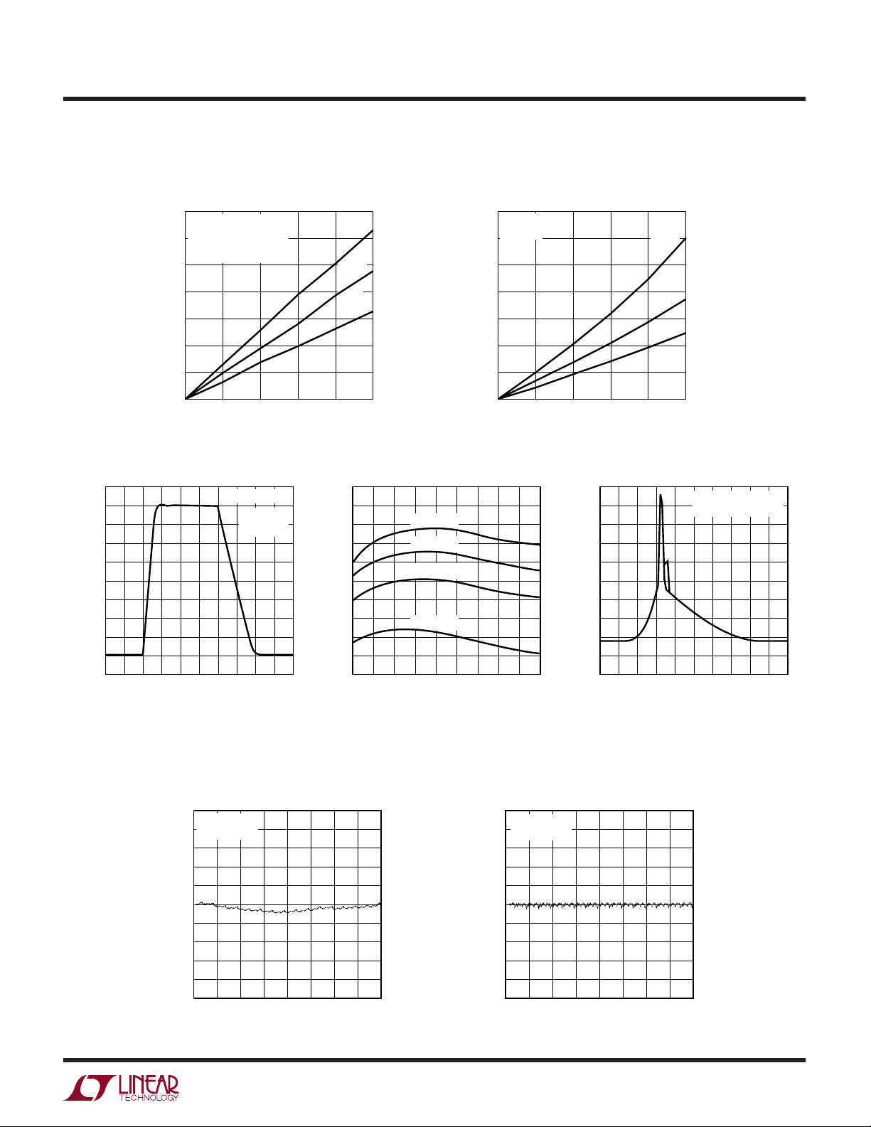
UW
LOGIC INPUT VOLTAGE (V)
012345
SUPPLY CURRENT (mA)
1665/60 G07
2
1.6
1.2
0.8
0.4
0
ALL DIGITAL INPUTS
SHORTED TOGETHER
TYPICAL PERFOR A CE CHARACTERISTICS
LTC1665/LTC1660
(LTC1665/LTC1660)
Minimum Supply Headroom vs
Load Current (Output Sourcing)
1400
V
= 4.096V
REF
< 1LSB
∆V
OUT
1200
CODE = 255 (LTC1665)
CODE = 1023 (LTC1660)
1000
(mV)
800
OUT
600
– V
CC
V
400
200
0
0246810
|
I
|
(mA) (Sourcing)
OUT
Large-Signal Step Response Supply Current vs Logic Input Voltage
5
4
3
(V)
OUT
V
2
1
0
0 20406080100
TIME (µs)
VCC= V
10% TO
90% STEP
REF
1665/60 G05
= 5V
125°C
25°C
–55°C
1665/60 G03
Supply Current vs Temperature
500
480
460
440
420
400
380
360
SUPPLY CURRENT (µA)
340
320
300
–55 –35 –15 5 25 45 65 85 105 125
VCC = 5.5V
VCC = 4.5V
VCC = 3.6V
VCC = 2.7V
TEMPERATURE (°C)
Minimum V
Load Current (Output Sinking)
1400
VCC = 5V
CODE = 0
1200
1000
800
(mV)
OUT
600
V
400
200
0
0246810
1665/60 G06
OUT
|
I
|
(mA) (Sinking)
OUT
vs
125°C
25°C
–55°C
1665/60 G04
TYPICAL PERFOR A CE CHARACTERISTICS
Integral Nonlinearity (INL)
1
0.8
0.6
0.4
0.2
0
LSB
–0.2
–0.4
–0.6
–0.8
–1
0 64 128 192 255
VCC = 5V
= 4.096V
V
REF
UW
CODE
1665/60 G08
(LTC1665)
Differential Nonlinearity (DNL)
0.5
VCC = 5V
0.4
0.3
0.2
0.1
LSB
–0.1
–0.2
–0.3
–0.4
–0.5
= 4.096V
V
REF
0
0 64 128 192 255
CODE
1665/60 G09
5
 Loading...