

Linear Technology LTC1663 Datasheet
FEATURES
LTC1663
10-Bit Rail-to-Rail
Micropower DAC with 2-Wire Interface
U
DESCRIPTIO
■
Micropower 10-Bit DAC in SOT-23
■
Low Operating Current: 60µA
■
Ultralow Power Shutdown Mode: 10µA
■
2-Wire Serial Interface Compatible
with SMBus and I2C
■
Single 2.7V to 5.5V Operation
■
Selectable Internal Reference or Ratiometric to V
■
Buffered True Rail-to-Rail Voltage Output
■
Maximum DNL Error: 0.75LSB
■
Power-On Reset
■
8 User Selectable Addresses (MSOP Package)
■
0.6V VIL and 1.4V VIH for SDA and SCL
■
Small 5-Lead SOT-23 and 8-Lead MSOP Packages
TM
U
APPLICATIO S
■
Digital Calibration
■
Offset/Gain Adjustment
■
Industrial Process Control
■
Automatic Test Equipment
■
Arbitrary Function Generators
■
Battery-Powered Data Conversion Products
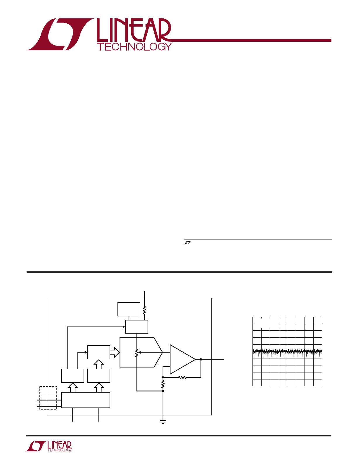
The LTC®1663 is a 10-bit voltage output DAC with true
buffered rail-to-rail output voltage capability. It operates
from a single supply with a range of 2.7V to 5.5V. The
reference for the DAC is selectable between the supply
voltage or an internal bandgap reference. Selecting the
internal bandgap reference will set the full-scale output
voltage range to 2.5V. Selecting the supply as the refer-
CC
ence sets the output voltage range to the supply voltage.
The part features a simple 2-wire serial interface compat-
ible with SMBus and I2C that allows communication
between many devices. The internal data registers are
double buffered to allow for simultaneous update of
several devices at once. The DAC can be put in low current
power-down mode for use in power conscious systems.
Power-on reset ensures the DAC output is at 0V when
power is initially applied, and all internal registers are
cleared.
, LTC and LT are registered trademarks of Linear Technology Corporation.
I2C is a trademark of Philips Electronics N.V.
BLOCK DIAGRA
DAC LATCH
AD0
AD1
AD2
COMMAND
LATCH
2-WIRE INTERFACE
SDA
1 (1) 5 (4)
MSOP
PACKAGE
ONLY
(6)
(2)
(3)
NOTE: PIN NUMBERS IN PARENTHESES REFER TO THE MSOP PACKAGE
10-BIT
INPUT
LATCH
SCL
W
1.25V
BANDGAP
REFERENCE
REFERENCE
SELECT
4 (5)
V
CC
R
GND
2 (7)
Differential Nonlinearity (DNL)
1.0
V
= VCC = 5V
REF
0.8
= 25°C
T
A
0.6
0.4
0.2
+
–
R
V
OUT
1663 BD
3 (8)
0
–0.2
ERROR (LSB)
–0.4
–0.6
–0.8
–1.0
0
28 384
156
512
CODE
640
768
896
1024
1663 G02
1
LTC1663
A
W
O
LUTEXI TIS
S
A
WUW
U
ARB
G
(Note 1)
VCC to GND .............................................. –0.3V to 7.5V
SDA, SCL ..................................................–0.3V to 7.5V
AD0, AD1, AD2 (MSOP Only) ...... – 0.3V to (VCC + 0.3V)
V
............................................ –0.3V to (VCC + 0.3V)
OUT
WU
/
PACKAGE
SDA
AD1
AD2
SCL
8-LEAD PLASTIC MSOP
T
JMAX
Consult factory for Military grade parts.
LECTRICAL C CHARA TERIST
E
temperature range, otherwise specifications are at T
unless otherwise noted.
O
RDER I FOR ATIO
TOP VIEW
1
2
3
4
MS8 PACKAGE
= 125°C, θJA = 150°C/W
ORDER PART
NUMBER
8
V
OUT
7
GND
6
AD0
5
V
CC
LTC1663CMS8
LTC1663IMS8
MS8 PART MARKING
LTEQ
LTJJ
ICS
The ● denotes specifications which apply over the full operating
= 25°C. V
A
Operating Temperature Range
LTC1663C .............................................. 0°C to 70°C
LTC1663I........................................... –40°C to 85°C
Storage Temperature Range ................ –65°C to 150°C
Lead Temperature (Soldering, 10 sec)................. 300°C
U
ORDER PART
NUMBER
LTC1663CS5
S5 PART MARKING
LTEP
unloaded,
SDA 1
GND 2
V
OUT
T
JMAX
= 2.7V to 5.5V, V
CC
TOP VIEW
3
S5 PACKAGE
5-LEAD PLASTIC SOT-23
= 125°C, θJA = 250°C/W
set as reference, V
CC
5 SCL
4 V
CC
OUT
SYMBOL PARAMETER CONDITIONS MIN TYP MAX UNITS
DAC
Resolution ● 10 Bits
Monotonicity (Note 2) ● 10 Bits
DNL Differential Nonlinearity Guaranteed Monotonic (Note 2) ● ±0.2 ±0.75 LSB
INL Integral Nonlinearity (Note 2) ● ±0.5 ±2.5 LSB
V
OS
V
OSTC
FSE Full-Scale Error Reference Set to V
V
OUT
V
FSTC
PSRR Power Supply Rejection Ratio Reference Set to Internal Bandgap, ±0.4 LSB/V
Power Supply
V
CC
I
CC
I
SD
Op Amp DC Performance
Offset Error Measured at Code 20 ● ±10 ±30 mV
Offset Error Temperature Coefficient ±15 µV/°C
Reference Set to Internal Bandgap
DAC Output Span Reference Set to V
Full-Scale Voltage Temperature Coefficient ±30 µV/°C
Positive Supply Voltage ● 2.7 5.5 V
Supply Current VCC = 3V (Note 3) ● 60 100 µA
Supply Current in Shutdown Mode (Note 3) ● 10 16 µA
Short-Circuit Current (Sourcing) V
Short-Circuit Current (Sinking) V
Output Impedance to GND Input Code = 0, VCC = 5V 65 Ω
Reference Set to Internal Bandgap 0 to 2.5 V
Code = 1023
VCC = 5V (Note 3) ● 75 125 µA
Shorted to GND, Input Code = 1023 ● 25 100 mA
OUT
Shorted to VCC, Input Code = 0 ● 30 120 mA
OUT
Input Code = 0, V
In Shutdown Mode 500 kΩ
CC
CC
= 3V 150 Ω
CC
● ±3 ±15 LSB
● ±3 ±15 LSB
0 to V
CC
V
2

LTC1663
LECTRICAL C CHARA TERIST
E
ICS
temperature range, otherwise specifications are at T
The ● denotes specifications which apply over the full operating
= 25°C. V
A
= 2.7V to 5.5V, V
CC
set as reference, V
CC
unloaded,
OUT
unless otherwise noted.
SYMBOL PARAMETER CONDITIONS MIN TYP MAX UNITS
Output Impedance to V
AC Performance
Voltage Output Slew Rate Rising (Notes 4, 5) 0.75 V/µs
Voltage Output Settling Time To ±0.5LSB (Notes 4, 5) 30 µs
Digital Feedthrough 0.75 nV • s
Digital-to-Analog Glitch Impulse 1LSB Change Around Major Carry 70 nV • s
Digital Inputs SCL, SDA
V
IH
V
IL
V
LTH
I
LEAK
C
IN
Digital Output SDA
V
OL
Address Inputs AD0, AD1, AD2 (MSOP Only)
I
UP
V
IH
V
IL
High Level Input Voltage ● 1.4 V
Low Level Input Voltage ● 0.6 V
Logic Threshold Voltage 1V
Digital Input Leakage VCC = 5.5V and 0V, VIN = GND to V
Digital Input Capacitance (Note 7) ● 10 pF
Digital Output Low Voltage I
Address Pin Pull-Up Current VIN = 0V ● 0.5 1.5 µA
High Level Input Voltage ● VCC – 0.3 V
Low Level Input Voltage ● 0.8 V
CC
Input Code = 1023, VCC = 5V 80 Ω
Input Code = 1023, V
Falling (Notes 4, 5) 0.25 V/µs
= 350µA ● 0.4 V
PULLUP
= 3V 120 Ω
CC
CC
● ±1 µA
UW
TI I G CHARACTERISTICS
range, otherwise specifications are at T
SYMBOL PARAMETER MIN TYP MAX UNITS
SMBus Timing Characteristics (Notes 6, 7)
f
SMB
t
BUF
t
HD, STA
t
SU, STA
t
SU, STO
t
HD, DAT
t
SU, DAT
t
LOW
t
HIGH
t
f
t
r
Note 1: Absolute maximum ratings are those values beyond which the life
of a device may be impaired.
Note 2: Nonlinearity and monotonicity are defined from code 20 to code
1003 (full scale). See Applications Information.
Note 3: Digital inputs at 0V or V
SMBus Operating Frequency ● 10 100 kHz
Bus Free Time Between Stop and Start Condition ● 4.7 µs
Hold Time After (Repeated) Start Condition ● 4.0 µs
Repeated Start Condition Setup Time ● 4.7 µs
Stop Condition Setup Time ● 4.0 µs
Data Hold Time ● 300 ns
Data Setup Time ● 250 ns
Clock Low Period ● 4.7 µs
Clock High Period ● 4.0 50 µs
Clock, Data Fall Time ● 300 ns
Clock, Data Rise Time ● 1000 ns
.
CC
= 25°C. V
A
The ● denotes specifications which apply over the full operating temperature
= 2.7V to 5.5V, V
CC
set as reference, V
CC
Note 4: Load is 10kΩ in parallel with 100pF.
= V
Note 5: V
i.e., codes k = 102 and k = 922.
Note 6: All values are referenced to V
Note 7: Guaranteed by design and not subject to test.
CC
= 5V. DAC switched between 0.1VFS and 0.9VFS,
REF
unloaded, unless otherwise noted.
OUT
and VIL levels.
IH
3
LTC1663
UW
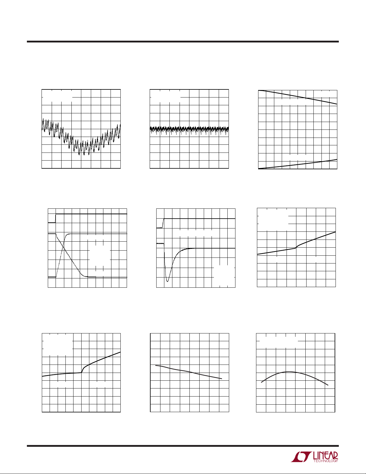
TYPICAL PERFOR A CE CHARACTERISTICS
1.0
V
REF
0.8
T
A
0.6
0.4
0.2
0
–0.2
ERROR (LSB)
–0.4
–0.6
–0.8
–1.0
0
= VCC = 5V
= 25°C
28 384
156
512
CODE
640
768
896
1024
1663 G01
1.0
V
REF
0.8
T
A
0.6
0.4
0.2
0
–0.2
ERROR (LSB)
–0.4
–0.6
–0.8
–1.0
0
= VCC = 5V
= 25°C
28 384
156
512
CODE
640
768
896
1663 G02
1024
Source and Sink Current
Capability with VCC = 5VDifferential Nonlinearity (DNL)Integral Nonlinearity (INL)
5.0
4.5
4.0
3.5
3.0
2.5
2.0
1.5
OUTPUT VOLTAGE (V)
1.0
0.5
0
01 3
DAC CODE = 1023
DAC CODE = 0
2
46579
OUTPUT CURRENT SOURCE/SINK (mA)
TA = 25°C
8
1011 G03
10
Large-Signal Step Response Midscale Glitch
5
SDA
(VOLTS)
0
V
OUT
(VOLTS)
5
4
3
2
1
0
CODE = 990
VCC = 5V
R
C
T
5µs/DIV
CODE = 32
Load Regulation vs Output Current
1.0
0.8
0.6
0.4
0.2
(LSB)
OUT
–0.2
∆V
–0.4
–0.6
–0.8
–1.0
VCC = V
V
CODE = 512
T
0
–1.0
= 3V
REF
= 1.5V
OUT
= 25°C
A
SOURCE SINK
–0.8 – 0.2
–0.6–0.4
I
OUT
0
(mA)
0.2
= 4.7k
L
= 100pF
L
= 25°C
A
Load Regulation vs Output Current
1.0
VCC = V
0.8
5V
SDA
1663 G04
V
OUT
10mV/DIV
0V
CODE = 512 TO 511
2µs/DIV
VCC = 5V
R
= 4.7k
L
= 100pF
C
L
= 25°C
T
A
1663 G05
Offset Error Voltage vs
Temperature
5
4
3
2
1
0
–1
–2
–3
OFFSET ERROR VOLTAGE (mV)
–4
0.8
1.0
0.60.4
1663 G07
–5
–60
–20
–40 0
TEMPERATURE (°C)
20
40
80
60
100
1663 G08
V
CODE = 512
0.6
T
0.4
0.2
(LSB)
0
OUT
–0.2
∆V
–0.4
–0.6
–0.8
–1.0
–4
Full-Scale Output Voltage vs
Temperature
2.510
2.508
2.506
2.504
2.502
2.500
2.498
2.496
OUTPUT VOLTAGE (V)
2.494
2.492
2.490
–60
= 5V
REF
= 2.5V
OUT
= 25°C
A
SOURCE SINK
–3 –1
–2
REFERENCE SET TO
INTERNAL BANDGAP
–20
–40 0
0
I
(mA)
OUT
20
TEMPERATURE (°C)
3
2
1
60
40
80
4
1663 G06
100
1663 G09
4
 Loading...