

Linear Technology LTC1661 Datasheet
FEATURES
LTC1661
Micropower Dual
10-Bit DAC in MSOP
U
DESCRIPTIO
■
Tiny: Two 10-Bit DACs in an 8-Lead MSOP—
Half the Board Space of an SO-8
■
Micropower: 60µA per DAC
Sleep Mode: 1µA for Extended Battery Life
■
Rail-to-Rail Voltage Outputs Drive 1000pF
■
Wide 2.7V to 5.5V Supply Range
■
Double Buffered for Independent or Simultaneous
DAC Updates
■
Reference Range Includes Supply for Ratiometric
0V-to-VCC Output
■
Reference Input Has Constant Impedance over All
Codes (260kΩ Typ)—Eliminates External Buffers
■
3-Wire Serial Interface with
Schmitt Trigger Inputs
■
Differential Nonlinearity: ≤±0.75LSB Max
U
APPLICATIO S
■
Mobile Communications
■
Digitally Controlled Amplifiers and Attenuators
■
Portable Battery-Powered Instruments
■
Automatic Calibration for Manufacturing
■
Remote Industrial Devices
, LTC and LT are registered trademarks of Linear Technology Corporation.
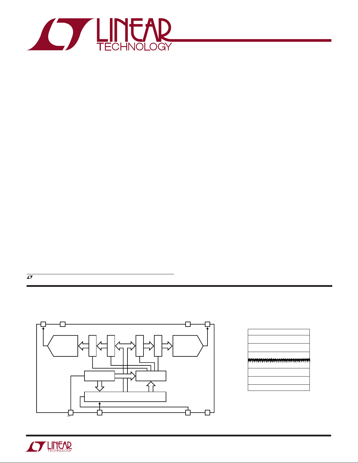
The LTC®1661 integrates two accurate, serially addressable, 10-bit digital-to-analog converters (DACs) in a
single tiny MS8 package. Each buffered DAC draws just
60µA total supply current, yet is capable of supplying DC
output currents in excess of 5mA and reliably driving
capacitive loads up to 1000pF. Sleep mode further reduces total supply current to a negligible 1µA.
Linear Technology’s proprietary, inherently monotonic
voltage interpolation architecture provides excellent linearity while allowing for an exceptionally small external
form factor. The double-buffered input logic provides
simultaneous update capability and can be used to write to
either DAC without interrupting Sleep mode.
Ultralow supply current, power-saving Sleep mode and
extremely compact size make the LTC1661 ideal for
battery-powered applications, while its straightforward
usability, high performance and wide supply range make
it an excellent choice as a general purpose converter.
For additional outputs and even greater board density,
please refer to the LTC1660 micropower octal DAC for
10-bit applications. For 8-bit applications, please consult
the LTC1665 micropower octal DAC.
W
BLOCK DIAGRA
V
OUT A
GND
8 5
7
10-BIT
DAC A
1 4
CS/LD
LATCH
CONTROL
LOGIC
2
SCK
LATCH
SHIFT REGISTER
LATCH
ADDRESS
DECODER
LATCH
V
10-BIT
DAC B
D
V
CC
6
3
OUT B
REF
IN
1661 BD
Differential Nonlinearity (DNL)
0.75
0.60
0.40
0.20
0
LSB
–0.20
–0.40
–0.60
–0.75
0 256 512 768 1023
CODE
1661 G02
1
LTC1661
1
2
3
4
8
7
6
5
TOP VIEW
CS/LD
SCK
D
IN
REF
V
OUT A
GND
V
CC
V
OUT B
N8 PACKAGE
8-LEAD PLASTIC DIP
A
W
O
LUTEXI TIS
S
A
WUW
U
ARB
G
(Note 1)
VCC to GND.............................................. –0.3V to 7.5V
Logic Inputs to GND ................................ –0.3V to 7.5V
V
OUT A
, V
, REF to GND............–0.3V to VCC + 0.3V
OUT B
Maximum Junction Temperature......................... 125°C
Storage Temperature Range................ –65°C to 150°C
WU
/
PACKAGE
CS/LD
SCK
D
IN
REF
8-LEAD PLASTIC MSOP
T
JMAX
Consult factory for Military grade parts.
O
RDER I FOR ATIO
TOP VIEW
1
2
3
4
MS8 PACKAGE
= 125°C, θJA = 150°C/W
ORDER PART
NUMBER
8
V
OUT A
7
GND
6
V
CC
V
5
OUT B
LTC1661CMS8
LTC1661IMS8
MS8 PART MARKING
LTDV
LTDW
Operating Temperature Range
LTC1661C ............................................. 0°C to 70°C
LTC1661I........................................... –40°C to 85°C
Lead Temperature (Soldering, 10 sec)................ 300°C
U
ORDER PART
NUMBER
LTC1661CN8
LTC1661IN8
T
= 125°C, θJA = 100°C/W
JMAX
LECTRICAL C CHARA TERIST
E
ICS
temperature range, otherwise specifications are at TA = 25°C. VCC = 2.7V to 5.5V, V
SYMBOL PARAMETER CONDITIONS MIN TYP MAX UNITS
Accuracy
Resolution ● 10 Bits
Monotonicity 1V ≤ V
DNL Differential Nonlinearity 1V ≤ V
INL Integral Nonlinearity 1V ≤ V
V
OS
FSE Full-Scale Error VCC = 5V, V
PSR Power Supply Rejection V
Reference Input
I
REF
Power Supply
V
CC
I
CC
2
Offset Error Measured at Code 20 ● ±5 ±30 mV
VOS Temperature Coefficient ±15 µV/°C
Full-Scale Error Temperature Coefficient ±30 µV/°C
Input Voltage Range ● 0V
Resistance Active Mode ● 140 260 kΩ
Capacitance ● 15 pF
Reference Current Sleep Mode ● 0.001 1 µA
Positive Supply Voltage For Specified Performance ● 2.7 5.5 V
Supply Current VCC = 5V (Note 3) ● 120 195 µA
The ● denotes the specifications which apply over the full operating
≤ VCC, V
REF
≤ VCC – 0.1V (Note 2) ● 10 Bits
REF
≤ VCC – 0.1V (Note 2) ● ±0.1 ±0.75 LSB
REF
≤ VCC – 0.1V (Note 2) ● ±0.4 ±2 LSB
REF
= 4.096V ● ±1 ±12 LSB
REF
= 2.5V 0.18 LSB/V
REF
= 3V (Note 3) ● 95 154 µA
V
CC
Sleep Mode (Note 3)
Unloaded unless otherwise noted.
OUT
CC
● 13µA
V
LTC1661
LECTRICAL C CHARA TERIST
E
ICS
temperature range, otherwise specifications are at TA = 25°C. VCC = 2.7V to 5.5V, V
SYMBOL PARAMETER CONDITIONS MIN TYP MAX UNITS
DC Performance
Short-Circuit Current Low V
Short-Circuit Current High V
AC Performance
Voltage Output Slew Rate Rising (Notes 4, 5) 0.60 V/µs
Voltage Output Settling Time To ±0.5LSB (Notes 4, 5) 30 µs
Capacitive Load Driving 1000 pF
Digital I/O
V
IH
V
IL
I
LK
C
IN
Digital Input High Voltage VCC = 2.7V to 5.5V ● 2.4 V
Digital Input Low Voltage VCC = 4.5V to 5.5V ● 0.8 V
Digital Input Leakage VIN = GND to V
Digital Input Capacitance (Note 6) ● 10 pF
The ● denotes the specifications which apply over the full operating
≤ VCC, V
REF
= 0V, VCC = V
OUT
= VCC = V
OUT
Falling (Notes 4, 5) 0.25 V/µs
= 2.7V to 3.6V ● 2.0 V
V
CC
= 2.7V to 5.5V ● 0.6 V
V
CC
= 5V, Code = 1023 ● 10 25 100 mA
REF
= 5V, Code = 0 ● 7 19 120 mA
REF
CC
Unloaded unless otherwise noted.
OUT
● ±10 µA
UW
TI I G CHARACTERISTICS
range, otherwise specifications are at TA = 25°C.
SYMBOL PARAMETER CONDITIONS MIN TYP MAX UNITS
VCC = 4.5V to 5.5V
t
1
t
2
t
3
t
4
t
5
t
6
t
7
t
9
t
11
VCC = 2.7V to 5.5V
t
1
t
2
t
3
t
4
t
5
t
6
t
7
t
9
t
11
DIN Valid to SCK Setup ● 40 15 ns
DIN Valid to SCK Hold ● 0–10 ns
SCK High Time (Note 6) ● 30 14 ns
SCK Low Time (Note 6) ● 30 14 ns
CS/LD Pulse Width (Note 6) ● 80 27 ns
LSB SCK High to CS/LD High (Note 6) ● 30 2 ns
CS/LD Low to SCK High (Note 6) ● 20 –21 ns
SCK Low to CS/LD Low (Note 6) ● 0–5 ns
CS/LD High to SCK Positive Edge (Note 6) ● 20 0 ns
SCK Frequency Square Wave (Note 6) ● 16.7 MHz
DIN Valid to SCK Setup (Note 6) ● 60 20 ns
DIN Valid to SCK Hold (Note 6) ● 0–10 ns
SCK High Time (Note 6) ● 50 15 ns
SCK Low Time (Note 6) ● 50 15 ns
CS/LD Pulse Width (Note 6) ● 100 30 ns
LSB SCK High to CS/LD High (Note 6) ● 50 3 ns
CS/LD Low to SCK High (Note 6) ● 30 –14 ns
SCK Low to CS/LD Low (Note 6) ● 0–5 ns
CS/LD High to SCK Positive Edge (Note 6) ● 30 0 ns
SCK Frequency Square Wave (Note 6) ● 10 MHz
The ● denotes the specifications which apply over the full operating temperature
Note 1: Absolute maximum ratings are those values beyond which the life
of a device may be impaired.
Note 2: Nonlinearity and monotonicity are defined from code 20 to code
1023 (full scale). See Applications Information.
3
LTC1661
UW
TI I G CHARACTERISTICS
Note 3: Digital inputs at 0V or VCC.
Note 4: Load is 10kΩ in parallel with 100pF.
Note 5: VCC = V
i.e., codes k = 102 and k = 922.
Note 6: Guaranteed by design and not subject to test.
UW
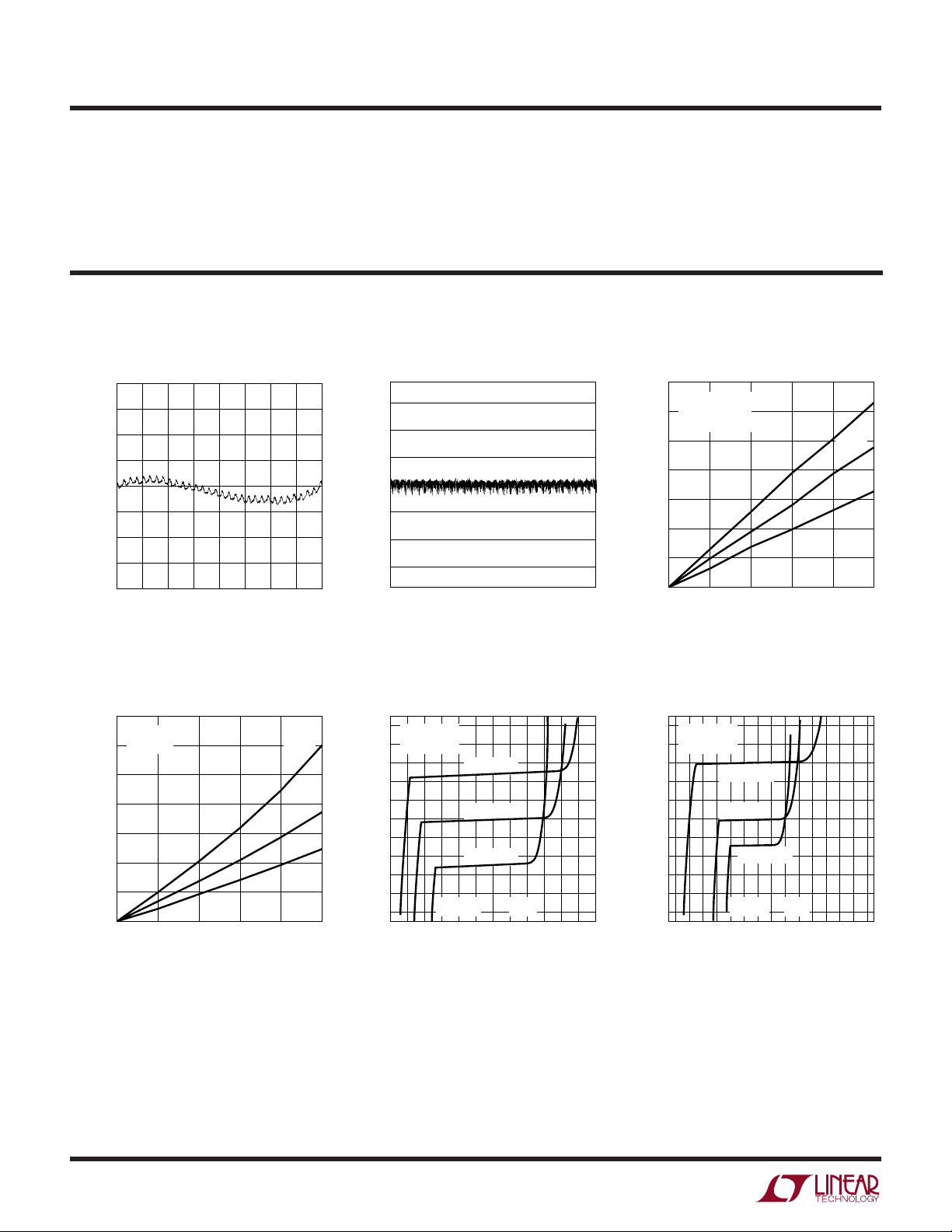
TYPICAL PERFOR A CE CHARACTERISTICS
Integral Nonlinearity (INL) Differential Nonlinearity (DNL)
2.0
1.5
1.0
0.5
0
LSB
–0.5
–1.0
–1.5
–2.0
0 256 512 768 1023
CODE
1661 G01
0.75
0.60
0.40
0.20
0
LSB
–0.20
–0.40
–0.60
–0.75
0 256 512 768 1023
CODE
= 5V. DAC switched between 0.1VFS and 0.9VFS,
REF
Minimum Supply Headroom vs
Load Current (Output Sourcing)
1400
V
= 4.096V
REF
1661 G02
1200
1000
(mV)
OUT
– V
CC
V
800
600
400
200
0
< 1LSB
∆V
OUT
CODE = 1023
0246810
|
I
|
(mA) (Sourcing)
OUT
125°C
25°C
–55°C
1661 G03
Minimum V
OUT
vs
Load Current (Output Sinking)
1400
VCC = 5V
1200
CODE = 0
1000
800
(mV)
OUT
600
V
400
200
0
0246810
|
I
|
(mA) (Sinking)
OUT
125°C
25°C
–55°C
1661 G04
Midscale Output Voltage vs
Load Current
3
V
= V
REF
2.9
2.8
2.7
2.6
(V)
2.5
OUT
V
2.4
2.3
2.2
2.1
2
–30 –20 –10 0 10 20 30
CC
CODE = 512
VCC = 5.5V
VCC = 5V
VCC = 4.5V
I
(mA)
OUT
SINKSOURCE
1661 G05
Midscale Output Voltage vs
Load Current
2
V
= V
REF
1.9
1.8
1.7
1.6
(V)
1.5
OUT
V
1.4
1.3
1.2
1.1
1
–15 –4–8–12 0 4 8 12 15
CC
CODE = 512
VCC = 3.6V
VCC = 3V
VCC = 2.7V
I
OUT
SINKSOURCE
(mA)
1661 G06
4
 Loading...