

Linear Technology LTC1657L Datasheet
LTC1657L
CODE
0
–1.0
–0.2
–0.4
–0.6
–0.8
0
0.2
0.4
0.6
0.8
1.0
DNL ERROR (LSB)
16484 32768
1657 TA02
49152
65535
Final Electrical Specifications
Parallel 16-Bit Rail-to-Rail
Micropower DAC
FEATURES
■
16-Bit Monotonic Over Temperature
■
3V Single Supply Operation
■
Deglitched Rail-to-Rail Voltage Output: 8nV • s
■
ICC: 650µA Typ
■
Maximum DNL Error: ±1LSB
■
Settling Time: 20µs to ±1LSB
■
Internal or External Reference
■
Internal Power-On Reset to 0V
■
Asynchronous CLR Pin
■
Output Buffer Configurable for Gain of 1 or 2
■
Parallel 16-Bit or 2-Byte Double Buffered Interface
■
Narrow 28-Lead SSOP Package
■
5V Version Available (LTC1657)
U
APPLICATIONS
■
Instrumentation
■
Industrial Process Control
■
Automatic Test Equipment
■
Communication Test Equipment
U
April 2000
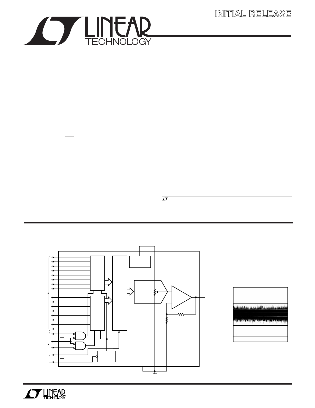
DESCRIPTION
The LTC®1657L is a complete single supply, rail-to-rail
voltage output, 16-bit digital-to-analog converter (DAC) in
a 28-pin SSOP or PDIP package. It includes a rail-to-rail
output buffer amplifier, an internal 1.25V reference and a
double buffered parallel digital interface.
The LTC1657L operates from a 2.7V to 5.5V supply. It has
a separate reference input pin that can be driven by an
external reference. The full-scale output can be 1 or 2
times the reference voltage depending on how the X1/X2
pin is connected.
The LTC1657L is similar to Linear Technology Corporation’s
LTC1450 12-bit V
grade path. It is the only buffered 16-bit parallel DAC in a
28-lead SSOP package and includes an onboard reference
for stand alone performance.
, LTC and LT are registered trademarks of Linear Technology Corporation.
DAC family allowing an easy up-
OUT
BLOCK DIAGRA
D15 (MSB)
19
18
17
16
15
14
13
FROM
12
11
10
28
27
9
8
7
6
5
4
3
1
2
D8
D7
D0 (LSB)
CSMSB
WR
CSLSB
LDAC
CLR
DATA IN FROM
MICROPROCESSOR
DATA BUS
MICROPROCESSOR
DECODE LOGIC
SYSTEM RESET
FROM
W
22 2423
REFHIREFOUT
REFERENCE
MSB
8-BIT
INPUT
REGISTER
16-BIT
DAC
REGISTER
LSB
8-BIT
INPUT
REGISTER
POWER-ON
RESET
Information furnished by Linear Technology Corporation is believed to be accurate and reliable.
However, no responsibility is assumed for its use. Linear Technology Corporation makes no representation that the interconnection of its circuits as described herein will not infringe on existing patent rights.
1.25V
16-BIT
DAC
REFLOGND
2120 26
2.7V TO 5.5V
+
–
R
X1/X2
V
CC
V
OUT
25
0V TO
2.5V
R
1657 TA01
Differential Nonlinearity
vs Input Code
1
LTC1657L
WW
W
U
ABSOLUTE MAXIMUM RATINGS
(Note 1)
VCC to GND .............................................. –0.5V to 7.5V
TTL Input Voltage,
REFHI, REFLO, X1/X2 .......................... –0.5V to 7.5V
V
, REFOUT ............................ –0.5V to (VCC + 0.5V)
OUT
Operating Temperature Range
LTC1657LC ............................................. 0°C to 70°C
LTC1657LI......................................... – 40°C to 85°C
Maximum Junction Temperature ..........................125°C
Storage Temperature Range ................ –65°C to 150°C
Lead Temperature (Soldering, 10 sec)................. 300°C
U
W
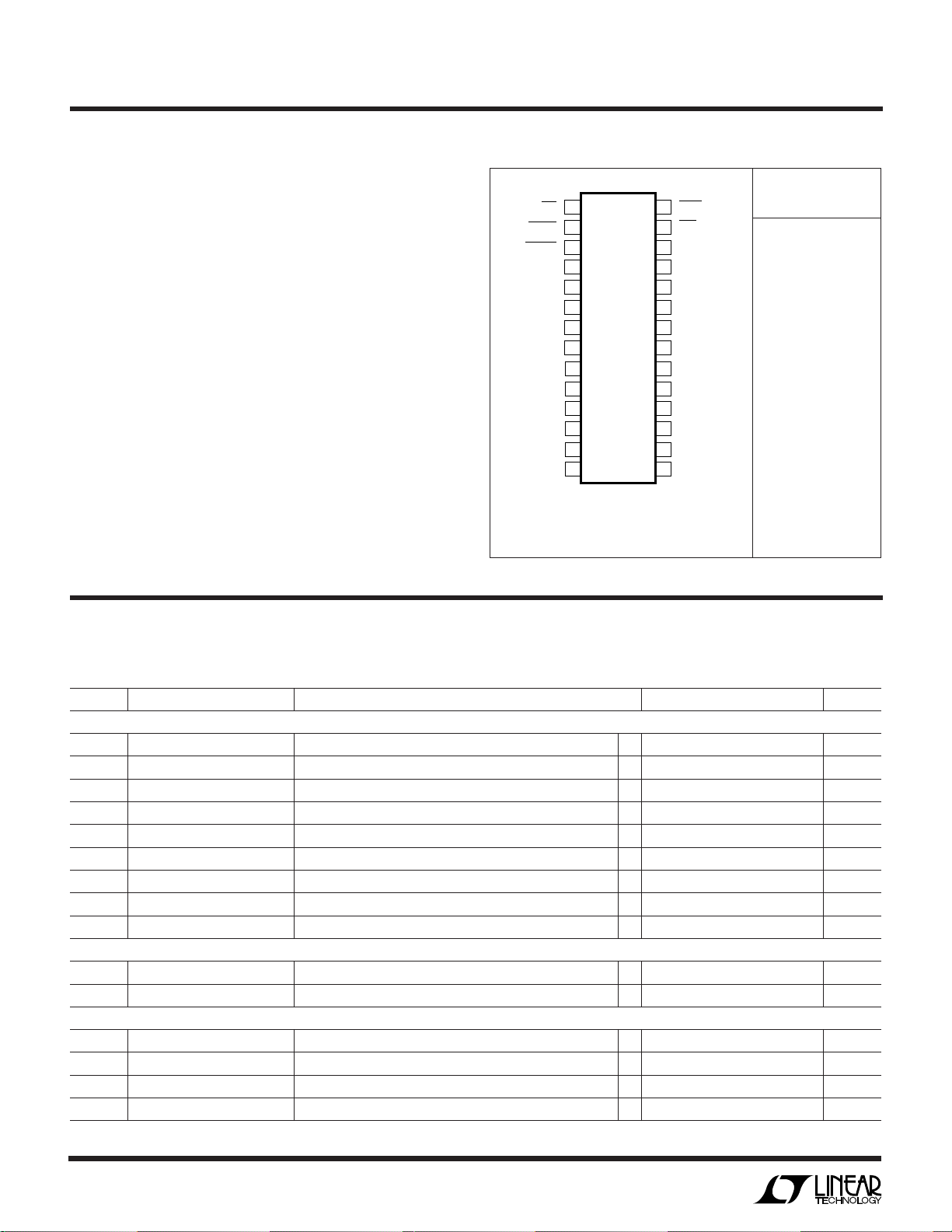
PACKAGE/ORDER INFORMATION
TOP VIEW
1
WR
2
CSLSB
3
CSMSB
(LSB) D0
Consult factory for Military grade parts.
4
5
D1
6
D2
7
D3
8
D4
9
D5
10
D6
11
D7
12
D8
13
D9
14
D10
N PACKAGE
28-LEAD PDIP
T
= 125°C, θJA = 95°C/ W (G)
JMAX
T
= 125°C, θJA = 58°C/ W (N)
JMAX
28-LEAD PLASTIC SSOP
LDAC
28
CLR
27
X1/X2
26
V
25
OUT
V
24
CC
REFOUT
23
REFHI
22
REFLO
21
GND
20
D15 (MSB)
19
D14
18
D13
17
D12
16
D11
15
GN PACKAGE
ORDER PART
NUMBER
LTC1657LCGN
LTC1657LCN
LTC1657LIGN
LTC1657LIN
U
ELECTRICAL CHARACTERISTICS
temperature range, otherwise specifications are at TA = 25°C. VCC = 2.7V to 5.5V, V
The ● denotes specifications which apply over the full operating
unloaded, REFOUT tied to REFHI,
OUT
REFLO tied to GND, X1/X2 tied to GND, unless otherwise noted.
SYMBOL PARAMETER CONDITIONS MIN TYP MAX UNITS
DAC (Note 2)
Resolution ● 16 Bits
Monotonicity ● 16 Bits
DNL Differential Nonlinearity Guaranteed Monotonic (Note 3) ● ±0.5 ±1.0 LSB
INL Integral Nonlinearity (Note 3) ● ±4 ±12 LSB
ZSE Zero Scale Error ● 02mV
V
OS
VOSTC Offset Error Tempco ±5 µV/°C
Power Supply
V
CC
I
CC
Op Amp DC Performance
Offset Error Measured at Code 200 ● ±0.3 ±4mV
Gain Error ● ±2 ±16 LSB
Gain Error Drift 1 ppm/°C
Positive Supply Voltage For Specified Performance ● 2.7 5.5 V
Supply Current 2.7V ≤ VCC ≤ 5.5V (Note 4) ● 650 1200 µA
Short-Circuit Current Low V
Short-Circuit Current High V
Output Impedance to GND Input Code = 0 ● 120 275 Ω
Output Line Regulation Input Code = 65535, VCC = 2.7V to 5.5V ● 3 mV/V
Shorted to GND ● 60 120 mA
OUT
Shorted to V
OUT
CC
● 70 140 mA
2
LTC1657L
ELECTRICAL CHARACTERISTICS
temperature range, otherwise specifications are at TA = 25°C. VCC = 2.7V to 5.5V, V
The ● denotes specifications which apply over the full operating
unloaded, REFOUT tied to REFHI,
OUT
REFLO tied to GND, X1/X2 tied to GND, unless otherwise noted.
SYMBOL PARAMETER CONDITIONS MIN TYP MAX UNITS
AC Performance
Voltage Output Slew Rate (Note 5) ● ±0.3 ±0.7 V/µs
Voltage Output Settling Time (Note 5) to 0.0015% (16-Bit Settling Time) 20 µs
(Note 5) to 0.012% (13-Bit Settling Time) 10 µs
Digital Feedthrough 0.3 nV•s
Midscale Glitch Impulse DAC Switch Between 8000H and 7FFF
Output Voltage Noise At 1kHz 200 nV/√Hz
Spectral Density
Digital I/O (VCC = 3V)
V
IH
V
IL
I
LEAK
C
IN
Switching Characteristics (VCC = 3V)
t
CS
t
WR
t
CWS
t
CWH
t
DWS
t
DWH
t
LDAC
t
CLR
Reference Output (REFOUT)
Reference Input
Digital Input High Voltage ● 2.0 V
Digital Input Low Voltage ● 0.6 V
Digital Input Leakage VIN = GND to V
Digital Input Capacitance (Note 6) 10 pF
CS (MSB or LSB) Pulse Width ● 60 ns
WR Pulse Width ● 60 ns
CS to WR Setup ● 0ns
CS to WR Hold ● 0ns
Data Valid to WR Setup ● 60 ns
Data Valid to WR Hold ● 0ns
LDAC Pulse Width ● 60 ns
CLR Pulse Width ● 60 ns
Reference Output Voltage ● 1.24 1.25 1.26 V
Reference Output 15 ppm/°C
Temperature Coefficient
Reference Line Regulation VCC = 2.7V to 5.5V ● ±1 mV/V
Reference Load Regulation Measured at I
Short-Circuit Current REFOUT Shorted to GND ● 50 100 mA
REFHI, REFLO Input Range (Note 6) See Applications Information
REFHI Input Resistance ● 16 23 kΩ
CC
= 100µA ● 3 mV/A
OUT
X1/X2 Tied to V
X1/X2 Tied to GND
OUT
H
● ±10 µA
● 0V
● 0V
8 nV•s
– 1.5 V
CC
/2
CC
Note 1: Absolute Maximum Ratings are those values beyond which the life
of a device may be impaired.
Note 2: External reference REFHI = 1.3V, V
Note 3: Nonlinearity is defined from code 128 to code 65535 (full scale).
See Applications Information.
CC
= 3V
Note 4: Digital inputs at 0V or V
Note 5: DAC switched between all 1s all 0s, slew rate is measured from
0.8V to 2V. V
Note 6: Guaranteed by design. Not subject to test.
CC
=3V.
CC
.
3
LTC1657L
UUU
PIN FUNCTIONS
WR (Pin 1): Write Input (Active Low). Used with CSMSB
and/or CSLSB to control the input registers. While WR and
CSMSB and/or CSLSB are held low, data writes into the
input register.
CSLSB (Pin 2): Chip Select Least Significant Byte (Active
Low). Used with WR to control the LSB 8-bit input registers. While WR and CSLSB are held low, the LSB byte
writes into the LSB input register. Can be connected to
CSMSB for simultaneous loading of both sets of input
latches on a 16-bit bus.
CSMSB (Pin 3): Chip Select Most Significant Byte (Active
Low). Used with WR to control the MSB 8-bit input
registers. While WR and CSMSB are held low, the MSB
byte writes into the MSB input register. Can be connected
to CSLSB for simultaneous loading of both sets of input
latches on a 16-bit bus.
D0 to D7 (Pins 4 to 11): Input data for the Least Significant
Byte. Written into LSB input register when WR = 0 and
CSLSB = 0.
D8 to D15 (Pins 12 to 19): Input data for the Most Significant Byte. Written into MSB input register when WR = 0
and CSMSB = 0.
GND (Pin 20): Ground.
REFLO (Pin 21): Lower input terminal of the DAC’s inter-
nal resistor ladder. Typically connected to Analog Ground.
An input code of (0000)H will connect the positive input of
the output buffer to this end of the ladder. Can be used to
offset the zero scale above ground.
REFHI (Pin 22): Upper input terminal of the DAC’s internal
resistor ladder. Typically connected to REFOUT. An input
code of (FFFF)H will connect the positive input of the
output buffer to 1LSB below this voltage.
REFOUT (Pin 23): Output of the internal 1.25V reference.
Typically connected to REFHI to drive internal DAC resistor
ladder.
VCC (Pin 24): Positive Power Supply Input. 2.7V ≤ VCC ≤
5.5V. Requires a 0.1µF bypass capacitor to ground.
V
(Pin 25): Buffered DAC Output.
OUT
X1/X2 (Pin 26): Gain Setting Resistor Pin. Connect to GND
for G = 2 or to V
tied to a low impedance source, such as ground or V
to ensure stability of the output buffer when driving
capacitive loads.
CLR (Pin 27): Clear Input (Asynchronous Active Low). A
low on this pin asynchronously resets all input and DAC
registers to 0s.
LDAC (Pin 28): Load DAC (Asynchronous Active Low).
Used to asynchronously transfer the contents of the input
registers to the DAC register which updates the output
voltage. If held low, the DAC register loads data from the
input registers which will immediately update V
for G = 1. This pin should always be
OUT
OUT
.
OUT
,
4
 Loading...